

ICS511
p
LOCO™ PLL Clock Multiplier
Description
The ICS511 LOCO™ is the most cost effective
way to generate a high quality, high frequency
clock output from a lower frequency crystal or
clock input. The name LOCO stands for LOw
Cost Oscillator, as it is designed to replace crystal
oscillators in most electronic systems. Using PhaseLocked-Loop (PLL) techniques, the device uses a
standard fundamental mode, inexpensive crystal
to produce output clocks up to 200 MHz.
Stored in the chip’s ROM is the ability to generate
nine different popular multiplication factors,
allowing one chip to output many common
frequencies (see page 2).
The device also has an Output Enable pin that tristates the clock output when the OE pin is taken
low.
Features
• Packaged as 8 pin SOIC or die
• Upgrade of popular ICS501 with:
- changed multiplier table
- faster operating frequencies
- output duty cycle at VDD/2
• Zero ppm multiplication error
• Input crystal frequency of 5 - 27 MHz
• Input clock frequency of 2 - 50 MHz
• Output clock frequencies up to 200 MHz
• Extremely low jitter - 25 ps one sigma
• Compatible with all popular CPUs
• Duty cycle of 45/55 up to 200 MHz
• Mask option for 9 selectable frequencies
• Operating voltages of 3.0 to 5.5V
• Tri-state output for board level testing
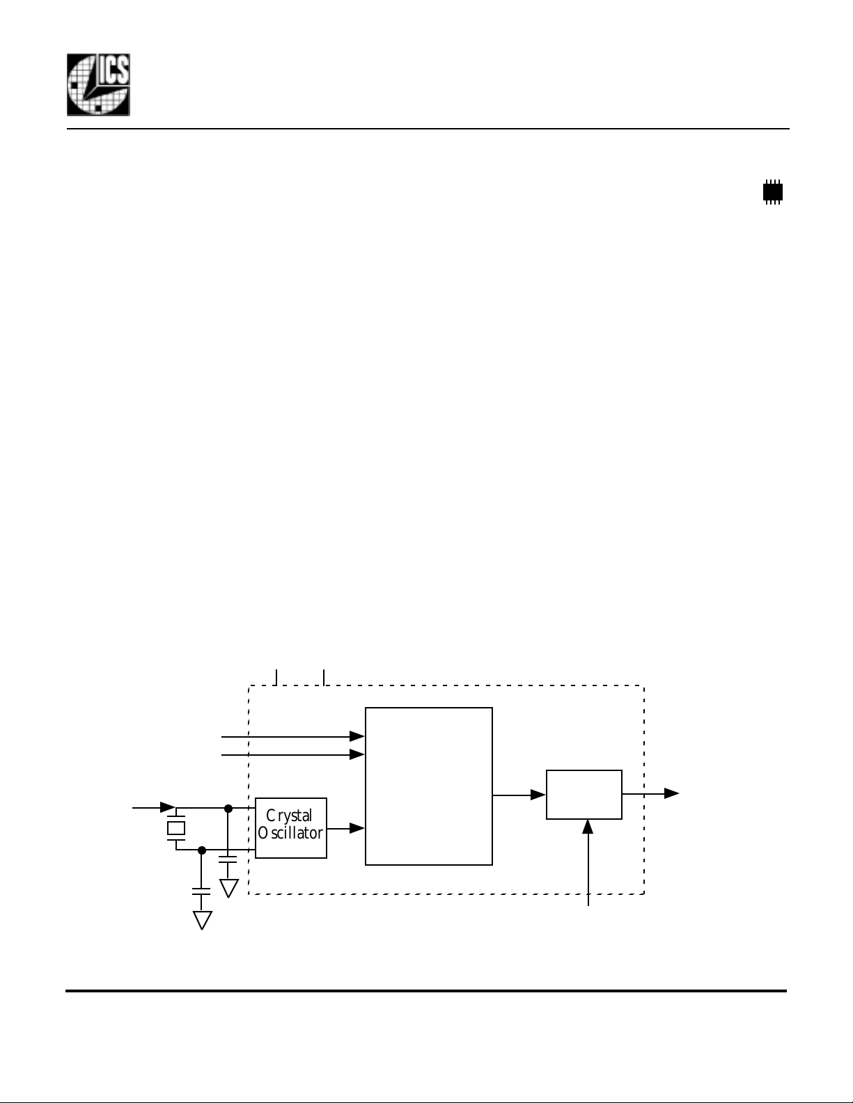
Block Diagram
Crystal or
clock in
ut
X1/ICLK
X2
VDD GND
S0
S1
Crystal
Oscillator
Optional crystal capacitors
• Industrial temperature version available
• Advanced, low power CMOS process
PLL
Clock Multiplier
Circuitry
and
ROM
Output
Buffer
Output Enable
CLK
MDS 511 C 1 Revision 061300 Printed 12/4/00
Integrated Circuit Systems, Inc. • 525 Race Street • San Jose •CA•95126•(408) 295-9800tel • www.icst.com
ICS511
g
p
LOCO™ PLL Clock Multiplier
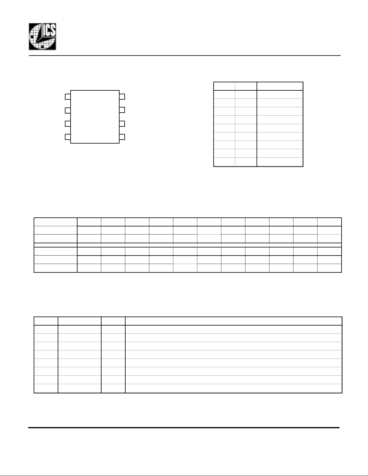
Pin Assignment
X1/ICLK
VDD
GND
S1
18
2
3
4
X2
7
OE
6
S0
5
CLK
Clock Output Table
S1 S0 CLK
0 0 4X input
0 M 5.333X input
0 1 5X input
M 0 2.5X input
M M 2X input
M 1 3.333X input
1 0 6X input
1 M 3X input
1 1 8X input
0 = connect directly to ground.
1 = connect directly to VDD.
M = leave unconnected (floatin
).
Common Output Frequencies Examples (MHz)
Output 20 24 30 32 33.33 37.5 40 48 50 60 64
Input 10 12 10 16 16.66 15 10 12 20 10 16
Selection (S1, S0) M, M M, M 1, M M, M M, M M, 0 0, 0 0, 0 M, 0 1, 0 0, 0
Output 66.66 72 75 80 83.33 90 100 120 125 133.33 150
Input 20 12 25 10 25 15 20 15 25 25 25
Selection (S1, S0) M, 1 1, 0 1, M 1, 1 M, 1 1, 0 0, 1 1, 1 0, 1 0, M 1, 0
Note that all of the above outputs are achieved by using a common, inexpensive 10MHz to 25MHz crystal.
Consult ICS on how to achieve other out
ut frequencies.
Pin Descriptions
Number Name Type Description
1 X1/ICLK XI Crystal connection or clock input.
2 VDD P Connect to +3.3V or +5V.
3 GND P Connect to ground.
4 S1 TI Multiplier select pin 1. Connect to GND or VDD or float (no connection).
5 CLK O Clock output per Table above.
6 S0 TI Multiplier select pin 0. Connect to GND or VDD or float (no connection).
7 OE I Output Enable. Tri-states CLK output when low. Internal pull-up.
8 X2 X O Crystal connection. Leave unconnected for clock input.
Key: XI/XO = Crystal Connections, I = Input, TI = Tri-Level Input, O = output, P = power supply
connection
MDS 511 C 2 Revision 061300 Printed 12/4/00
Integrated Circuit Systems, Inc. • 525 Race Street • San Jose •CA•95126•(408) 295-9800tel • www.icst.com

ICS511
LOCO™ PLL Clock Multiplier
Electrical Specifications
Parameter Conditions Minimum Typical Maximum Units
ABSOLUTE MAXIMUM RATINGS (stresses beond these can permanentl damage the device)
Supply Voltage, VDD Referenced to GND 7 V
Inputs Referenced to GND -0.5 VDD+0.5 V
Clock Output Referenced to GND -0.5 VDD+0.5 V
Ambient Operating Temperature 0 70 °C
ICS511MI only -40 85 °C
Soldering Temperature Max of 10 seconds 260 °C
Storage temperature -65 150 °C
DC CHARACTERISTICS (VDD = 3.3V unless otherwise noted)
Operating Voltage, VDD 3 5.5 V
Input High Voltage, VIH, ICLK only ICLK (Pin 1) (VDD/2)+1 VDD/2 V
Input Low Voltage, VIL, ICLK only ICLK (Pin 1) VDD/2 (VDD/2)-1 V
Input High Voltage, VIH OE (Pin 7) 2 V
Input Low Voltage, VIL OE (Pin 7) 0.8 V
Input High Voltage, VIH S0, S1 VDD-0.5 V
Input Low Voltage, VIL S0, S1 0.5 V
Output High Voltage, VOH, CMOS high IOH=-8mA VDD-0.4 V
Output High Voltage, VOH IOH=-12mA 2.4 V
Output Low Voltage, VOL IOL=12mA 0.4 V
IDD Operating Supply Current, 20 MHz crystal No Load, 100MHz 9 mA
Short Circuit Current CLK output ±70 mA
On-Chip Pull-up Resistor Pin 7 270 kΩ
Input Capacitance, S1, S0 , and OE Pins 4, 6, 7 4 pF
AC CHARACTERISTICS (VDD = 3.3V unless otherwise noted)
Input Frequency, crystal input 5 27 MHz
Input Frequency, clock input 2 50 MHz
Output Frequency, VDD = 4.5 to 5.5V 0 to +70 °C 14 200 MHz
Note 1 -40 to +85 °C 14 160 MHz
Output Frequency, VDD = 3.0 to 3.6V 0 to +70 °C 14 160 MHz
Note 1 -40 to +85 °C 14 145 MHz
Output Clock Rise Time 0.8 to 2.0V 1 ns
Output Clock Fall Time 2.0 to 0.8V 1 ns
Output Clock Duty Cycle at VDD/2 45 49 to 51 55 %
PLL Bandwidth 10 kHz
Output Enable Time, OE high to output on 50 ns
Output Disable Time, OE low to tri-state 50 ns
Absolute Clock Period Jitter Deviation from mean ±70 ps
One Sigma Clock Period Jitter 25 ps
Note 1: The phase relationship between input and output clocks can change at power up. For a fixed phase relationship, see the ICS570
or the ICS527.
MDS 511 C 3 Revision 061300 Printed 12/4/00
Integrated Circuit Systems, Inc. • 525 Race Street • San Jose •CA•95126•(408) 295-9800tel • www.icst.com

ICS511
p
LOCO™ PLL Clock Multiplier
External Components / Crystal Selection
The ICS511 requires a 0.01µF decoupling capacitor to be connected between VDD and GND. It must be
connected close to the ICS511 to minimize lead inductance. No external power supply filtering is required
for this device. A 33 Ω terminating resistor can be used next to the CLK pin. The total on-chip capacitance
is approximately 15 pF, so a parallel resonant, fundamental mode crystal should be used. For crystals with
a specified load capacitance greater than 15 pF, crystal capacitors should be connected from each of the
pins X1 and X2 to Ground as shown in the Block Diagram on page 1. The value (in pF) of these crystal
caps should be = (CL-15)*2, where CL is the crystal load capacitance in pF. These external capacitors are
only required for applications where the exact frequency is critical. For a clock input, connect to X1 and
leave X2 unconnected (no ca
Package Outline and Package Dimensions (For current dimensional specifications, see JEDEC pub. no. 95.)
INDEX
AREA
12
D
acitors on either).
EH
h x 45°
8 pin SOIC
Inches Millimeters
Symbol Min Max Min Max
A 0.0532 0.0688 1.35 1.75
A1
D 0.1890 0.1968 4.80 5.00
H 0.2284 0.2440 5.80 6.20
0.0040 0.0098 0.10 0.24
B 0.0130 0.0200 0.33 0.51
C
0.0075 0.0098 0.19 0.24
E 0.1497 0.1574 3.80 4.00
e .050 BSC 1.27 BSC
h 0.0099 0.0195 0.25 0.50
L 0.0160 0.0500 0.41 1.27
A1
e
C
B
A
L
Ordering Information
Part/Order Number Marking Package Temperature
ICS511M ICS511M 8 pin SOIC 0 to 70 °C
ICS511MT ICS511M 8 pin SOIC on tape and reel 0 to 70 °C
ICS511MI ICS511I 8 pin SOIC -40 to +85 °C
ICS511MIT ICS511I 8 pin SOIC on tape and reel -40 to +85 °C
ICS511-DWF - Die on uncut, probed wafers 0 to 70 °C
ICS511-DPK - Tested die in waffle pack 0 to 70 °C
While the information presented herein has been checked for both accuracy and reliability, ICS assumes no responsibility for either its use or for the infringement of any patents or
other rights of third parties, which would result from its use. No other circuits, patents, or licenses are implied. This product is intended for use in normal commercial applications.
Any other applications such as those requiring extended temperature range, high reliability, or other extraordinary environmental requirements are not recommended without
additional processing by ICS. ICS reserves the right to change any circuitry or specifications without notice. ICS does not authorize or warrant any ICS product for use in life
support devices or critical medical instruments.
LOCO is a trademark of ICS
MDS 511 C 4 Revision 061300 Printed 12/4/00
Integrated Circuit Systems, Inc. • 525 Race Street • San Jose •CA•95126•(408) 295-9800tel • www.icst.com
 Loading...