ICST ICS511M, ICS511MI, ICS511MIT, ICS511MT, ICS511-DPK Datasheet
...
ICS511
p
LOCO™ PLL Clock Multiplier
Description
The ICS511 LOCO™ is the most cost effective
way to generate a high quality, high frequency
clock output from a lower frequency crystal or
clock input. The name LOCO stands for LOw
Cost Oscillator, as it is designed to replace crystal
oscillators in most electronic systems. Using PhaseLocked-Loop (PLL) techniques, the device uses a
standard fundamental mode, inexpensive crystal
to produce output clocks up to 200 MHz.
Stored in the chip’s ROM is the ability to generate
nine different popular multiplication factors,
allowing one chip to output many common
frequencies (see page 2).
The device also has an Output Enable pin that tristates the clock output when the OE pin is taken
low.
Features
• Packaged as 8 pin SOIC or die
• Upgrade of popular ICS501 with:
- changed multiplier table
- faster operating frequencies
- output duty cycle at VDD/2
• Zero ppm multiplication error
• Input crystal frequency of 5 - 27 MHz
• Input clock frequency of 2 - 50 MHz
• Output clock frequencies up to 200 MHz
• Extremely low jitter - 25 ps one sigma
• Compatible with all popular CPUs
• Duty cycle of 45/55 up to 200 MHz
• Mask option for 9 selectable frequencies
• Operating voltages of 3.0 to 5.5V
• Tri-state output for board level testing
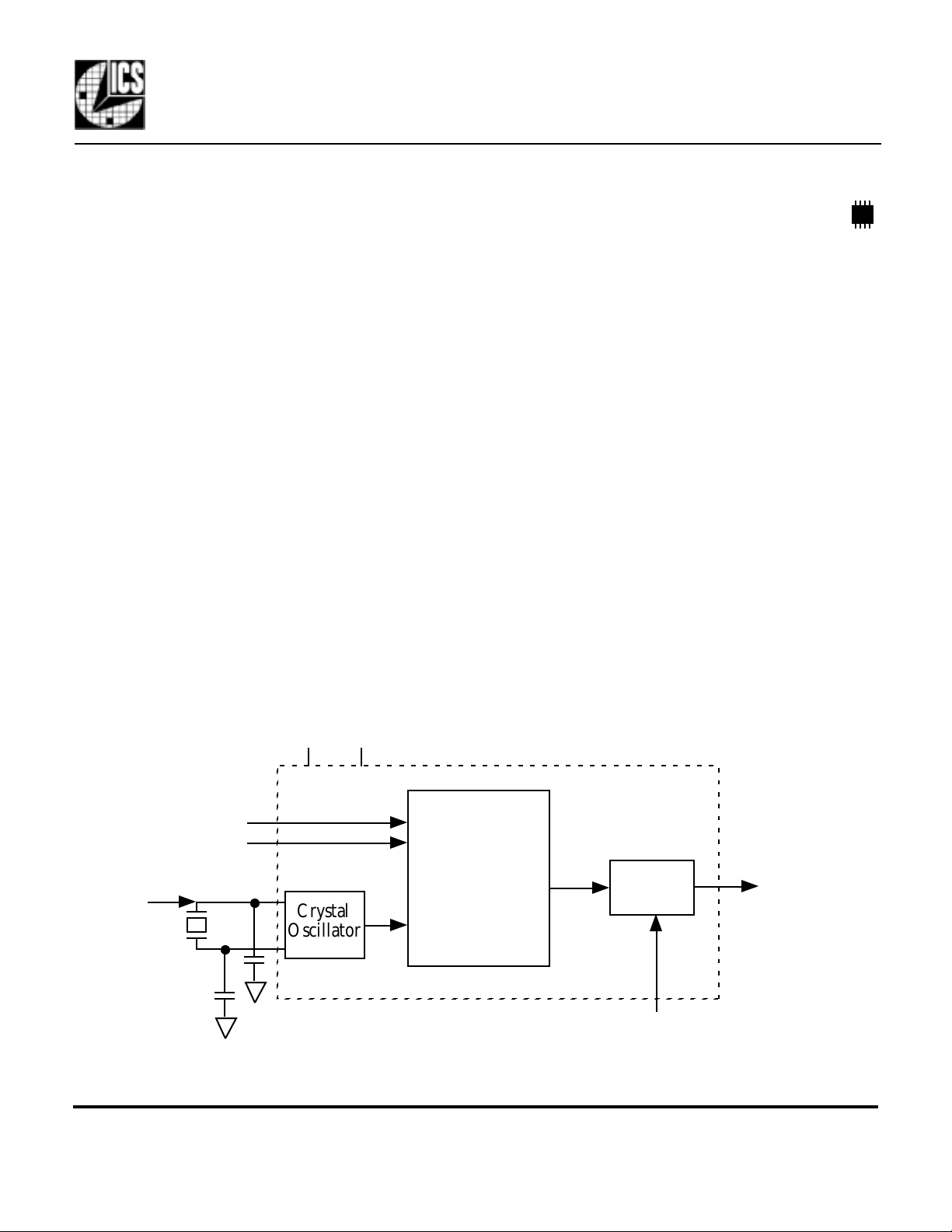
Block Diagram
Crystal or
clock in
ut
X1/ICLK
X2
VDD GND
S0
S1
Crystal
Oscillator
Optional crystal capacitors
• Industrial temperature version available
• Advanced, low power CMOS process
PLL
Clock Multiplier
Circuitry
and
ROM
Output
Buffer
Output Enable
CLK
MDS 511 C 1 Revision 061300 Printed 12/4/00
Integrated Circuit Systems, Inc. • 525 Race Street • San Jose •CA•95126•(408) 295-9800tel • www.icst.com

ICS511
g
p
LOCO™ PLL Clock Multiplier
Pin Assignment
X1/ICLK
VDD
GND
S1
18
2
3
4
X2
7
OE
6
S0
5
CLK
Clock Output Table
S1 S0 CLK
0 0 4X input
0 M 5.333X input
0 1 5X input
M 0 2.5X input
M M 2X input
M 1 3.333X input
1 0 6X input
1 M 3X input
1 1 8X input
0 = connect directly to ground.
1 = connect directly to VDD.
M = leave unconnected (floatin
).
Common Output Frequencies Examples (MHz)
Output 20 24 30 32 33.33 37.5 40 48 50 60 64
Input 10 12 10 16 16.66 15 10 12 20 10 16
Selection (S1, S0) M, M M, M 1, M M, M M, M M, 0 0, 0 0, 0 M, 0 1, 0 0, 0
Output 66.66 72 75 80 83.33 90 100 120 125 133.33 150
Input 20 12 25 10 25 15 20 15 25 25 25
Selection (S1, S0) M, 1 1, 0 1, M 1, 1 M, 1 1, 0 0, 1 1, 1 0, 1 0, M 1, 0
Note that all of the above outputs are achieved by using a common, inexpensive 10MHz to 25MHz crystal.
Consult ICS on how to achieve other out
ut frequencies.
Pin Descriptions
Number Name Type Description
1 X1/ICLK XI Crystal connection or clock input.
2 VDD P Connect to +3.3V or +5V.
3 GND P Connect to ground.
4 S1 TI Multiplier select pin 1. Connect to GND or VDD or float (no connection).
5 CLK O Clock output per Table above.
6 S0 TI Multiplier select pin 0. Connect to GND or VDD or float (no connection).
7 OE I Output Enable. Tri-states CLK output when low. Internal pull-up.
8 X2 X O Crystal connection. Leave unconnected for clock input.
Key: XI/XO = Crystal Connections, I = Input, TI = Tri-Level Input, O = output, P = power supply
connection
MDS 511 C 2 Revision 061300 Printed 12/4/00
Integrated Circuit Systems, Inc. • 525 Race Street • San Jose •CA•95126•(408) 295-9800tel • www.icst.com
 Loading...