PR EL I MI NA RY IN FO R MA TI ON
PECL to CMOS Converter
Description Features
ICS508
The ICS508 is the most cost effective way to
generate a high quality, high frequency CMOS
clock output from a PECL clock input.
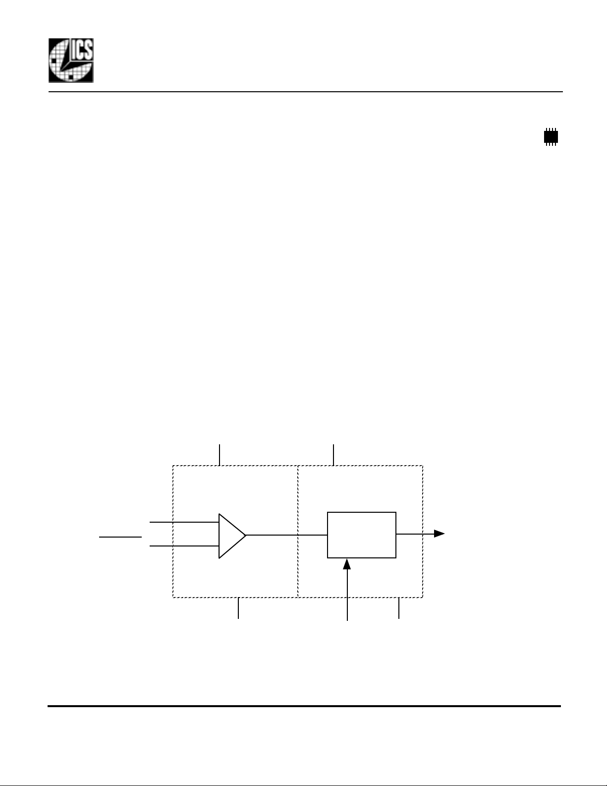
The ICS508 has separate VDD supplies for the
PECL input buffer and the output buffer allowing
different voltages to be used. For example, the
input clock could use a 3.3 V supply while the
output operates from 2.5 V.
The device has an Output Enable pin that tri-states
the clock output when the OE pin is taken low.
The ICS508 is a member of the ClockBlocks™
family of devices.
Block Diagram
• Packaged as 8 pin SOIC or die
• Separate VDD supplies allow voltage
translation
• Clock frequency of 0 - 250 MHz
• Duty cycle of 45/55
• Operating voltages of 2.375 to 5.5 V
• Tri-state output for board level testing
• 24 mA drive capability
• Industrial temperature version available
• Advanced, low power CMOS process
VDDP VDDC
PECLIN
PECLIN
GND
MDS 508 C 1 Revision 012400 Printed 11/13/00
Integrated Circuit Systems, Inc. • 525 Race Street • San Jose •CA•95126•(408) 295-9800tel • www.icst.com
Output
Buffer
OE
CLK
GND

Pin Assignment
PR EL I MI NA RY IN FO R MA TI ON
ICS508
PECL to CMOS Converter
VDDP
PECLIN
PECLIN
GND
18
2
3
4
VDDC
7
CLK
6
GND
5
OE
Pin Descriptions
Number Name Type Description
1 VDDP O Connect to 3.3 V or 5 V. Supplies PECL input buffer.
2 I Complementary PECL clock input.
3 PECLIN I
4 GND P Connect to ground.
5 OE I Output enable. Tri-states CLK output when low. Internal pull-up to VDDC.
6 GND P Connect to ground.
7 CLK O Clock output.
8 VDDC P Connect to 2.5 V, or 3.3 V or 5 V. Supplies output buffer and OE pin.
PECLIN
PECL clock input.
Key: I = Input, O = output, P = power supply connection
MDS 508 C 2 Revision 012400 Printed 11/13/00
Integrated Circuit Systems, Inc. • 525 Race Street • San Jose •CA•95126•(408) 295-9800tel • www.icst.com
 Loading...