

90C65ARevA111095
Dual Volta ge Video/ Memory Clock Gener ator
Introduction
The Integrated Circuit Systems ICS90C65 is a dual clock
generator for VGA applications. It simultaneously generates
two clocks. One clock is for the video memory, and the other
is the vide o dot clock.
The ICS90C65 has been specifically designed to serve the
por ta b le PC market with operation at ei ther 3.3 V o r 5V with a
comprehe nsiv e power - savi ng shut -do wn mode .
This data sheet supplies sales order information, a functional
overview, signal pin details, a block diagram, AC/DC characteristics, timing diagrams, and package mechanical information.
Description
The Integrated Circuit Systems Video Graphics Array Clock
Generator (ICS90C65) is capable of producing different output frequencies under firmware control. The video output
frequency is derived from a 14.318 MHz system clock available in IBM PC/XT/AT and Personal System/2 computers. It
is designed to work with Western Digital Imaging Vi deo
Graphics Array and 8514/A devices to optimize vi deo subsystem performance.
Features
•• Specified for dual voltage operation (VDD=3.3V or 5V),
but operates c ont inu ously from 3.0V to 5.25 V
•• Designed t o be powe re d-do wn for e xten de d ba tter y life
•• Backwa rd c ompa ti bilit y to the ICS90 C64 a nd IC S90C6 3
•• Dual Clock generator for the IBM-compatible Western
Digital Imagin g Vide o Gra ph ics Arra y (VGA) LSI
devices, an d 8514/A chip sets
•• Integral loop filter components, reduce cost and phase
jitt er
•• Generates fifteen video clock frequencies (including
25.175 and 28.322 MHz) derived from a 14.318 MHz
system cloc k reference frequency
•• On-chip ge ne ra tion of ei ght mem ory clo ck fre que nc ie s
•• Video clo ck is s el ectab le amo ng t he 15 in te rnal ly gene r-
ated clocks and one external clock
•• CMOS technology
•• Available in 20-pi n PL CC, SOIC and DIP pa c kage s
Integrated
Circuit
Systems, Inc.
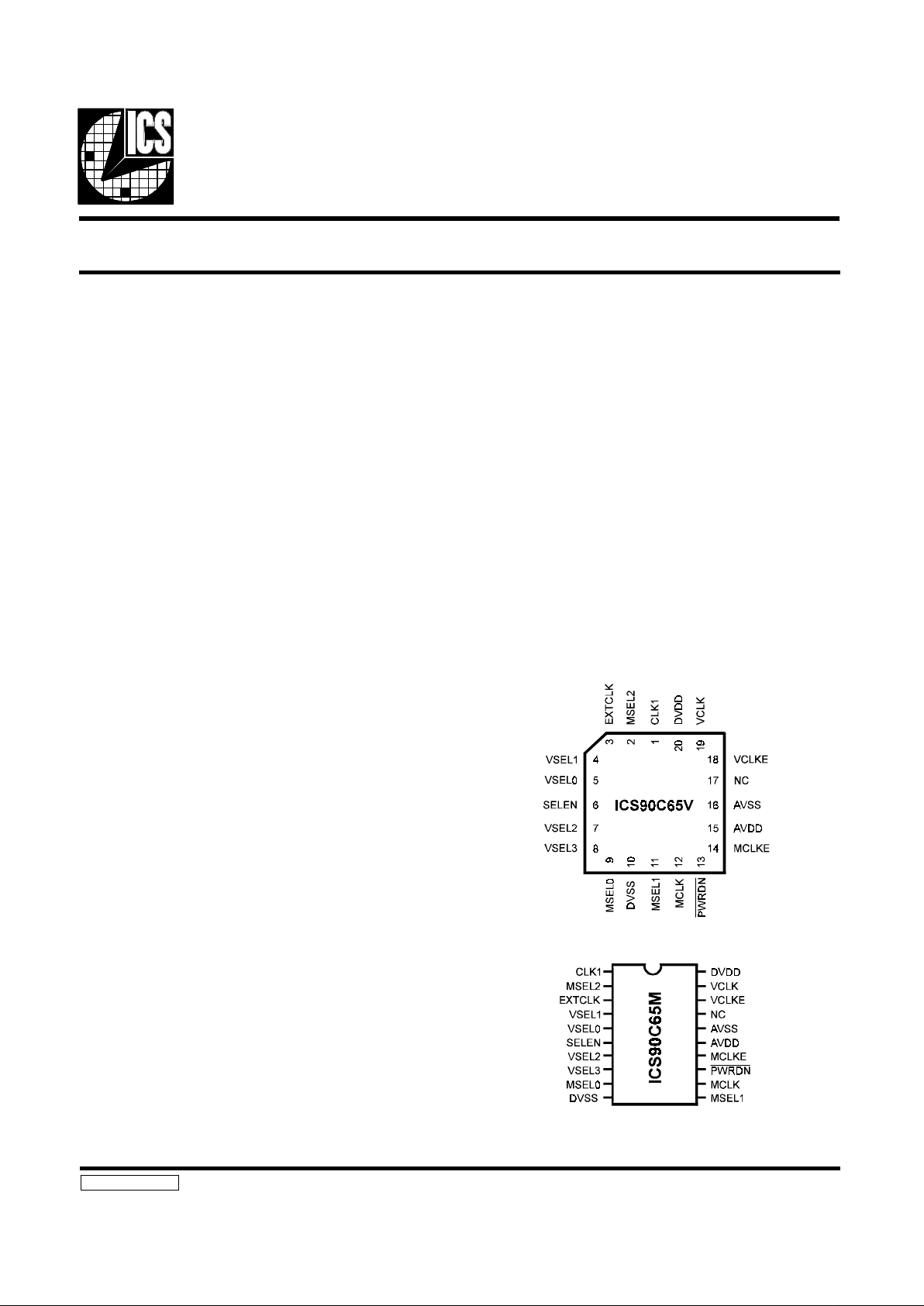
Note:ICS90C65N (DIP) pin-out is identical to ICS90C65M (SOIC) pin-out.
ICS90C 65
The video dot clock output may be one of 15 internallygener at ed fr eq uen cies or one exte rn al inpu t. T he selec ti on of
the video dot cloc k fre qu en cy is done through four inputs.
•• VSEL0
•• VSEL1
•• VSEL2
•• VSEL3
VSEL0 an d V SEL1 are lat c hed by the SEL EN signal. VS E L 2
and VSEL3 are used as direct inputs to the VCLK selection.
Table 1-1 is the truth table for VCLK selection.
The input a nd tr uth ta ble ha ve be en desi gned to allow a dire ct
connecti on t o one of th e ma ny Weste rn Digital Imagi ng V G A
controlle rs or 851 4/A chip sets.
The MCL K output is one of eight intern ally-ge nerate d frequ encies as shown in Table 1-2. The various VCLK and MCLK
frequen cies a re deri ved from the 14. 318 MHz in put fre quenc y .
The VCLKE and MCLKE input can tristate the VCLK and
MCLK output s to fa cili ta t e boar d le ve l test ing.
ICS90C65 VGA Interface
The ICS90C65 has two system interfaces: System Bus and
VGA Controll er, as well as othe r programm able in puts. Figure
1 shows how the Integrated Circuit Systems’s VGA Clock
ICS90C65 is connected to a VGA controller. Western Digital
Imaging VGA controllers normally have a status bit that indicates to the VGA cont roller that it is working with a cloc k chip.
When working with a clock chip the VGA controller changes
two of its clock inputs to outputs. They are
theVCLK1/VCSLD/VCSEL and VCLK2/VCSEL/VCSELH
outputs and they are used to select the required video frequency.
Figure 1
When the power-down capab ilit ies a re used, the co ntr ol sign al
for
PWRDN is normally held in one of a group of latches. If
the power-down function is not to be used, PWRDN must be
tied to VDD, other wise the i nternal pull-do wn will p lace the chip
in the power-down mode.
VSEL0
14.318
MHz
SD3
SD2
pull-up at reset
and PR15(5)=0
AMD(3)
VCKIN
MCLK
VCSEL
VCS
ICS90C65
WD90C26
LATCH
VSEL1
VSEL2
VCLK
MC
SELEN
CLK1
PWRDN
ICS90C65
2

Inputs from VGA Controller
The VGA controll e r inp ut t o t he ICS90C65 is:
•• SELEN
The ICS90C65 is programmed to generate different video
clock frequ encies using t he inputs of VSEL 0, VSEL1, VSE L2,
and VSEL3. The sig nals VSE L2 and VSEL 3 ma y be supplie d
by the V GA c ontroll er as is the case in W estern Digital Imagin g
VGA contr ollers. T he inputs VSEL0-1 ar e latched w ith the
signal SELEN. The SELEN input should be an active low
puls e. Thi s act ive l ow pu lse is gene rated in Western Digi tal
Imagin g VG A co ntr oll ers during I/ O wri te s to in terna l regi st er
3C2h.
Note: Only VSEL 0 and VSEL1 are latched with signal SELEN.
Outputs to VGA Controller
The outputs from th e ICS90C65 to the VGA controller are:
•• MCLK
•• VCLK
MCLK and VCLK are the two clock outputs to the VGA
controller.
User-Definable Inputs
The user de fi nable inputs are :
•• EXTCLK
•• VLCKE, MCLKE
•• MSELO-2
•• VSEL2, VSEL3
••
PWRDN
EXTCLK is an additional input that may be internally routed
to the VCLK o utput. This addi tional input is useful for supp orting modes that require frequencies not provided by the
ICS90C65 or for use during bo ar d test.
VCLKE and MCLKE a re the outpu t enable signals for VCL K
and MCLK. When low the re sp e ct iv e o utp ut i s tri sta te d.
MSEL0-2 are the memory clock (M CLK) select lines. Table 1-2 shows how MCLK frequencie s are selected. All signals
in this group ha ve internal pull-up resistors.
VSEL2 and VSEL3 are video clock (VCLK) select lines that
can select add it ion al VCL K fre qu en ci es. Se e Table 1-1.
VSEL2 and VSE L3 have internal pull-ups.
PWRDN can place the ICS90C65 in a power-down mode
which drops its suppl y current requirem ent below 1 microam p.
When placed in this mode, the digital inputs may be either high
or low or f loating withou t causing an inc rease in the ICS90C65
supply current .
The
PWRDN pin must be low (It has an internal pull-down.)
in order to place the device in its low power state. The output
pins (VCLK and MCLK) are driven high by the ICS90C65
when it is in its low power state .
If CLKI is being driven by an external source, it may be driven
low or high without a power penalty. If CLKI is at an interm ediate vo lt ag e ( V
SS
+0.5 < V
IN <VDD
-0.5) , the re wi ll be a sm all
increase in supply current. If CLKI is driven at 14.318 MHz
while the c hip is i n power -down, the ICS90C65 supp ly curre nt
will incre ase to appr oxi mat el y 1.2 mA.
The SELEN (pin 6) may be used to guard against inadvertent
frequency changes during power-down/powerup sequences.
By holding the SELEN low du ring powe r -down and powe r-u p
sequences, the ICS90C65 will retain the most recent video
frequency selection.
Analog Filters
The an alog fi lters ar e integral to the ICS90C65 device. No
external components are required. This feature reduces PC
board space re quire me nts and com ponent costs. Pha se -jitt er is
reduced as externally-generated noise cannot easily influence
the phase -locked loo p filter .
System Bus Inputs
The system bus inputs are:
•• CLKI
•• VSEL0
•• VSEL1
The ICS90C65 uses the system bus 14.318 MHz clock as a
reference to generate all its frequencies for both video and
memory clo cks. Data lines D2 and D3 are commonly used as
inputs to VSEL0 and VSE L 1 for vi de o frequ en cy selec t ion .
ICS90C65
3

Power Considerations
The ICS90C65 product requires an AVDD supply free of fast
rise time transients. This requirement may be met in several
ways and is highly depend ent on the char acter isti cs of the host
system. A VGA adapter card is unique in that it must function
in an unknown environm e nt . +5 volt po wer quali ty is depend ent not only on the quality of the power supply resident in the
host system, but also on the other cards plugged into the host’s
backplan e. Powe r suppl y noise ra nges from fai r to te rribl e. A s
the VGA adapte r manufac turer has no control ove r this, he mu st
assume the worst . The best solut ion is to crea te a clean +5 volts
by derivi ng it from th e +12 volt supply by usi ng a ze ne r di ode
and dropping resistor. A 470 Ohm resistor and 5.1 volt Zener
diode are the least costly way to accomplish this. A .047 to .1
microfarad bypass capacitor tied from AV
DD
to AvSS insures
good hig h- fre quency deco u pli ng o f thi s po int .
Laptop and notebook computers have entirely different prob-
lems with power. Typically they have no +12 volt supply;
however, they are much quieter electrically. Because the designer has complete control of the system architecture, he can
place sensitive com ponents and systems such as the RAMDAC
and Dual Video/Memory Clock away from DRAM and other
noise-generating components. Most systems provide power
that is clean enough to allow fo r jitter-free Dual Vide o/Memory
Clock performance if the +5 volt supply is decoupled with a
resistor and 22 microfarad Tantalum capacitor. Digital inputs
that are desired to be held at a static logical high level should
not be tied to +5 volts as this may result in excessive current
drain through the ESD protection diode. The internal pull-up
resistors will adequately kee p thes e inputs high.
ICS90C65
4

Pin Descriptions
The following table provides the pin descriptions for the 20-pin ICS90C65 packages.
PIN
NUMBER
PIN
SYMBOL TYPE DESCRIPTION
1 CLKI IN Reference input cloc k fro m system .
2 MSEL2 IN Select inp ut for MCL K sele c tion.
3 EXTCLK IN Externa l cloc k inp ut fo r an addit ion al fre que nc y.
4 VSEL1 IN Control inp ut for VCL K selection.
5 VSEL0 IN Control inp ut for VCL K selection.
6 SELEN IN Strobe for latchin g VSEL( 0,1) (low enab le ).
7 VSEL2 IN Control inp ut for VCL K selection.
8 VSEL3 IN Control inp ut for VCL K selection.
9 MSEL0 IN Select inp ut for MCL K sele c tion.
10 DVSS - Ground for Di git a l Ci rc uit .
11 MSEL1 IN Select input for MCL K sele cti on.
12 MCLK OUT Memory Clock Output.
13
PWRDN IN Power Down Control.
14 MCLKE IN Enable input fo r MCLK o utp ut (h igh ena ble s out put).
15 AVDD - Power supply for ana log circ ui t.
16 AVSS - Ground for analog circuit.
17 NC - No connec ti on.
18 VCLKE IN Enable input for VCLK outpu t (high enables output).
19 VCLK OUT Vide o Cloc k Output.
20 DVDD - Power supply for Digit a l Ci rc uit .
Note:
CLKI, EXTCL K,VSEL0, VSEL1,VSE L2, VSEL3, SELEN, MSEL 0, MSEL1, MSEL2, VCL KE, and MC LKE - input pins have
internal pull-up resistors.
PWRDN has an interna l pull-down resistor.
ICS90C65
5

Absolute Maximum Ratings
Ambient Temperature
under bia s
0°C to 70°C
Storage tempera t ure -40°C to 125°C
Voltage on all inputs and
outputs with respect to V
SS
0.3 to 7 vo lts
Note: Stresses above those listed under Absolute Maximum
Ratings may cause permanent damage to the device. This is a
stress rating only and func tional op eration of t he device at these
or any other conditions abov e those indic ated in the opera tional
sections of t he spec ificat ions is not implied. Exp osure to ab solute maximum rating conditions for extended periods may
affect product reliability.
Standard Test Conditions
The ch arac t eristi c s bel ow a pp ly for the f oll owi ng st an dard te st
conditions, unless otherwise noted. All volt ages are re ference d
to V
SS
(OV Ground). Positive current flows into th e refer-
enced pin.
Operating T emperature
range
0°C to 70°C
Power supply voltage 3. 0 to 5.25 volts
SYMBOL PARAMETER MIN MAX NOTES
STROBE TIMING
Tpw
Tsu
Thd
Strobe Pulse Widt h
Setup Time Data to Str obe
Hold Ti m e Dat a to Strobe
20
20
10
-
-
-
MCLK and VCLK TIMINGS @ 5.0V
Tr
Tf
-
-
-
-
Rise Time
Fall Time
Freq uency Error
Maximum Frequency
Propaga tion De lay f or Pas s Through
Frequency
Outpu t Ena bl e to Tristate
(into and out of) time
-
-
-
2
2
0.5
135
20
15
Duty Cycle 40% m in. to
60% max.
%
MHz
ns
ns
MCLK and VCLK TIMINGS @ 3.3V
Tr
Tf
-
-
-
-
Rise Time
Fall Time
Freq uency Error
Maximum Frequency
Propaga tion De lay f or Pas s Through
Frequency
Outpu t Ena bl e to Tristate
(into and out of) time
-
-
-
3
3
.5
110
30
20
Duty Cycle 40% m in. to
60% max.
%
MHz
ns
ns
AC Timing Characteristics
The following notes apply to all of the parameters presented in this section:
1. REFCLK = 14.318 MHz
2. T
C
= 1/F
C
3. All units are in nanose c onds (ns).
4. Maximum jitter is within a range of 30 µs after triggering on a 400 MHz sco pe.
5. Rise and fall time is between 0.8 and 2.0 VDC unless otherwise stated.
6. Output pin loading = 15pF
7. Duty cycle is measured at V
DD
/2 unless otherwise stated.
ICS90C65
6

DC Characteristics at 5 Volts VDD
SYMBOL PARAMETER MIN MAX UNITS CONDITIONS
V
DD
Operating Voltage Range 4.75 5.25 V
V
IL
Input Low Vo lt ag e V
SS
0.8 V V
DD =
5V
V
IH
Input High Vo ltag e 2.0 V
DD
VV
DD
= 5V
I
IH
Input L e ak ag e Current - 10
µA
VIN = V
CC
V
OL
Output Low Voltage - 0.4 V IOL = 8.0 m A
V
OH
Output High Voltage 2.4 - V IOH = 8.0 mA
I
DD
Supply Current - 30 mA VDD = 5V
R
UP
Internal Pul l- up Resisto r s 50 - K ohms VIN = 0.0V
C
in
Input Pin Capaci ta nc e - 8 pF FC = 1 MHz
C
out
Output Pin Capa cit an ce - 12 pF FC = 1 MHz
I
PN
Power-do wn Suppl y Curre nt - 1.0
µA
VDD=3.3V
R
DN
Internal Pul l- down Equivalent 20 - K ohms VIN=VDD=5V
DC Characteristics at 3.3 Volts V
DD
SYMBOL PARAMETER MIN MAX UNITS CONDITIONS
V
DD
Operating Voltage Range 3.0 3.6 V
V
IL
Input Low Vol tage V
SS
0.8 V VDD = 3.3V
V
IH
Input High Vol tage 2.0 V
DD
VV
DD
= 3.3V
I
IH
Input Leakage Curre nt - 10
µA
Vin = V
DD
V
OL
Output Low Vo lt ag e - 0.4 V IOL = 3.0 mA
V
OH
Output High Vo ltag e 2.4 - V IOH = 3.0 mA
I
DD
Supply Current - 20 mA VDD = 3.3V
R
UP
Internal Pul l-u p Resistor s 100 - K ohms VIN = 0.0V
C
in
Input Pin Capacitanc e - 8 pF FC = 1 MHz
C
out
Output Pin Capacitanc e - 12 pF FC = 1 MHz
I
PN
Power-down Supply Current - 1.0
µA
VDD =3.3V
R
DN
Internal Pul l-d own Equivalent 50 - K ohms VIN =VDD =3.3V
ICS90C65
7

ICS90C65 Timing
ICS90C65
8

VSEL
3210
VCLK FREQUENCY (MHz)
Pattern 951
0
0
0
0
0
0
0
0
0
0
1
1
0
1
0
1
30.0
77.25
EXTCLK
80.0
0
0
0
0
1
1
1
1
0
0
1
1
0
1
0
1
31.5
36.0
75.0
50.0
1
1
1
1
0
0
0
0
0
0
1
1
0
1
0
1
40.0
50.0
32.0
44.9
1
1
1
1
1
1
1
1
0
0
1
1
0
1
0
1
25.175
28.322
65.0
36.0
MSEL
210
MCLK FREQUENCIE S (MHz )
Pattern 951
0
0
0
0
0
0
1
1
0
1
0
1
33.0
49.218
60.0
30.5
1
1
1
1
0
0
1
1
0
1
0
1
41.612
37.5
36.0
44.296
T ab le 1-1 VCLK SELECTION
T ab le 1-2 MCLK SELECTION
ICS90C65
9

20-Pin D IP Pack age 20-Pin SOI C Pack age
PLCC Package
Ordering Information
ICS90C65N or ICS90C65M or ICS90C65V
Example:
ICS XXXX- XXX N
Package Type
N=DIP (Plastic) V=PLCC
M=SOIC
Pattern Number (2 or 3 digit number for parts with ROM code patterns)
Device Type (consi st s of 3-6 digi t nu mb er s)
Prefix
ICS, AV=Standard Device; GSP=Genlock Device
ICS90C65
10
 Loading...