

Integrated
Circuit
Systems, Inc.
ICS9250-29
Third party brands and names are the property of their respective owners.
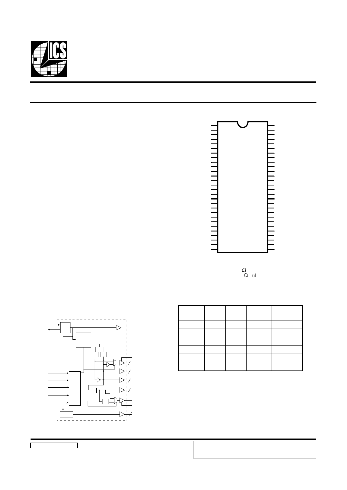
Block Diagram
9250-29 Rev A 02/01/01
Recommended Application:
Solano type chipset.
Output Features:
• 2 CPU (2.5V) (up to 133MHz achievable through I
2
C)
• 13 SDRAM (3.3V) (up to 133MHz achievable
through I
2
C)
• 5 PCI (3.3 V) @33.3MHz
• 1 IOAPIC (2.5V) @ 33.3 MHz
• 3 Hublink clocks (3.3 V) @ 66.6 MHz
• 2 (3.3V) @ 48 MHz (Non spread spectrum)
• 1 REF (3.3V) @ 14.318 MHz
Features:
• Supports spread spectrum modulation,
0 to -0.5% down spread.
•I
2
C support for power management
• Efficient power management scheme through PD#
• Uses external 14.138 MHz crystal
• Alternate frequency selections available through I
2
C
control.
Functionality
Pin Configuration
56-Pin 300mil SSOP
* This input has a 50KW pull-down to GND.
** This input has a 50KW pull-up to VDD
IOAPIC
VDDL
GNDL
*FS1/REF
VDDR
X1
X2
GNDR
VDD3
3V66-0
3V66-1
3V66-2
GND3
PCICLK0
PCICLK1
PCICLK2
VDD2
GND2
PCICLK3
PCICLK4
FS0
GNDA
VDDA
SCLK
S DATA
GNDF
VDDF
48MHz_0
GNDL
VDDL
CPUCLK0
CPUCLK1
GND1
SDRAM0
SDRAM1
VDD1
GND1
SDRAM2
SDRAM3
SDRAM4
SDRAM5
VDD1
GND1
SDRAM6
SDRAM7
SDRAM8
SDRAM9
VDD1
GND1
SDRAM10
SDRAM11
VDD1
GND1
SDRAM12
TRISTATE#/PD#**
48MHz_1
ICS9250-29
1
2
3
4
5
6
7
8
9
10
11
12
13
14
15
16
17
18
19
20
21
22
23
24
25
26
27
28
56
55
54
53
52
51
50
49
48
47
46
45
44
43
42
41
40
39
38
37
36
35
34
33
32
31
30
29
Frequency Generator & Integrated Buffers for Celeron & PII/III™
REF
CPU66/100/133 [1:0]
VDDL
3V66 [2:0]
SDRAM [12:0]
PCICLK [4:0]
IOAPIC
VDDL
PLL2
48MHz [1:0]
X1
X2
XTAL
OSC
Control
Logic
Config
Reg
FS(1:0)
PD#
TRISTATE#
2
2
3
13
5
/2
/2
/3
/2
PLL1
Spread
Spectrum
SDATA
SCLK
#etatsirT0SF1SF
UPC
zHM
MARDS
zHM
00X etatsirTetatsirT
01XtseTtseT
100 zHM66zHM001
110 zHM001zHM001
101 zHM331zHM331
111 zHM331zHM001
ICS reserves the right to make changes in the device data identified in this
publication without further notice. ICS advises its customers to obtain the
latest version of all device data to verify that any information being relied
upon by the customer is current and accurate.
Power Groups
VDDA, GNDA = CPU, PLL (analog)
VDDF, GNDF = Fixed PLL, 48M (analog/digital)
VDDR, GNDR = REF, X1, X2 (analog/digital)
VDD3, GND3 = 3V66 (digital)
VDD2, GND2 = PCI (digital)
VDD1, GND1 = SDRAM (digital)
VDDL, GNDL = IOAPIC, CPU (digital)
2
ICS9250-29
The ICS9250-29 is a single chip clock solution for Solano type chipset. It provides all necessary clock signals for such
a system.
Spread spectrum may be enabled through I
2
C programming. Spread spectrum typically reduces EMI by 8dB to 10 dB.
This simplifies EMI qualification without resorting to board design iterations or costly shielding. The ICS9250-29
employs a proprietary closed loop design, which tightly controls the percentage of spreading over process and
temperature variations.
General Description
Pin Configuration
REBMUNNIPEMANNIPEPYTNOITPIRCSED
1CIPAOITUO.zHM3.33tagninnurtuptuokcolcV5.2
55,2LDDVRWPCIPAOI&UPCrofylppusrewopV5.2
65,3LDNGRWPCIPAOI&UPCrofylppusrewopV5.2rofdnuorG
4
1SFNIytilanoitcnuftuptuolla,ycneuqerfUPCsenimreteD.niptceleSnoitcnuF
FERTUO.tuptuokcolcecnereferzHM813.41,V3.3
,72,32,71,9,5
94,34,73,33
xDDVRWPylppusrewopV3.3
61XNI
kcabdeefdna)Fp33(pacdaollanretnisah,tupnilatsyrC
2Xmorfrotsiser
72XTUO
daollanretnisaH.zHM813.41yllanimon,tuptuolatsyrC
)Fp33(pac
,62,22,81,31,8
25,84,24,63,23
xDNGRWPylppusV3.3rofsnipdnuorG
01,11,21)0:2(66V3TUOBUHrofstuptuokcolczHM66dexiFV3.3
120SFNI.ytilanoitcnuftuptuolla,ycneuqerfUPCsenimreteD.niptceleSnoitcnuF
41,51,61,91,02)0:4(KLCICPTUOstuptuokcolcICPV3.3
03
#ETATSIRTNI
#ETATSIRTehtotstluafednip#DP/#ETATSIRTehtpurewoptA
derahSees(.sedomTSETdna#ETATSIRTehtelbaneotnoitcnuftupni
.)noitpircsedllufrofnoitarepOniP
#DPNI
otniecivedehtnwodrewopotdesuniptupniwolevitcasuonorhcnysA
dnaOCVehtdnadelbasideraskcolclanretniehT.etatsrewopwola
ebtonlliwnwodrewopehtfoycnetalehT.deppotseralatsyrceht
.sm3nahtretaerg
42KLCSNIIfotupnikcolC
2
tupniC
52ATADSNIIroftupniataD
2
.tupnilairesC
82,92)0:1(zHM84TUO.stuptuokcolczHM84dexiFV3.3
,83,53,43,13
,44,14,04,93
15,05,74,64,54
MARDS
]0:21[
TUO
nacstuptuoMARDSllA.zHM331dnazHM001gninnurtuptuoV3.3
Ihguorhtffodenruteb
2
C
45,35)0:1(KLCUPCTUO
gnidnepedzHM331rozHM001,zHM66.tuptuokcolcsubtsoHV5.2
.snipSFno
3
ICS9250-29
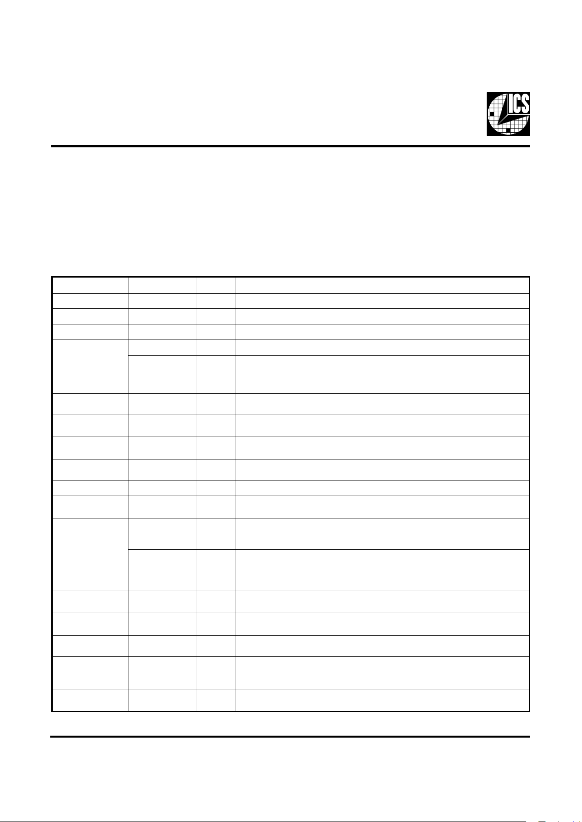
Power Down Waveform
Note
1. After PD# is sampled active (Low) for 2 consective rising edges of CPUCLKs, all the
output clocks are driven Low on their next High to Low tranistiion.
2. Power-up latency <3ms.
3. Waveform shown for 100MHz
Maximum Allowed Current
Clock Enable Configuration
#DPKLCUPCMARDSCIPAOI66V3KLCICP
,FER
zHM84
csOsOCV
0WOLWOLWOLWOLWOLWOLFFOFFO
1NONONONONONONONO
onaloS
noitidnoC
noitpmusnocylppusV5.2xaM
,sdaolpacetercsidxaM
V526.2=2qddV
DNGro3qddV=stupnicitatsllA
noitpmusnocylppusV3.3xaM
,sdaolpacetercsidxaM
V564.3=3qddV
DNGro3qddV=stupnicitatsllA
edoMnwodrewoP
)0=#NWDRWP(
Am2Am2
zHM66evitcAlluF
00=)0:1(SF
Am53Am044
zHM001evitcAlluF
10=)0:1(SF
Am05Am034
zHM331evitcAlluF
11=)0:1(SF
Am06Am044
zHM331evitcAlluF
01=)0:1(SF
Am06Am005
4
ICS9250-29
1. The ICS clock generator is a slave/receiver, I2C (SMB) component. It is only a "write" mode SMB device, no readback on
this part. Read-Back will lock up the PIIX-4 due to the Byte count of 00
H
.
2. The data transfer rate supported by this clock generator is 100K bits/sec or less (standard mode)
3. The input is operating at 3.3V logic levels.
4. The data byte format is 8 bit bytes.
5. To simplify the clock generator I
2
C interface, the protocol is set to use only "Block-Writes" from the controller. The bytes
must be accessed in sequential order from lowest to highest byte with the ability to stop after any complete byte has been
transferred. The Command code and Byte count shown above must be sent, but the data is ignored for those two bytes. The
data is loaded until a Stop sequence is issued.
6. At power-on, all registers are set to a default condition, as shown.
General I2C serial interface information
The information in this section assumes familiarity with I2C programming.
For more information, contact ICS for an I
2
C programming application note.
How to Write:
• Controller (host) sends a start bit.
• Controller (host) sends the write address D2
(H)
• ICS clock will acknowledge
• Controller (host) sends a dummy command code
• ICS clock will acknowledge
• Controller (host) sends a dummy byte count
• ICS clock will acknowledge
• Controller (host) starts sending first byte (Byte 0) through byte 5
• ICS clock will acknowledge each byte one at a time.
• Controller (host) sends a Stop bit
Notes:
Controller (Host) ICS (Slave/Receiver)
Start Bit
Address
D2
(H)
A
CK
Dummy Command Code
A
CK
Dummy Byte Count
A
CK
Byte 0
A
CK
Byte 1
ACK
Byte 2
A
CK
Byte 3
A
CK
Byte 4
A
CK
Byte 5
A
CK
Stop Bit
How to Write:
Note: This clock does not support Read Back. Doing a
read back will lock up the PIIX-4 system.
5
ICS9250-29
etatsirT0SF1SFUPCMARDS66V3ICPzHM84FERCIPAOI
00X etatsirTetatsirTetatsirTetatsirTetatsirTetatsirTetatsirT
01X 2/KLCT2/KLCT3/KLCT6/KLCT2/KLCTKLCT6/KLCT
100 zHM6.66zHM001zHM6.66zHM3.33zHM84zHM813.41zHM3.33
110 zHM001zHM001zHM6.66zHM3.33zHM84zHM813.41zHM3.33
101 zHM331zHM331zHM6.66zHM3.33zHM84zHM813.41zHM3.33
111 zHM331zHM001zHM6.66zHM3.33zHM84zHM813.41zHM3.33
Truth Table
Byte 0: Control Register
(1 = enable, 0 = disable)
Byte 1: Control Register
(1 = enable, 0 = disable)
tiB#niPemaNDWPnoitpircseD
7tiB- )DIdevreseR(0)evitcanI/evitcA(
6tiB- )DIdevreseR(0)evitcanI/evitcA(
5tiB- )DIdevreseR(0)evitcanI/evitcA(
4tiB- )DIdevreseR(1)evitcanI/evitcA(
3tiB- murtcepSdaerpS0)ffO=0/nO=1(
2tiB921_zHM841)evitcanI/evitcA(
1tiB820_zHM841)evitcanI/evitcA(
0tiB- )DIdevreseR(0)evitcanI/evitcA(
tiB#niPemaNDWPnoitpircseD
7tiB047MARDS1)evitcanI/evitcA(
6tiB146MARDS1)evitcanI/evitcA(
5tiB445MARDS1)evitcanI/evitcA(
4tiB544MARDS1)evitcanI/evitcA(
3tiB643MARDS1)evitcanI/evitcA(
2tiB742MARDS1)evitcanI/evitcA(
1tiB051MARDS1)evitcanI/evitcA(
0tiB150MARDS1)evitcanI/evitcA(
Note:
Reserved ID bits must be written with "0"

6
ICS9250-29
Byte 2: Control Register
(1 = enable, 0 = disable)
Notes:
1. Inactive means outputs are held LOW and are disabled from switching. These outputs are designed to be configured at
power-on and are not expected to be configured during the normal modes of operation.
2. PWD = Power on Default
3. Undefined bits can be written with either "1" or "0"
tiB#niPemaNDWPnoitpircseD
7tiB21)PGA(2_66V31)evitcanI/evitcA(
6tiB1321MARDS1)evitcanI/evitcA(
5tiB4311MARDS1)evitcanI/evitcA(
4tiB5301MARDS1)evitcanI/evitcA(
3tiB839MARDS1)evitcanI/evitcA(
2tiB938MARDS1)evitcanI/evitcA(
1tiB511KLCICP1)evitcanI/evitcA(
0tiB- tibdenifednU0 )evitcanI/evitcA(
Byte 3: ICS Reserved Functionality and frequency select register (Default as noted in PWD)
Note 1: For system operation, the BSEL lines of the CPU will program FS0, FS1 for the appropriate CPU speed, always with
SDRAM = 100MHz. After BIOS verifies the SDRAM is PC133 speed, then bit 0 can be written from the default 0 to 1
to change the SDRAM output frequency from 100MHz to 133MHz. This will only change if the CPU is at the
133MHz FSB speed as shown in this table. The CPU, 3V66, PCI and IOAPIC clocks will be glitch free during this
transition, and only SDRAM will change.
Note 2: Must be written with "0"
Note 3: Undefined bits can be written with either "1" or "0"
tiBnoitpircseDDWP
7tiB)2etoN(tibdevreseRSCI 0
6tiB)2etoN(tibdevreseRSCI 0
5tiB)2etoN(tibdevreseRSCI 0
4tiB)2etoN(tibdevreseRSCI 0
3tiB)lamron=0/%5=1(edomkcolcrevo%5 0
2tiB)3eton(tibdenifednU 1
1tiBnoitpircsednipees)#etatsirT=0/#NDRWP=1(#NDRWP/#etatsirT 1
0tiB
0tiB1SF0SF
KLCUPC
zHM
MARDS
zHM
66V3
zHM
KLCICP
zHM
CIPAOI
zHM
0
1etoN
000 66.660.00166.6633.3333.33
001 0.0010.00166.6633.3333.33
010 23.33123.33166.6633.3333.33
011 23.3310.00166.6633.3333.33
100 66.660.00166.6633.3333.33
10 1 0.0010.00166.6633.3333.33
110 23.33123.33166.6633.3333.33
111 23.33123.33166.6633.3333.33

7
ICS9250-29
Byte 4: Reserved Register
(1 = enable, 0 = disable)
Byte 5: Reserved Register
(1 = enable, 0 = disable)
tiB#niPemaNDWPnoitpircseD
7tiB- )devreseR(0)evitcanI/evitcA(
6tiB- )devreseR(0)evitcanI/evitcA(
5tiB- )devreseR(0)evitcanI/evitcA(
4tiB- )devreseR(0)evitcanI/evitcA(
3tiB- )devreseR(0)evitcanI/evitcA(
2tiB024KLCICP1)evitcanI/evitcA(
1tiB913KLCICP1)evitcanI/evitcA(
0tiB612KLCICP1)evitcanI/evitcA(
tiB#niPemaNDWPnoitpircseD
7tiB- )devreseR(0)evitcanI/evitcA(
6tiB- )devreseR(0)evitcanI/evitcA(
5tiB- )devreseR(0)evitcanI/evitcA(
4tiB- )devreseR(0)evitcanI/evitcA(
3tiB- )devreseR(0)evitcanI/evitcA(
2tiB- )devreseR(0)evitcanI/evitcA(
1tiB- )devreseR(0)evitcanI/evitcA(
0tiB- )devreseR(0)evitcanI/evitcA(
Notes:
1. Inactive means outputs are held LOW and are disabled from switching. These outputs are designed to be configured at
power-on and are not expected to be configured during the normal modes of operation.
2. PWD = Power on Default

8
ICS9250-29
Absolute Maximum Ratings
Core Supply Voltage . . . . . . . . . . . . . . . . . . . . . . . . 4.6 V
I/O Supply Voltage . . . . . . . . . . . . . . . . . . . . . . . . . 3.6V
Logic Inputs . . . . . . . . . . . . . . . . . . . . . . . . . . . . . . . GND –0.5 V to V
DD
+0.5 V
Ambient Operating Temperature . . . . . . . . . . . . . . 0°C to +70°C
Storage Temperature . . . . . . . . . . . . . . . . . . . . . . . . –65°C to +150°C
Stresses above those listed under Absolute Maximum Ratings may cause permanent damage to the device. These ratings are stress
specifications only and functional operation of the device at these or any other conditions above those listed in the operational sections
of the specifications is not implied. Exposure to absolute maximum rating conditions for extended periods may affect product
reliability.
Electrical Characteristics - Input/Supply/Common Output Parameters
TA = 0 - 70C; Supply Voltage VDD = 3.3 V +5%, VDDL=2.5 V+ 5%(unless otherwise stated)
PARAMETER SYMBOL CONDITIONS MIN TYP MAX UNITS
Input High Voltage V
IH
2V
DD
+0.3 V
Input Low Voltage V
IL
VSS-0.3 0.8 V
Input High Current I
IH
VIN = V
DD
-5 5
µ
A
Input Low Current I
IL1
VIN = 0 V; Inputs with no pull-up resistors -5
µ
A
Input Low Current I
IL2
VIN = 0 V; Inputs with pull-up resistors -200
µ
A
Operating I
DD3. 3OP
CL = 0 pF; Select @ 66M 100 mA
Supply Current
Power Do wn I
DD3. 3PD
CL = 0 pF; With input address to Vdd or GND 600
µ
A
Supply Current
Input frequency F
i
VDD = 3.3 V; 14.318 MHz
Pin Inductance
1
L
pin
7nH
C
IN
Logic Inputs 5 pF
C
out
Out put pin capacitance 6 pF
C
INX
X1 & X2 pins 13.5 22.5 pF
Transition Time
1
T
trans
To 1st crossing of target Freq. 3 ms
Settling Time
1
T
s
From 1st crossing to 1% target Freq. 3 ms
Clk Stabilization
1
T
STAB
From VDD = 3.3 V to 1% target Freq. 3 ms
t
PZH,tPZH
output enable delay (all outputs) 1 10 ms
t
PLZ,tPZH
output disable delay (all outputs) 1 10 ms
1
Guarenteed by design, not 100% tested in production.
Delay
1
Input Capacitance
1
Group Timing Relationship Table
1
puorGzHM66UPC
zHM001MARDS
zHM001UPC
zHM001MARDS
zHM331UPC
zHM001MARDS
zHM331UPC
zHM331MARDS
tesffOecnareloTtesffOecnareloTtesffOecnareloTtesffOecnareloT
MARDSotUPCsn5.2-sp005sn0.5sp005sn0.0sp005sn57.3sp005
66V3otUPCsn5.7sp005sn0.5sp005sn0.0sp005sn0.0sp005
66V3otMARDSsn0.0sp005sn0.0sp005sn0.0sp005sn57.3-sp005
ICPot66V3sn5.3-5.1sp005sn5.3-5.1sp005sn5.3-5.1sp005sn5.3-5.1sp005
CIPAOIotICPsn0.0sn1sn0.0sn1sn0.0sn1sn0.0sn1
TOD&BSUhcnysAA/NhcnysAA/NhcnysAA/NhcnysAA/N

9
ICS9250-29
Electrical Characteristics - 3V66
TA = 0 - 7 0C; VDD = 3.3 V +/-5%; V
DDL
= 2.5 V +/-5%;CL = 10-30 pF (unless otherwise stated)
PARAMETER SYMBOL CONDITIONS MIN TYP MAX UNITS
Output Impedance R
DSP1
1
VO = VDD*(0.5) 12 55
Ω
Output Impedance R
DSN1
1
VO = VDD*(0.5) 12 55
Ω
Output Hi g h Vo l t age V
OH1
IOH = -1 mA 2.4 V
Output Low Vo l t age V
OL1
IOL = 1 mA 0.4 V
Output High Current I
OH1
VOH@ MIN = 1 .0 V, VOH@ MAX = 3.135 V-33 -33 mA
Output Low Current I
OL1
VOL@ MIN = 1.95 V, VOL@ MAX= 0.4V 30 38 mA
Rise Time t
r1
1
VOL = 0.4 V, VOH = 2.4 V 0.5 1.46 2 ns
Fall Time t
f1
1
VOH = 2.4 V, VOL = 0.4 V 0.5 1.47 2 ns
Duty Cycle d
t1
1
VT = 1.5 V 45 50.2 55 %
Skew t
sk1
1
VT = 1.5 V 175 ps
Jitter
t
jcyc-cyc
1
VT = 1.5 V
500 ps
1
Guarenteed by design, not 100% tested in production.
Electrical Characteristics - CPU
TA = 0 - 7 0C, VDD=3,3V +/-5%, V
DDL
= 2.5 V +/-5%; CL = 10 - 20 pF (unless otherwise stated)
PARAMETER SYMBOL CONDITIONS MIN TYP MAX UNITS
Output Impedance R
DSP2B
1
VO = VDD*(0.5) 13.5 45
Ω
Output Impedance R
DSN2 B
1
VO = VDD*(0.5) 13.5 45
Ω
Output Hi g h Vo l t age V
OH2 B
IOH = -1 mA 2 V
Output Lo w Vo l t age V
OL2 B
IOL = 1 mA 0.4 V
Output High Current I
OH2 B
V
OH @MIN
= 1.0V , V
OH@ MA X
= 2.375V -27 -27 mA
Output Low Current I
OL2 B
V
OL @MIN
= 1.2V , V
OL@ MAX
= 0.3V 27 30 mA
Rise Time t
r2B
1
VOL = 0.4 V, VOH = 2.0 V 0.4 1.10 1.6 ns
Fall Time t
f2B
1
VOH = 2.0 V, VOL = 0.4 V 0.4 1.26 1.6 ns
Dut y Cycle d
t2B
1
VT = 1.25 V 45 53.6 55 %
Skew t
sk2B
1
VT = 1.25 V 175 ps
Jitter
t
jcyc-cyc
1
VT = 1.25 V
250 ps
1
Guarenteed by design, not 100% tested in production.

10
ICS9250-29
Electrical Characteristics - IOAPIC
TA = 0 - 7 0C; VDD = 3.3 V +/-5%, V
DDL
= 2.5 V +/-5%; CL = 10 - 20 pF (unless otherwise stated)
PARAMETER SYMBOL CONDITIONS MIN TYP MAX UNITS
Output Impedance R
DSP4B
1
VO = VDD*(0.5) 9 30
Ω
Output Impedance R
DSN4 B
1
VO = VDD*(0.5) 9 30
Ω
Output Hi g h Vo l t a g e V
OH4 B
IOH = -1 mA 2 V
Output Lo w Vo l t age V
OL4 B
IOL = 1 mA 0.4 V
Output High Current I
OH4 B
V
OH@ mi n
= 1.0 V, V
OH@ MA X
= 2.375 V -27 -27 mA
Output Low Current I
OL4 B
V
OL@ MIN
= 1.2 V, V
OL@ MAX=
0.3V 27 30 mA
Rise Time t
r4B
1
VOL = 0.4 V, VOH = 2.0 V 0.4 1.09 1.6 ns
Fall Time t
f4B
1
VOH = 2.0 V, VOL = 0.4 V 0.4 1.22 1.6 ns
Dut y Cycle d
t4B
1
VT = 1.25 V 45 50.2 55 %
Jitter
t
jcyc-cyc
1
VT = 1.25 V
500 ps
1
Guarenteed by design, not 100% tested in production.
Electrical Characteristics - SDRAM
TA = 0 - 7 0C; VDD = 3.3 V +/-5%, V
DDL
= 2.5 V +/-5 %, CL = 20 - 30 pF (unless otherwise stated)
PARAMETER SYMBOL CONDITIONS MIN TYP MAX UNITS
Output Impedance R
DSP3
1
VO = VDD*(0.5) 10 24
Ω
Output Impedance R
DSN3
1
VO = VDD*(0.5) 10 24
Ω
Output Hi g h Vo l t age V
OH3
IOH = -1 mA 2.4 V
Output Low Vo ltage V
OL3
IOL = 1 mA 0.4 V
Output High Current I
OH3
V
OH @MIN
= 2.0 V, V
OH@ MA X
=3.135 V -54 -46 mA
Output Low Current I
OL3
V
OL@ MIN
= 1.0 V, V
OL@ MAX
=0.4 V 49 53 mA
Rise Time t
r3
1
VOL = 0.4 V, VOH = 2.4 V 0.4 1.19 1.6 ns
Fall Time t
f3
1
VOH = 2.4 V, VOL = 0.4 V 0.4 1.43 1.6 ns
Dut y Cycle d
t3
1
VT = 1.5 V 45 54.9 55 %
Skew t
sk3
1
VT = 1.5 V 250 ps
Jitter
t
j
cyc-cyc1VT = 1.5 V
250 ps
1
Guarenteed by design, not 100% tested in production.

11
ICS9250-29
Electrical Characteristics - PCI
TA = 0 - 70 C; VDD = 3.3 V +/-5%, V
DDL
= 2.5 V +/-5%; CL = 10-30 pF (unless otherwise stated)
PARAMETER SYMBOL CONDITIONS MIN TYP MAX UNITS
Output Impedance R
DSP1
1
VO = VDD*(0.5) 12 55
Ω
Output Impedance R
DSN1
1
VO = VDD*(0.5) 12 55
Ω
Outpu t Hi g h Volt age V
OH1
IOH = -1 mA 2.4 V
Outpu t Low Voltag e V
OL1
IOL = 1 mA 0.4 V
Outpu t Hi g h Curre nt I
OH1
V
OH@ MIN
= 1.0 V, V
OH@ MAX
= 3.135 V -33 -33 mA
Outpu t Lo w Curren t I
OL1
V
OL@ MIN
= 1.95 V, V
OL@ MAX
= 0.4 30 38 mA
Rise Time t
r1
1
VOL = 0.4 V, VOH = 2.4 V 0.5 1.43 2 ns
Fal l Ti me t
f1
1
VOH = 2.4 V, VOL = 0.4 V 0.5 1.63 2 ns
Duty Cy cle d
t1
1
VT = 1.5 V 45 51.9 55 %
Skew t
sk1
1
VT = 1.5 V 500 ps
Jitter
t
jcyc-cyc
1
VT = 1.5 V
500 ps
1
Guarenteed by design, not 100% tested in production.
Electr i ca l Char a ct er ist ics - R EF , 48MHz_0
TA = 0 - 7 0C; VDD = 3.3 V +/-5%, VDDL = 2.5 V +/-5%, CL = 10 -20 pF (unless otherwise stated)
PARAMETER SYMBOL CONDITIONS MIN TYP MAX UNITS
Output Impedance R
DSP5
1
VO = VDD*(0.5) 20 60
Ω
Output Impedance R
DSN5
1
VO = VDD*(0.5) 20 60
Ω
Output High Voltage V
OH5
IOH = 1 mA 2.4 V
Output Lo w Voltage V
OL5
IOL = -1 mA 0.4 V
Output High Current I
OH5
V
OH @MIN
=1 V, V
OH@MAX
= 3.135 V -29 -23 mA
Output Low Current I
OL5
V
OL@MI N
=1.95 V, V
OL@M IN
=0.4 V 29 27 mA
Rise Time t
r5
1
VOL = 0.4 V, VOH = 2.4 V 1 1.53 4 ns
Fall Time t
f5
1
VOH = 2.4 V, VOL = 0.4 V 1 1.76 4 ns
Dut y Cycl e d
t5
1
VT = 1.5 V 45 53.6 55 %
t
jcyc-cyc
1
VT = 1.5 V; Fixed Clocks 500 ps
t
jcyc-cyc
1
VT = 1.5 V; Ref Clocks
1000 ps
1
Guarenteed by design, not 100% tested in production.
Jitter

12
ICS9250-29
Electrical Characteristics - 48MHz_1
TA = 0 - 7 0C; VDD = 3.3 V +/-5%, V
DDL
= 2.5 V +/-5%; CL = 10 - 15 pF (unless otherwise stated)
PARAMETER SYMBOL CONDITIONS MIN TYP MAX UNITS
Output Impedance R
DSP3
1
VO = VDD*(0.5) 10 24
Ω
Output Impedance R
DSN3
1
VO = VDD*(0.5) 10 24
Ω
Output High Vol t a g e V
OH3
IOH = -1 mA 2.4 V
Output Lo w Vo l t a ge V
OL3
IOL = 1 mA 0.4 V
Output High Current I
OH3
V
OH @MIN
= 2.0 V, V
OH@ MAX
=3.135 V -33 -33 mA
Output Low Current I
OL3
V
OL@ MIN
= 1.0 V, V
OL@ MAX
=0.4 V 30 38 mA
Rise Time t
r3
1
VOL = 0.4 V, VOH = 2.4 V 0.5 0.81 2.0 ns
Fall Time t
f3
1
VOH = 2.4 V, VOL = 0.4 V 0.5 0.95 2.0 ns
Dut y Cycle d
t3
1
VT = 1.5 V 45 53.1 55 %
Jitter
t
j
cyc-cyc1VT = 1.5 V
500 ps
1
Guarenteed by design, not 100% tested in production.

13
ICS9250-29
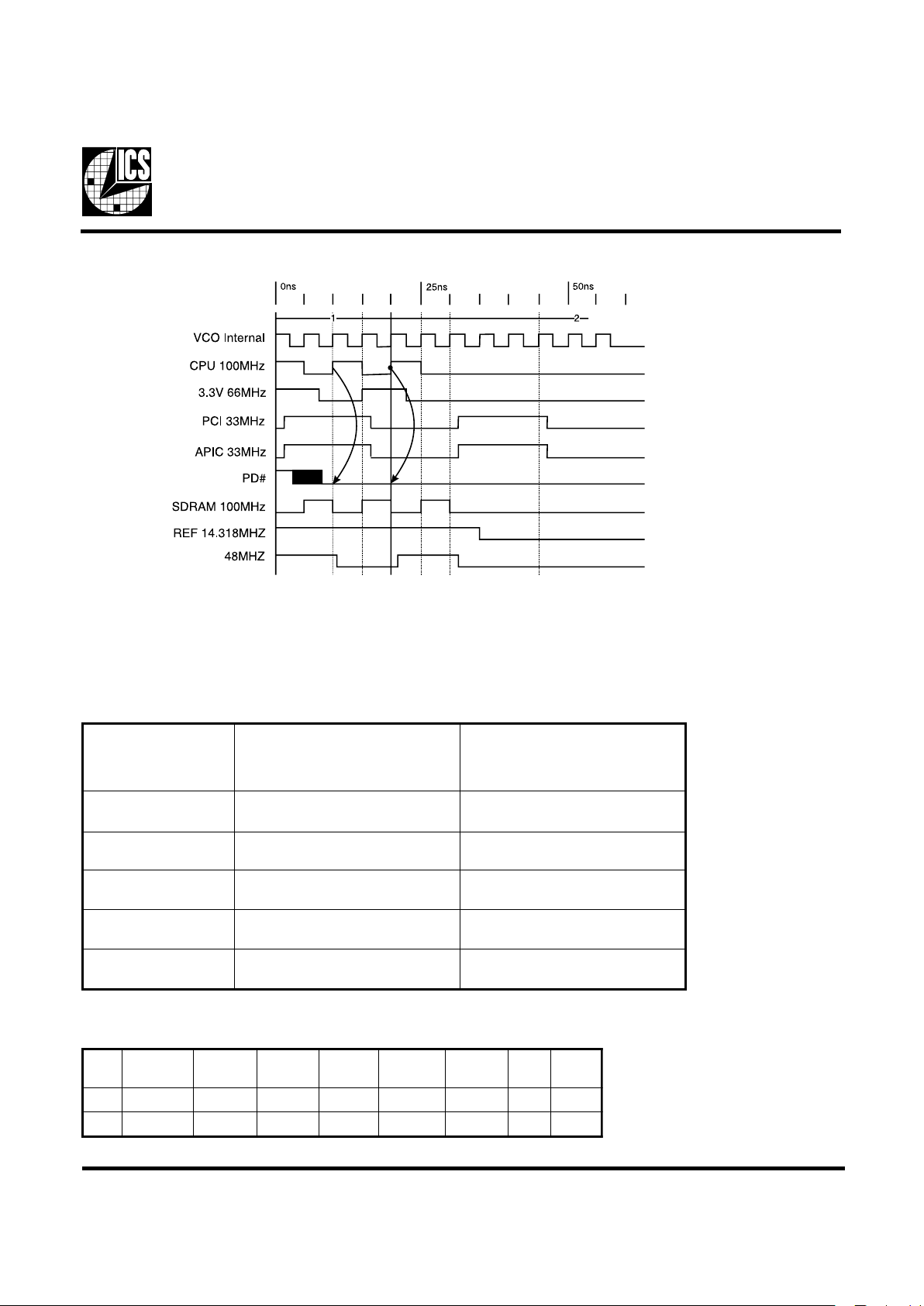
Group Offset Waveforms
Cycle Repeats
0ns
CPU 66MHz
CPU 100MHz
CPU 133MHz
SDRAM 133MHz
SDRAM 100MHz
3.3V 66MHz
PCI 33MHz
IOAPIC 33MHz
REF 14.318MHz
USB 48MHz
10ns 20ns 30ns 40ns

14
ICS9250-29
Fig. 1
Shared Pin Operation Input/Output Pins
The I/O pins designated by (input/output) on the ICS9250-29
serve as dual signal functions to the device. During initial
power-up, they act as input pins. The logic level (voltage) that
is present on these pins at this time is read and stored into a 5bit internal data latch. At the end of Power-On reset, (see AC
characteristics for timing values), the device changes the
mode of operations for these pins to an output function. In this
mode the pins produce the specified buffered clocks to external
loads.
To program (load) the internal configuration register for these
pins, a resistor is connected to either the VDD (logic 1) power
supply or the GND (logic 0) voltage potential. A 10 Kilohm
(10K) resistor is used to provide both the solid CMOS
programming voltage needed during the power-up
programming period and to provide an insignificant load on
the output clock during the subsequent operating period.
Via to
VDD
Clock trace to load
Series Term. Res.
Programming
Header
Via to Gnd
Device
Pad
2K
8.2K
Figure 1 shows a means of implementing this function when
a switch or 2 pin header is used. With no jumper is installed
the pin will be pulled high. With the jumper in place the pin
will be pulled low. If programmability is not necessary, than
only a single resistor is necessary. The programming resistors
should be located close to the series termination resistor to
minimize the current loop area. It is more important to locate
the series termination resistor close to the driver than the
programming resistor.
TRISTATE#/PD# pin description:
The TRISTATE#/PD# pin provides the capability of invoking
Tristate mode during board level testing.
At power up the TRISTATE#/PD# pin defaults to the
TRISTATE# input function to enable the TRESTATE# and
TEST modes.
Approximately 1.5ms to 3ms after power on, the TRISTATE#/
PD# changes to the PD# input function and the TRISTATE#
functionality is disabled (if TRISTATE# is not active).

15
ICS9250-29
ICS reserves the right to make changes in the device data identified in this
publication without further notice. ICS advises its customers to obtain the
latest version of all device data to verify that any information being relied
upon by the customer is current and accurate.
Ordering Information
ICS9250yF-29-T
Designation for tape and reel packaging
Pattern Number (2 or 3 digit number for parts with ROM code patterns)
Package Type
F=SSOP
Revision Designator (will not correlate with datasheet revision)
Device Type (consists of 3 or 4 digit numbers)
Prefix
ICS, AV = Standard Device
Example:
ICS XXXX y F - PPP - T
MIN MAX MIN MAX
A 2.413 2.794 .095 .110
A1 0.203 0.406 .008 .016
b 0.203 0.343 .008 .0135
c 0.127 0.254 .005 .010
D
E 10.033 10.668 .395 .420
E1 7.391 7.595 .291 .299
e 0.635 BA SIC 0.025 BASIC
h 0.381 0.635 .015 .025
L 0.508 1.016 .020 .040
N
α
0° 8° 0° 8°
VARIATIONS
MIN MAX MIN MAX
56 18.288
18.542
.720 .730
JEDEC MO-118
DOC# 10-0034
6/1/00
REV B
N
D mm.
D (inch)
SEE VARIATIONS
SYMBOL
SEE VARIATIONS
SEE VARIATIONS
In Millimeters
COMMON DIMENSIONS
In Inches
COMMON DIMENSIONS
SEE VARIATIONS
 Loading...