

Integrated
Circuit
Systems, Inc.
ICS9250-28
Third party brands and names are the property of their respective owners.
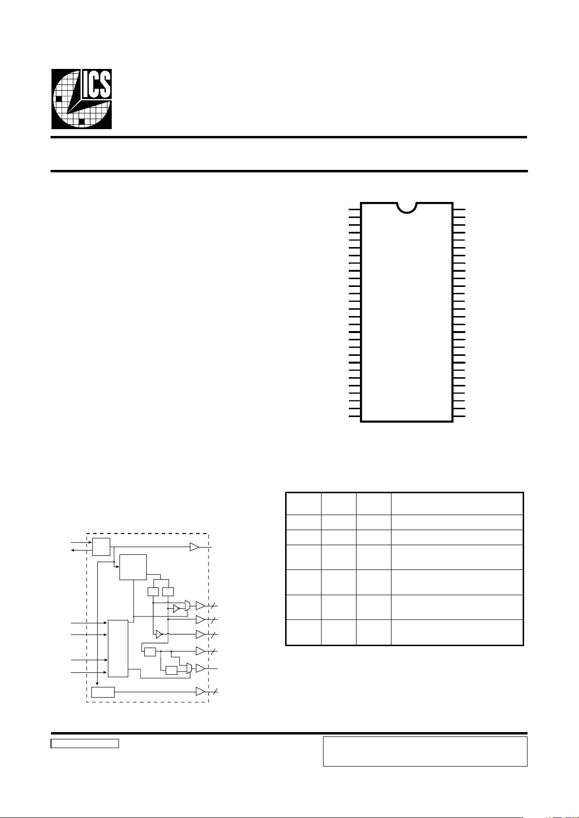
Block Diagram
9250-28 Rev B 10/26/00
Recommended Application:
810/810E and 815 type chipset.
Output Features:
• 2 CPU (2.5V) (up to 133MHz achievable through I
2
C)
• 13 SDRAM (3.3V) (up to 133MHz achievable
through I
2
C)
• 2 PCI (3.3 V) @33.3MHz
• 1 IOAPIC (2.5V) @ 33.3 MHz
• 3 Hublink clocks (3.3 V) @ 66.6 MHz
• 2 (3.3V) @ 48 MHz (Non spread spectrum)
• 1 REF (3.3V) @ 14.318 MHz
Features:
• Supports spread spectrum modulation,
0 to -0.5% down spread.
•I
2
C support for power management
• Efficient power management scheme through PD#
• Uses external 14.138 MHz crystal
• Alternate frequency selections available through I
2
C
control.
Functionality
Pin Configuration
56-Pin 300mil SSOP
* This input has a 50KW pull-down to GND.
IOAPIC
VDDL
GND
*FS1/REF0
VDDREF
X1
X2
GND
VDD3V66
3V66_0
3V66_1
3V66_2
GND
VDDPCI
PCICLK0
PCICLK1
GND
FS0
GND
VDDA
PD#
SCLK
S DATA
GND
VDD48
48MHz_0
48MHz_1
FS2
VDDL
GND
CPUCLK0
CPUCLK1
GND
SDRAM0
SDRAM1
VDDSDR
GND
SDRAM2
SDRAM3
SDRAM4
VDDSDR
GND
SDRAM5
SDRAM6
VDDSDR
GND
SDRAM7
SDRAM8
SDRAM9
VDDSDR
GND
SDRAM10
SDRAM11
VDDSDR
GND
SDRAM12
ICS9250-28
1
2
3
4
5
6
7
8
9
10
11
12
13
14
15
16
17
18
19
20
21
22
23
24
25
26
27
28
56
55
54
53
52
51
50
49
48
47
46
45
44
43
42
41
40
39
38
37
36
35
34
33
32
31
30
29
Frequency Generator & Integrated Buffers for Celeron & PII/III™
2SF0SF1SFnoitcnuF
00X etatsirT
01XtseT
100
zHM66=UPCevitcA
zHM001=MARDS
110
zHM001=UPCevitcA
zHM001=MARDS
101
zHM331=UPCevitcA
zHM331=MARDS
111
zHM331=UPCevitcA
zHM001=MARDS
REF0
CPU66/100/133 [1:0]
3V66 (2:0)
SDRAM (12:0)
PCICLK (1:0)
IOAPIC
PLL2
48MHz (1:0)
X1
X2
XTAL
OSC
Control
Logic
Config
Reg
FS(2:0)
PD#
2
2
3
13
2
/2
/2
/3
/2
PLL1
Spread
Spectrum
SDATA
SCLK
ICS reserves the right to make changes in the device data identified in
this publication without further notice. ICS advises its customers to
obtain the latest version of all device data to verify that any
information being relied upon by the customer is current and accurate.
Power Groups
Analog
VDDREF = X1, X2
VDDA = PLL1
VDD48 = PLL2
Digital
VDD3V66, VDDPCI
VDDSDR, VDDL
2
ICS9250-28
The ICS9250-28 is part of a two chip clock solution for 810/810E and 815 type chipset. Combined with the
ICS9112-17, the ICS9250-28 provides all necessary clock signals for such a system.
Spread spectrum may be enabled through I
2
C programming. Spread spectrum typically reduces EMI by 8dB to 10
dB. This simplifies EMI qualification without resorting to board design iterations or costly shielding. The
ICS9250-28 employs a proprietary closed loop design, which tightly controls the percentage of spreading over
process and temperature variations.
General Description
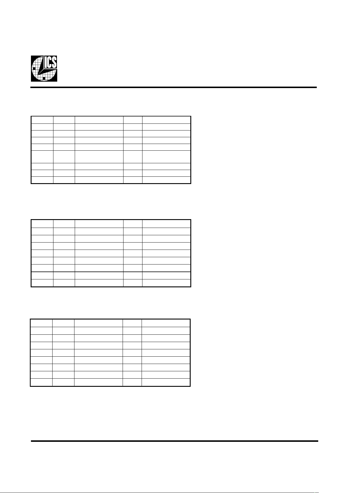
Pin Configuration
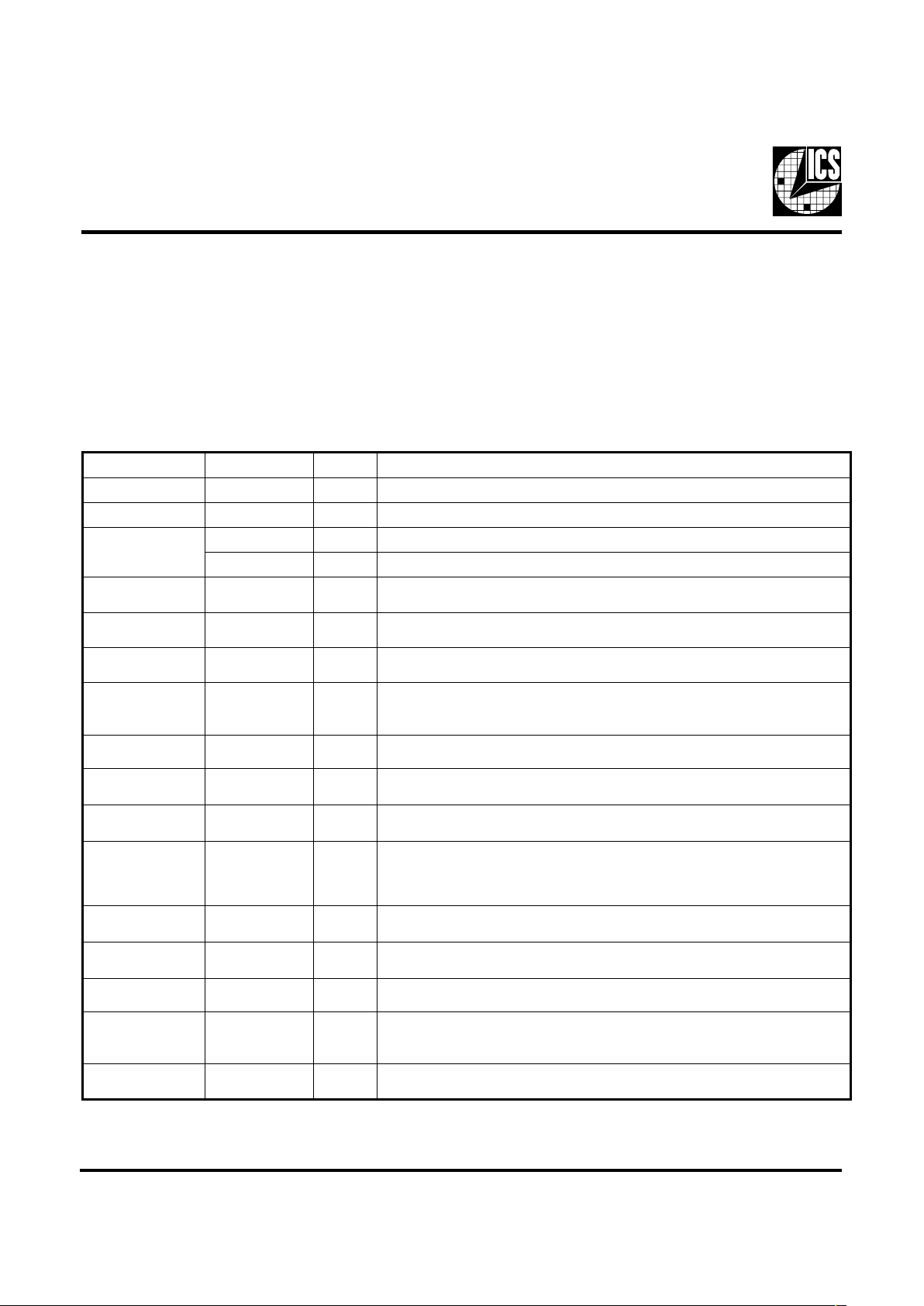
REBMUNNIPEMANNIPEPYTNOITPIRCSED
1CIPAOITUO.zHM3.33tagninnurtuptuokcolcV5.2
65,2LDDVRWPCIPAOI&UPCrofylppusrewopV5.2
4
1SFNIytilanoitcnuftuptuolla,ycneuqerfUPCsenimreteD.niptceleSnoitcnuF
0FERTUO.tuptuokcolcecnereferzHM813.41,V3.3
,52,02,41,9,5
94,44,04,53,13
DDVRWPylppusrewopV3.3
61XNI
kcabdeefdna)Fp33(pacdaollanretnisah,tupnilatsyrC
2Xmorfrotsiser
72XTUO
daollanretnisaH.zHM813.41yllanimon,tuptuolatsyrC
)Fp33(pac
,91,71,31,8,3
,93,43,03,42
55,25,84,34
DNGRWPylppusV3.3rofsnipdnuorG
01,11,21)0:2(66V3TUOBUHrofstuptuokcolczHM66dexiFV3.3
81,82)0,2(SFNI
.ytilanoitcnuftuptuolla,ycneuqerfUPCsenimreteD.sniptceleSnoitcnuF
.3egapnoelbatytilanoitcnuFotreferesaelP
51,61]0:1[KLCICPTUOstuptuokcolcICPV3.3
12#DPNI
otniecivedehtnwodrewopotdesuniptupniwolevitcasuonorhcnysA
dnaOCVehtdnadelbasideraskcolclanretniehT.etatsrewopwola
ebtonlliwnwodrewopehtfoycnetalehT.deppotseralatsyrceht
.sm3nahtretaerg
22KLCSNIIfonipkcolC
2
tnarelotV5yrtiucricC
32ATADSO/IIrofnipataD
2
tnarelotV5yrtiucricC
72,620_zHM84TUO.stuptuokcolczHM84dexiFV3.3
,63,33,23,92
,24,14,83,73
15,05,74,64,54
MARDS
)0:21(
TUO
ffodenrutebnacstuptuoMARDSllA.zHM001gninnurtuptuoV3.3
Ihguorht
2
C
35,45)0:1(KLCUPCTUO
gnidnepedzHM331rozHM001,zHM66.tuptuokcolcsubtsoHV5.2
.snip)0:2(SFno
3
ICS92 50-28
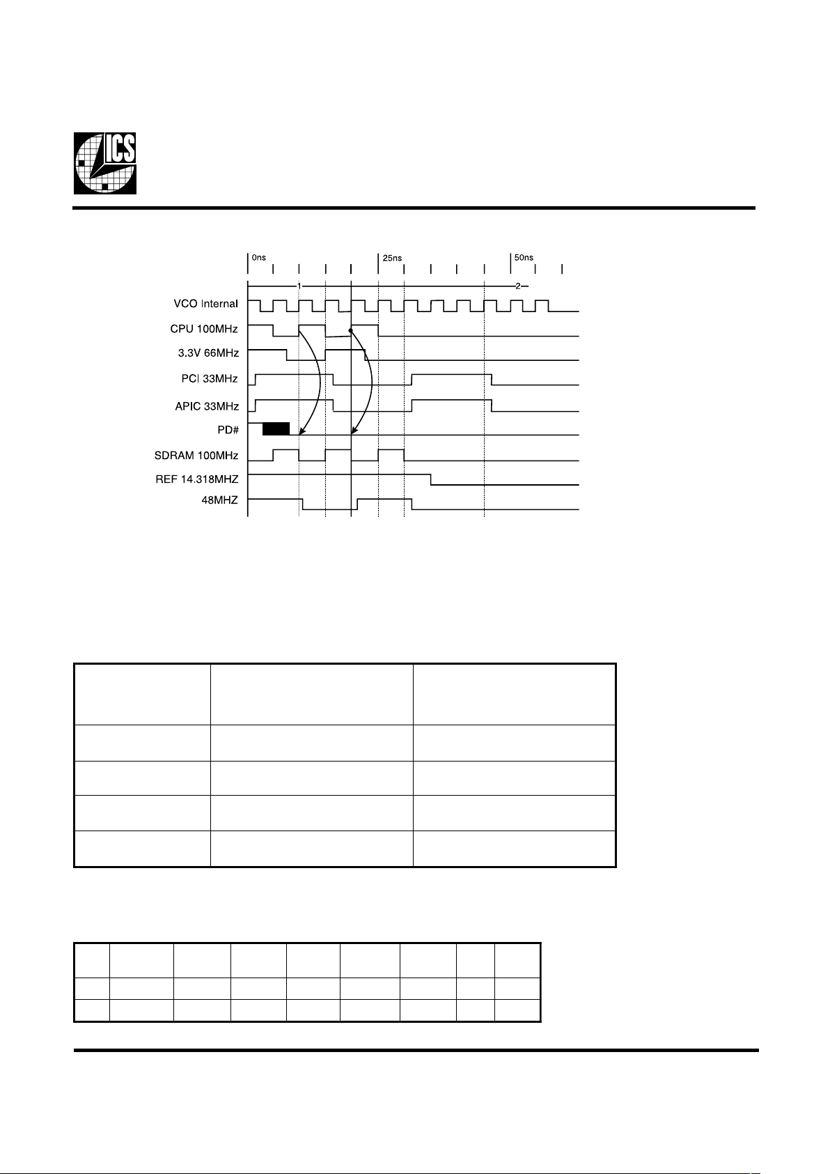
Power Down Waveform
Note
1. After PD# is sampled active (Low) for 2 consective rising edges of CPUCLKs, all
the output clocks are driven Low on their next High to Low tranistiion.
2. Power-up latency <3ms.
3. Waveform shown for 100MHz
Maximum Allowed Current
Clock Enable Configuration
#DPKLCUPCMARDSCIPAOIzHM66KLCICP
,FER
zHM84
csOsOCV
0WOLWOLWOLWOLWOLWOLFFOFFO
1NONONONONONONONO
518
noitidnoC
noitpmusnocylppusV5.2xaM
,sdaolpacetercsidxaM
V526.2=2qddV
DNGro3qddV=stupnicitatsllA
noitpmusnocylppusV5.2xaM
,sdaolpacetercsidxaM
V564.3=2qddV
DNGro3qddV=stupnicitatsllA
edoMnwodrewoP
0=#NWDRWP(
Am01Am01
zHM66evitcAlluF
010=]0:2[SF
Am07Am004
zHM001evitcAlluF
110=]0:2[SF
Am001Am004
zHM331evitcAlluF
111=]0:2[SF
Am031Am054
4
ICS9250-28
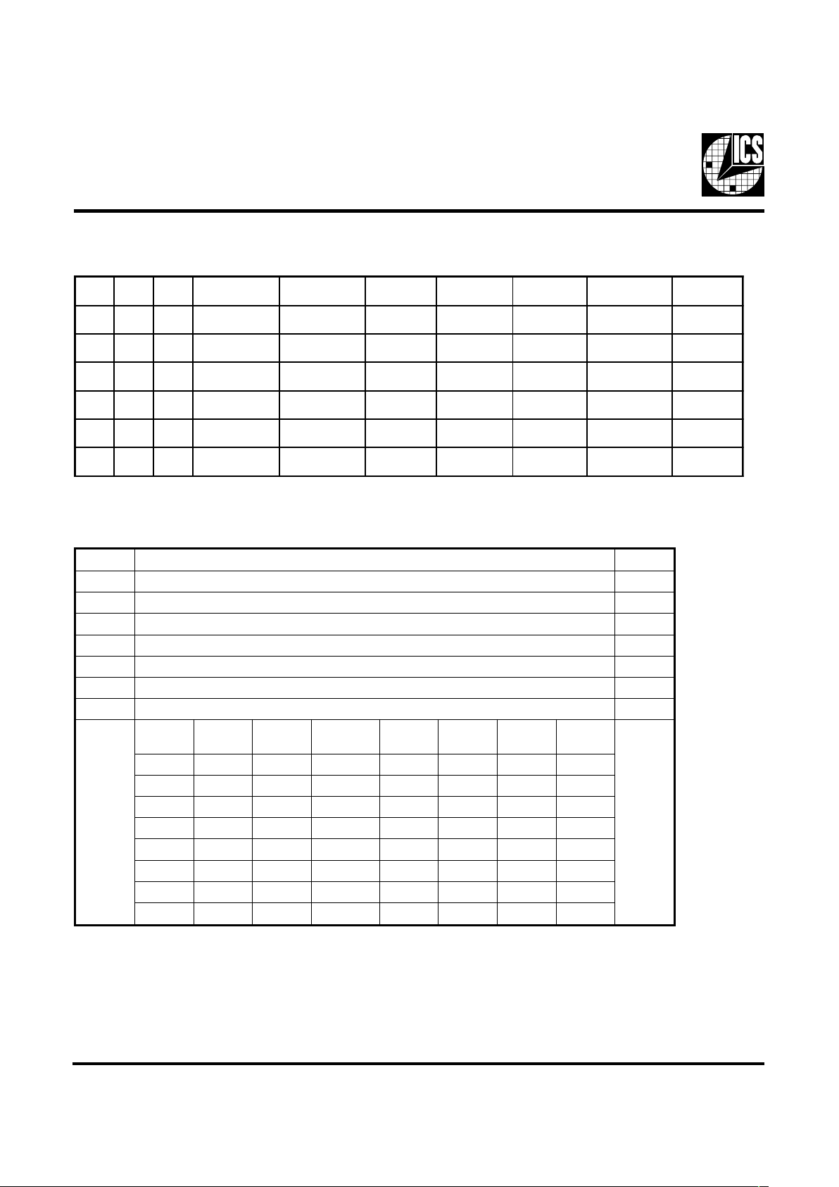
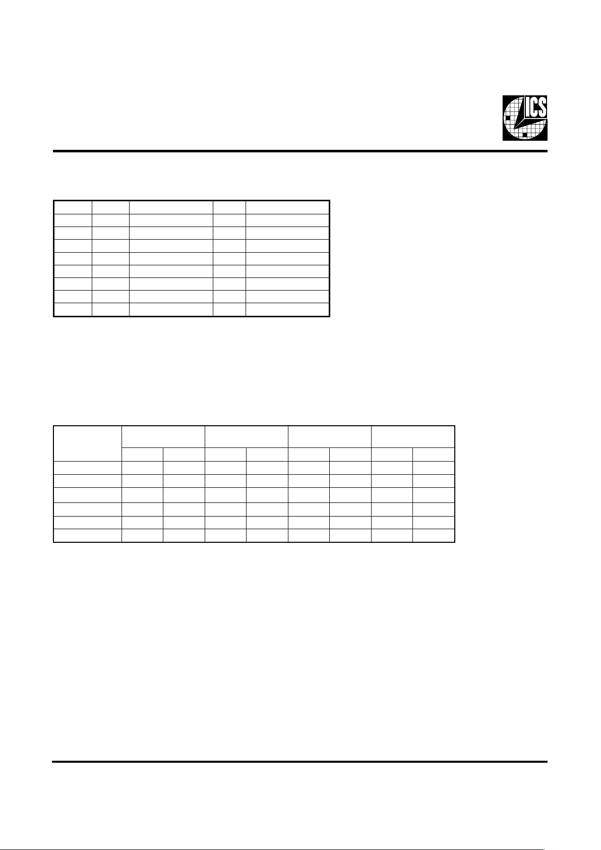
Byte 3: ICS Reserved Functionality and frequency select register (Default as noted in PWD)
2SF0SF1SFUPCMARDS66V3ICPzHM84FERCIPAOI
00X etatsirTetatsirTetatsirTetatsirTetatsirTetatsirTetatsirT
01X 2/KLCT2/KLCT3/KLCT6/KLCT2/KLCTKLCT6/KLCT
100 zHM6.66zHM001zHM6.66zHM3.33zHM84zHM813.41zHM3.33
110 zHM001zHM001zHM6.66zHM3.33zHM84zHM813.41zHM3.33
101 zHM331zHM331zHM6.66zHM3.33zHM84zHM813.41zHM3.33
111 zHM331zHM001zHM6.66zHM3.33zHM84zHM813.41zHM3.33
Truth Table
Note 1: For system operation, the BSEL lines of the CPU will program FS0, FS2 for the appropriate CPU speed, always
with SDRAM = 100MHz. After BIOS verifies the SDRAM is PC133 speed, then bit 0 can be written from the
default 0 to 1 to change the SDRAM output frequency from 100MHz to 133MHz. This will only change if the
CPU is at the 133MHz FSB speed as shown in this table. The CPU, 3V66, PCI, and IOAPIC clocks will be glitch
free during this transition, and only SDRAM will change.
Note 2: "ICS RESERVED BITS" must be writtern as "0".
Note3: Undefined bits can be written either as "1 or 0"
tiBnoitpitcseDDWP
7tiB)2etoN(tibdevreseRSCI 0
6tiB)2etoN(tibdevreseRSCI 0
5tiB)2etoN(tibdevreseRSCI 0
4tiB)2etoN(tibdevreseRSCI 0
3tiB)2etoN(tibdevreseRSCI 0
2tiB)3etoN(tibdenifednU X
1tiB)3etoN(tibdenifednU X
0tiB
0tiB0SF1SF
KLCUPC
zHM
MARDS
zHM
66V3
zHM
KLCICP
zHM
CIPAOI
zHM
0
1etoN
000 66.660.00166.6633.3333.33
010 0.0010.00166.6633.3333.33
001 23.33123.33166.6633.3333.33
011 23.3310.00166.6633.3333.33
100 66.660.00166.6633.3333.33
110 0.0010.00166.6633.3333.33
101 23.33123.33166.6633.3333.33
111 23.33123.33166.6633.3333.33
5
ICS92 50-28
Byte 0: Control Register
(1 = enable, 0 = disable)
Byte 1: Control Register
(1 = enable, 0 = disable)
tiB#niPemaNDWPnoitpircseD
7tiB- DIdevreseR0)evitcanI/evitcA(
6tiB- DIdevreseR0)evitcanI/evitcA(
5tiB- DIdevreseR0)evitcanI/evitcA(
4tiB- DIdevreseR1)evitcanI/evitcA(
3tiB-
murtcepSdaerpS
)ffO=0/nO=1(
1)evitcanI/evitcA(
2tiB721zHM841)evitcanI/evitcA(
1tiB620zHM841)evitcanI/evitcA(
0tiB- DIdevreseR0)evitcanI/evitcA(
tiB#niPemaNDWPnoitpircseD
7tiB837MARDS1)evitcanI/evitcA(
6tiB146MARDS1)evitcanI/evitcA(
5tiB245MARDS1)evitcanI/evitcA(
4tiB544MARDS1)evitcanI/evitcA(
3tiB643MARDS1)evitcanI/evitcA(
2tiB742MARDS1)evitcanI/evitcA(
1tiB051MARDS1)evitcanI/evitcA(
0tiB150MARDS1)evitcanI/evitcA(
Note: Reserved ID bits must be written as "0"
Byte 2: Control Register
(1 = enable, 0 = disable)
Notes:
1. Inactive means outputs are held LOW and are disabled from switching. These outputs are designed to be
configured at power-on and are not expected to be configured during the normal modes of operation.
2. PWD = Power on Default
3. Undefined bit can be wirtten with either a "1" or "0".
tiB#niPemaNDWPnoitpircseD
7tiB21)PGA(2-66V31)evitcanI/evitcA(
6tiB9221MARDS1)evitcanI/evitcA(
5tiB2311MARDS1)evitcanI/evitcA(
4tiB3301MARDS1)evitcanI/evitcA(
3tiB639MARDS1)evitcanI/evitcA(
2tiB738MARDS1)evitcanI/evitcA(
1tiB611KLCICP1)evitcanI/evitcA(
0tiB- devreseR0)evitcanI/evitcA(
6
ICS9250-28
Group Timing Relationship Table
1
Byte 4: Reserved Register
(1 = enable, 0 = disable)
tiB#niPemaNDWPnoitpircseD
7tiB- devreseR0)evitcanI/evitcA(
6tiB- devreseR0)evitcanI/evitcA(
5tiB- devreseR0)evitcanI/evitcA(
4tiB- devreseR0)evitcanI/evitcA(
3tiB- devreseR0)evitcanI/evitcA(
2tiB- devreseR0)evitcanI/evitcA(
1tiB- devreseR0)evitcanI/evitcA(
0tiB- devreseR0)evitcanI/evitcA(
Notes:
1. Inactive means outputs are held LOW and are disabled from switching. These outputs are designed to be
configured at power-on and are not expected to be configured during the normal modes of operation.
2. PWD = Power on Default
puorGzHM66UPC
zHM001MARDS
zHM001UPC
zHM001MARDS
zHM331UPC
zHM001MARDS
zHM331UPC
zHM331MARDS
tesffOecnareloTtesffOecnareloTtesffOecnareloTtesffOecnareloT
MARDSotUPCsn5.2-sp005sn0.5sp005sn0.0sp005sn57.3sp005
66V3otUPCsn5.7sp005sn0.5sp005sn0.0sp005sn0.0sp005
66V3otMARDSsn0.0sp005sn0.0sp005sn0.0sp005sn57.3-sp005
ICPot66V3sn5.3-5.1sp005sn5.3-5.1sp005sn5.3-5.1sp005sn5.3-5.1sp005
ICPotICPsn0.0sp005sn0.0sp005sp005sn0.1sn0.0sp005
TOD&BSUhcnysAA/NhcnysAA/NhcnysAA/NhcnysAA/N

7
ICS92 50-28
Absolute Maximum Ratings
Core Supply Voltage . . . . . . . . . . . . . . . . . . . . . . . 4.6 V
I/O Supply Voltage . . . . . . . . . . . . . . . . . . . . . . . . 3.6V
Logic Inputs . . . . . . . . . . . . . . . . . . . . . . . . . . . . . . GND –0.5 V to V
DD
+0.5 V
Ambient Operating Temperature. . . . . . . . . . . . . 0°C to +70°C
Maximum Case Operating Temperature . . . . . . +135°C
Storage Temperature . . . . . . . . . . . . . . . . . . . . . . . –65°C to +150°C
Stresses above those listed under Absolute Maximum Ratings may cause permanent damage to the device. These ratings are
stress specifications only and functional operation of the device at these or any other conditions above those listed in the
operational sections of the specifications is not implied. Exposure to absolute maximum rating conditions for extended
periods may affect product reliability.
Electrical Characteristics - Input/Supply/Common Output Parameters
TA = 0 - 70C; Supply Voltage VDD = 3.3 V +/-5%, V
DDL
= 2.5 V +/-5% (unless otherwise stated)
PARAMETER SYMBOL CONDITIONS MIN TYP MAX UNITS
Input High Voltage V
I
H
2V
DD
+0.3 V
Input Low Voltage V
I
L
VSS-0.3 0.8 V
Input High Current I
I
H
V
I
N
= V
DD
-5 5
µA
I
I
L1
V
I
N
= 0 V; Inputs with no pull-up resistors -5
I
IL2
VIN = 0 V; Inputs with pull-up resistors
-200
C
L
= 0 pF; @ 66/100 MHz 138 200
C
L
= 0 pF; @ 100/100 MHz 126 200
C
L
= 0 pF; @ 133/133 MHz 172 200
C
L
= 0 pF; @ 133/100 MHz 141 200
C
L
= Max loads; @ 66/10 0 MHz 339 400
C
L
= Max loads; @ 100/100 MHz 328 400
C
L
= Max loads; @ 133/133 MHz 383 450
C
L
= Max loads; @ 133/100 MHz 340 400
C
L
= 0 pF; @ 66/100 MHz 9 15
C
L
= 0 pF; @ 100/100 MHz 11 18
C
L
= 0 pF; @ 133/133 MHz 13 20
C
L
= 0 pF; @ 133/100 MHz 13 20
C
L
= Max loads; @ 66/100 MHz 13 35
C
L
= Max loads; @ 100/100 MHz 23 60
C
L
= Max loads; @ 133/133 MHz 29 60
C
L
= Max loads; @ 133/100 MHz 30 60
I
DD3.3PD
CL = Max loads
251 400
I
DD.25PD
Input address VDD or GND
<1 10
Input Frequency F
i
VDD = 3.3 V 12 14.318 16 MHz
Transition time
1
T
trans
To 1st crossing of target freque ncy 3 ms
Settling time
1
T
s
From 1st crossing to 1% target frequency 3 ms
Clk Stabilization
1
T
STAB
From VDD = 3.3 V to 1% target frequency 3 ms
t
PZH,tPZL
Output enable delay (all outputs) 1 10 ns
t
PHZ,tPLZ
Output disable delay (all output s) 1 10 ns
1
Guaranteed by design, not 100% tested in production.
Delay
1
mA
mA
I
DD2.5OP
µA
Powerdown Current
Operating Supply
Current
Input Low Current
µA
mA
mA
I
DD3.3OP

8
ICS9250-28
Electrical Characteristics - CPU
TA = 0 - 70C; V
DDL
= 2.5 V +/-5%; CL = 10-20 pF (unless otherwise specified)
PARAMETER SYMBOL CONDITIONS MIN TYP MAX UNITS
Output Impedance R
DSP2B
1
VO = VDD*(0.5) 13.5 16 45 Ω
Output Impedance R
DSN2B
1
VO = VDD*(0.5) 13.5 21 45 Ω
Output High Volt age V
OH2B
IOH = -1 mA 2 V
Output Low Voltage V
OL2B
IOL = 1 mA 0.4 V
V
OH @ MIN
= 1.0 V -27 -68
V
OH @ MAX
= 2.375 V -9 -27
V
OL @ MIN
= 1.2 V 27 54
V
OL @ MAX
= 0.3 V 11 30
Rise Time
1
t
r2B
VOL = 0.4 V, VOH = 2.0 V 0.4 1.1 1.6 ns
Fall Time
1
t
f
2B
VOH = 2.0 V, VOL = 0.4 V 0.4 1.1 1.6 ns
Duty Cycle
1
d
t2B
VT = 1.25 V 45 49 55 %
Skew window
1
t
sk2B
VT = 1.25 V 45 175 ps
Jitter, Cycle-to-cycle
1
t
jcyc-cyc2B
VT = 1.25 V
135 250 ps
1
Guaranteed by design, not 100% tested in production.
mA
mA
Output High Current
Output Low Current
I
OH2B
I
OL2B
Electrical Characteristics - 3V66
TA = 0 - 70C; VDD = 3.3 V +/-5%; CL = 10-20 pF (unless otherwise specified)
PARAMETER SYMBOL CONDITIONS MIN TYP MAX UNITS
Output Impedance R
DSP1B
1
VO = VDD*(0.5) 12 14 55 Ω
Output Impedance R
DSN1B
1
VO = VDD*(0.5) 12 14.5 55 Ω
Output High Volt age V
OH1
IOH = -1 mA 2.4 V
Output Low Voltage V
OL1
IOL = 1 mA 0.55 V
V
OH @ MIN
= 1.0 V -33 -108
V
OH @ MAX
= 3.135 V -9 -33
V
OL @ MIN
= 1.95 V 30 95
V
OL @ MAX
= 0.4 V 29 38
Rise Time
1
t
r1
VOL = 0.4 V, VOH = 2.4 V 0.4 1.2 1.6 ns
Fall Time
1
t
f
1
VOH = 2.4 V, VOL = 0.4 V 0.4 1.2 1.6 ns
Duty Cycle
1
d
t1
VT = 1.5 V 45 49 55 %
Skew window
1
t
sk1
VT = 1.5 V 135 175 ps
Jitter, Cycle-to-cycle
1
t
jcyc-cyc1
VT = 1.5 V
175 500 ps
1
Guaranteed by design, not 100% tested in production.
Output High Current
Output Low Current
mA
mA
I
OH1
I
OL1

9
ICS92 50-28
Electrical Characteristics - IOAPIC
TA = 0 - 70C; V
DDL
= 2.5 V +/-5%; CL = 10-20 pF (unless otherwise specified)
PARAMETER SYMBOL CONDITIONS MIN TYP MAX UNITS
Output Impedance R
DSP4B
1
VO = VDD*(0.5) 9 16 30 Ω
Output Impedance R
DSN4B
1
VO = VDD*(0.5) 9 20 30 Ω
Output High Volt age V
OH4B
IOH = -1 mA 2 V
Output Low Voltage V
OL4B
IOL = 1 mA 0.4 V
V
OH @ MIN
= 1.0 V -27 -68
V
OH @ MAX
= 2.375 V -9 -27
V
OL @ MIN
= 1.2 V 27 54
V
OL @ MAX
= 0.3 V 11 30
Rise Time
1
t
r4B
VOL = 0.4 V, VOH = 2.0 V 0.4 1.1 1.6 ns
Fall Time
1
t
f
4B
VOH = 2.0 V, VOL = 0.4 V 0.4 1.1 1.6 ns
Duty Cycle
1
d
t4B
VT = 1.25 V 45 49 55 %
Jitter, Cycle-to-cycle
1
t
jcyc-cyc4B
VT = 1.25 V
180 500 ps
1
Guaranteed by design, not 100% tested in production.
Output High Current
I
OH4B
mA
Output Low Current
I
OL4B
mA
Electrical Characteristics - SDRAM
TA = 0 - 70C; VDD = 3.3 V +/-5%; CL = 20-30 pF (unless otherwise specified)
PARAMETER SYMBOL CONDITIONS MIN TYP MAX UNITS
Output Impedance R
DSP3B
1
VO = VDD*(0.5) 10 12 24 Ω
Output Impedance R
DSN3B
1
VO = VDD*(0.5) 10 15 24 Ω
Output High Volt age V
OH3
IOH = -1 mA 2.4 V
Output Low Voltage V
OL3
IOL = 1 mA 0.4 V
V
OH @ MIN
= 2.0 V -54 -92
V
OH @ MAX
= 3.135 V -16 -46
V
OL @ MIN
= 1.0 V 54 68
V
OL @ MAX
= 0.4 V 29 53
Rise Time
1
t
r3
VOL = 0.4 V, VOH = 2.4 V 0.4 1 1.6 ns
Fall Time
1
t
f
3
VOH = 2.4 V, VOL = 0.4 V 0.4 1.5 1.6 ns
Duty Cycle
1
d
t3
VT = 1.5 V 45 52 55 %
Skew window
1
t
sk3
VT = 1.5 V 120 250 ps
Jitter, Cycle-to-cycle
1
t
jcyc-cyc3
VT = 1.5 V
135 250
ps
1
Guaranteed by design, not 100% tested in production.
mA
mA
Output High Current
Output Low Current
I
OH3
I
OL3

10
ICS9250-28
Electrical Characteristics - PCI
TA = 0 - 70C; VDD = 3.3 V +/-5%; CL = 10-30 pF (unless otherwise specified)
PARAMETER SYMBOL CONDITIONS MIN TYP MAX UNITS
Output Impedance R
DSP1B
1
VO = VDD*(0.5) 12 15 55 Ω
Output Impedance R
DSN1B
1
VO = VDD*(0.5) 12 15 55 Ω
Output High Volt age V
OH1
IOH = -1 mA 2.4 V
Output Low Voltage V
OL1
IOL = 1 mA 0.55 V
V
OH @ MIN
= 1.0 V -33 -106
V
OH @ MAX
= 3.135 V -14 -33
V
OL @ MIN
= 1.95 V 30 94
V
OL @ MAX
= 0.4 V 29 38
Rise Time
1
t
r1
VOL = 0.4 V, VOH = 2.4 V 0.4 1.3 2 ns
Fall Time
1
t
f
1
VOH = 2.4 V, VOL = 0.4 V 0.4 1.4 2 ns
Duty Cycle
1
d
t1
VT = 1.5 V 45 51 55 %
Skew window
1
t
sk1
VT = 1.5 V 20 500 ps
Jitter, Cycle-to-cycle
1
t
jcyc-cyc1
VT = 1.5 V
175 500 ps
1
Guaranteed by design, not 100% tested in production.
Output High Current
I
OH1
mA
Output Low Current
I
OL1
mA
Electrical Characteristics - REF, 48MHz_0 (Pin 26)
TA = 0 - 70C; VDD = 3.3 V +/-5%; CL = 10-20 pF (unless otherwise specified)
PARAMETER SYMBOL CONDITIONS MIN TYP MAX UNITS
Output Impedance R
DSP5B
1
VO = VDD*(0.5) 20 29 60 Ω
Output Impedance R
DSN5B
1
VO = VDD*(0.5) 20 27 60 Ω
Output High Volt age V
OH15
IOH = -1 mA 2.4 V
Output Low Voltage V
OL5
IOL = 1 mA 0.55 V
V
OH @ MIN
= 1.0 V -29 -54
V
OH @ MAX
= 3.135 V -11 -23
V
OL @ MIN
= 1.95 V 29 54
V
OL @ MAX
= 0.4 V 16 27
Rise Time
1
t
r5
VOL = 0.4 V, VOH = 2.4 V 0.4 1.3 4 ns
Fall Time
1
t
f
5
VOH = 2.4 V, VOL = 0.4 V 0.4 1.6 4 ns
Duty Cycle
1
d
t5
VT = 1.5 V 45 53 55 %
Jitter, Cycle-to-cycle
1
t
jcyc-cyc5
VT = 1.5 V, Fixed clocks 160 500 ps
Jitter, Cycle-to-cycle
1
t
jcyc-cyc5
VT = 1.5 V, Ref clocks
420 1000 ps
1
Guaranteed by design, not 100% tested in production.
Output High Current
I
OH5
mA
Output Low Current
I
OL5
mA

11
ICS92 50-28
Electrical Characteristics - 48MHz_1 (Pin 27)
TA = 0 - 70C; VDD = 3.3 V +/-5%; CL = 10-15 pF (unless otherwise specified)
PARAMETER SYMBOL CONDITIONS MIN TYP MAX UNITS
Output Impedance R
DSP3B
1
VO = VDD*(0.5) 10 15 24 Ω
Output Impedance R
DSN3B
1
VO = VDD*(0.5) 10 15 24 Ω
Output High Volt age V
OH3
IOH = -1 mA 2.4 V
Output Low Voltage V
OL3
IOL = 1 mA 0.55 V
V
OH @ MIN
= 2.0 V -54 -82
V
OH @ MAX
= 3.135 V -20 -46
V
OL @ MIN
= 1.0 V 54 95
V
OL @ MAX
= 0.4 V 28 53
Rise Time
1
t
r3
VOL = 0.4 V, VOH = 2.4 V 0.4 1.1 1.6 ns
Fall Time
1
t
f
3
VOH = 2.4 V, VOL = 0.4 V 0.4 1.3 1.6 ns
Duty Cycle
1
d
t3
VT = 1.5 V 45 53 55 %
Jitter, Cycle-to-cycle
1
t
jcyc-cyc3B
VT = 1.5 V
145 500 ps
1
Guaranteed by design, not 100% tested in production.
Output High Current
I
OH3
mA
Output Low Current
I
OL3
mA

12
ICS9250-28
Group Skews (CPU 66 MHz , SDRAM 100MHz)
TA = 0 - 70º C; VDD = 3.3 V +/-5%, V
DDL
= 2.5 V +/-5%
CPU & IOAPIC load (lumped) = 20 pF; PCI, SDRAM, 3V66 load (lumped) = 30 pF
R
efer to Group Offset Waveforms diagram for definition of transition edges.
PARAMETER SYMBOL CONDITIONS MIN TYP MAX UNITS
CPU to SDRAM Skew
1
T
sk1 CPU-SDRAM
-3 -2.7 -2 ns
Skew Window
1
T
w
1 CPU-SDRAM
0 165 500 ps
CPU to 3V66 Skew
1
T
sk1 CPU-3V66
77.68ns
Skew Window
1
T
w
1 CPU-3V66
0 105 500 ps
SDRAM to 3V66 Skew
1
T
sk1 SDRAM-3V66
-500 180 500 ps
Skew Window
1
T
w
1 SDRAM-3V66
0 210 500 ps
3V66 to PCI Skew
1
T
sk1 3V66-PCI
1.5 2.1 3.5 ns
Skew Window
1
T
w
1 3V66-PCI
0 90 500 ps
I
OAPIC to PCI Skew
1
T
sk1 IOAPIC-PCI
-1 -0.1 1 ns
Skew Window
1
T
w1 IOAPIC-PCI
001ns
1
Guaranteed by design, not 100% tested in production.
Group Skews (CPU 100 MHz , SDRAM 100MHz)
TA = 0 - 70º C; VDD = 3.3 V +/-5%, V
DDL
= 2.5 V +/-5%
CPU & IOAPIC load (lumped) = 20 pF; PCI, SDRAM, 3V66 load (lumped) = 30 pF
R
efer to Group Offset Waveforms diagram for definition of transition edges.
PARAMETER SYMBOL CONDITIONS MIN TYP MAX UNITS
CPU to SDRAM Skew
1
T
sk2 CPU-SDRAM
4.5 4.9 5.5 ns
Skew Window
1
T
w
2 CPU-SDRAM
0 180 500 ps
CPU to 3V66 Skew
1
T
sk2 CPU-3V66
4.5 5 5.5 ns
Skew Window
1
T
w
2 CPU-3V66
0 100 500 ps
SDRAM to 3V66 Skew
1
T
sk2 SDRAM-3V66
-500 175 500 ps
Skew Window
1
T
w
2 SDRAM-3V66
0 200 500 ps
3V66 to PCI Skew
1
T
sk2 3V66-PCI
1.5 2.1 3.5 ns
Skew Window
1
T
w
2 3V66-PCI
0 90 500 ps
I
OAPIC to PCI Skew
1
T
sk2 IOAPIC-PCI
-1 -0.1 1 ns
Skew Window
1
T
w2 IOAPIC-PCI
001ns
1
Guaranteed by design, not 100% tested in production.
CPU @ 1.25 V, 3V66 @ 1.5 V
SDRAM, 3V66 @ 1.5 V
3V66, PCI @ 1.5 V
IOAPIC @ 1.25 V, PCI @ 1.5 V
CPU @ 1.25 V, SDRAM @ 1.5 V
CPU @ 1.25 V, SDRAM @ 1.5 V
CPU @ 1.25 V, 3V66 @ 1.5 V
SDRAM, 3V66 @ 1.5 V
3V66, PCI @ 1.5 V
IOAPIC @ 1.25 V, PCI @ 1.5 V

13
ICS92 50-28
Group Skews (CPU 133 MHz , SDRAM 133MHz)
TA = 0 - 70º C; VDD = 3.3 V +/-5%, V
DDL
= 2.5 V +/-5%
CPU & IOAPIC load (lumped) = 20 pF; PCI, SDRAM, 3V66 load (lumped) = 30 pF
R
efer to Group Offset Waveforms diagram for definition of transition edges.
PARAMETER SYMBOL CONDITIONS MIN TYP MAX UNITS
CPU to SDRAM Skew
1
T
sk3 CPU-SDRAM
3.25 3.45 4.25 ns
Skew Window
1
T
w
3 CPU-SDRAM
0 155 500 ps
CPU to 3V66 Skew
1
T
sk3 CPU-3V66
-500 120 500 ps
Skew Window
1
T
w
3 CPU-3V66
0 120 500 ps
SDRAM to 3V66 Skew
1
T
sk3 SDRAM-3V66
-3.25 -3.08 -4.25 ps
Skew Window
1
T
w
3 SDRAM-3V66
0 175 500 ps
3V66 to PCI Skew
1
T
sk3 3V66-PCI
1.5 2.2 3.5 ns
Skew Window
1
T
w
3 3V66-PCI
0 80 500 ps
I
OAPIC to PCI Skew
1
T
sk3 IOAPIC-PCI
-1 -0.1 1 ns
Skew Window
1
T
w3 IOAPIC-PCI
001ns
1
Guaranteed by design, not 100% tested in production.
Group Skews (CPU133 MHz , SDRAM 100MHz)
TA = 0 - 70º C; VDD = 3.3 V +/-5%, V
DDL
= 2.5 V +/-5%
CPU & IOAPIC load (lumped) = 20 pF; PCI, SDRAM, 3V66 load (lumped) = 30 pF
R
efer to Group Offset Waveforms diagram for definition of transition edges.
PARAMETER SYMBOL CONDITIONS MIN TYP MAX UNITS
CPU to SDRAM Skew
1
T
sk3 CPU-SDRAM
CPU @ 1.25 V, SDRAM @ 1. 5 V -500 -15 500 ps
Skew Window
1
T
w
3 CPU-SDRAM
0 165 500 ps
CPU to 3V66 Skew
1
T
sk3 CPU-3V66
CPU @ 1.25 V, 3V66 @ 1.5 V -500 165 500 ps
Skew Window
1
T
w
3 CPU-3V66
0 105 500 ps
SDRAM to 3V66 Skew
1
T
sk3 SDRAM-3V66
SDRAM, 3V66 @ 1.5 V -500 185 500 ps
Skew Window
1
T
w
3 SDRAM-3V66
0 185 500 ps
3V66 to PCI Skew
1
T
sk3 3V66-PCI
3V66, PCI @ 1.5 V 1.5 2.2 3.5 ns
Skew Window
1
T
w
3 3V66-PCI
0 60 500 ps
I
OAPIC to PCI Skew
1
T
sk3 IOAPIC-PCI
IOAPIC @ 1.25 V, PCI @ 1.5 V -1 -0.1 1 ns
Skew Window
1
T
w3 IOAPIC-PCI
001ns
1
Guaranteed by design, not 100% tested in production.
CPU @ 1.25 V, 3V66 @ 1.5 V
SDRAM, 3V66 @ 1.5 V
3V66, PCI @ 1.5 V
IOAPIC @ 1.25 V, PCI @ 1.5 V
CPU @ 1.25 V, SDRAM @ 1.5 V

14
ICS9250-28
Group Offset Waveforms
Cycle Repeats
0ns
CPU 66MHz
CPU 100MHz
CPU 133MHz
SDRAM 133MHz
SDRAM 100MHz
3V66MHz
PCI 33MHz
APIC 33MHz
REF 14.318MHz
USB 48MHz
10ns 20ns 30ns 40ns

15
ICS92 50-28
1. The ICS clock generator is a slave/receiver, I2C component. It can read back the data stored in the latches for
verification. Read-Back will support Intel PIIX4 "Block-Read" protocol.
2. The data transfer rate supported by this clock generator is 100K bits/sec or less (standard mode)
3. The input is operating at 3.3V logic levels.
4. The data byte format is 8 bit bytes.
5. To simplify the clock generator I
2
C interface, the protocol is set to use only "Block-Writes" from the controller. The
bytes must be accessed in sequential order from lowest to highest byte with the ability to stop after any complete byte
has been transferred. The Command code and Byte count shown above must be sent, but the data is ignored for those
two bytes. The data is loaded until a Stop sequence is issued.
6. At power-on, all registers are set to a default condition, as shown.
General I2C serial interface information
The information in this section assumes familiarity with I2C programming.
For more information, contact ICS for an I
2
C programming application note.
How to Write:
Controller (host) sends a start bit.
Controller (host) sends the write address D2
(H)
ICS clock will acknowledge
Controller (host) sends a dummy command code
ICS clock will acknowledge
Controller (host) sends a dummy byte count
ICS clock will acknowledge
Controller (host) starts sending first byte (Byte 0)
through byte 5
ICS clock will acknowledge each byte one at a time.
Controller (host) sends a Stop bit
How to Read:
Controller (host) will send start bit.
Controller (host) sends the read address D3
(H)
ICS clock will acknowledge
ICS clock will send the byte count
Controller (host) acknowledges
ICS clock sends first byte (Byte 0) through byte 5
Controller (host) will need to acknowledge each byte
Controller (host) will send a stop bit
Notes:
Controller (Host) ICS (Slave/Receiver)
Start Bit
Address
D3
(H)
ACK
Byte Count
ACK
Byte 0
ACK
Byte 1
ACK
Byte 2
ACK
Byte 3
ACK
Byte 4
ACK
Byte 5
ACK
Stop Bit
How to Read:
Controller (Host) ICS (Slave/Receiver)
Start Bit
Address
D2
(H)
ACK
Dummy Command Code
ACK
Dummy Byte Count
ACK
Byte 0
ACK
Byte 1
ACK
Byte 2
ACK
Byte 3
ACK
Byte 4
ACK
Byte 5
ACK
Stop Bit
How to Write:

16
ICS9250-28
Connections to VDD:
General Layout Precautions:
1) Use a ground plane on the top routing
layer of the PCB in all areas not used
by traces.
2) Make all power traces and ground
traces as wide as the via pad for lower
inductance.
Notes:
1 All clock outputs should have
provisions for a 15pf capacitor
between the clock output and series
terminating resistor. Not shown in
all places to improve readability of
diagram.
2 Optional crystal load capacitors are
recommended. They should be
included in the layout but not
inserted unless needed.
Component Values:
C1 : Crystal load values determined by user
C2 : 22µF/20V/D case/Tantalum
AVX TAJD226M020R
C3 : 15pF capacitor
FB = Fair-Rite products 2512066017X1
All unmarked capacitors are 0.01µF ceramic
3.3V Power Route
Ground
2.5V Power Route
C1
C1
2
C3
1
Clock Load
Ferrite
Bead
VDD
C2
22µF/20V
Tantalum
56
55
54
53
52
51
50
49
48
47
46
45
44
43
42
41
40
39
38
37
36
35
34
33
32
31
30
29
1
2
3
4
5
6
7
8
Ferrite
Bead
VDD
C2
22µF/20V
Tantalum
1
2
3
4
5
6
7
8
9
10
11
12
13
14
15
16
17
18
19
20
21
22
23
24
25
26
27
28

17
ICS92 50-28
ICS reserves the right to make changes in the device data identified in
this publication without further notice. ICS advises its customers to
obtain the latest version of all device data to verify that any
information being relied upon by the customer is current and accurate.
Ordering Information
ICS9250yF-28-T
Designation for tape and reel packaging
Pattern Number (2 or 3 digit number for parts with ROM code patterns)
Package Type
F=SSOP
Revision Designator (will not correlate with datasheet revision)
Device Type (consists of 3 or 4 digit numbers)
Prefix
ICS, AV = Standard Device
Example:
ICS XXXX y F - PPP - T
MIN MAX MIN MAX
A 2.413 2.794 .095 .110
A1 0.203 0.406 .008 .016
b 0.203 0.343 .008 .0135
c 0.127 0.254 .005 .010
D
E 10.033 10.668 .395 .420
E1 7.391 7.595 .291 .299
e 0.635 BASIC 0.025 BASIC
h 0.381 0.635 .015 .025
L 0.508 1.016 .020 .040
N
α
0° 8° 0° 8°
VARIATIONS
MIN MAX MIN MAX
28 9.398
9.652
.370 .380
34 11.303
11.557
.445 .455
48 15.748
16.002
.620 .630
56 18.288
18.542
.720 .730
64 20.828
21.082
.820 .830
SYMBOL
SEE VARIATIONS
SEE VARIATIONS
In Millimeters
COMMON DIMENSIONS
In Inc hes
COMMON DIMENSIONS
SEE VARIATIONS
N
D mm.
D (inch)
SEE VARIATIONS
 Loading...