

Integrated
Circuit
Systems, Inc.
General Description Features
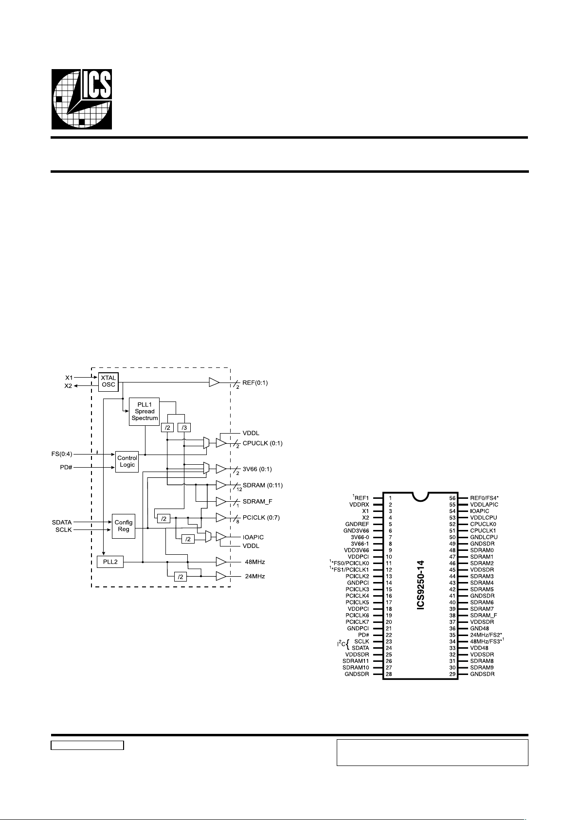
ICS9250-14
Block Diagram
Pentium II is a trademark of Intel Corporation
I2C is a trademark of Philips Corporation
Frequency Timing Generator for Pentium II Systems
9250-14 Rev A 2/5/00
Pin Configuration
Generates the following system clocks:
- 2 - CPUs @ 2.5V, up to 150MHz.
- 1 - IOAPIC @ 2.5V, PCI or PCI/2MHz.
- 13 SDRAMs (3.3V) @ 150MHz.
- 2 - 3V66 @ 3.3V, 2x PCIMHz.
- 8 - PCIs @ 3.3V.
- 1 - 48MHz, @ 3.3V fixed.
- 2 - REF @ 3.3V, 14.318Hz.
- 1 - 24MHz, @ 3.3V fixed.
Supports spread spectrum modulation ,
± .25% center spread.
I
2
C support for power management
Efficient power management scheme through PD#
Uses external 14.138 MHz crystal
56-Pin 300 mil SSOP
The ICS9250-14 is a single chip clock for Intel Pentium II.
It provides all necessary clock signals for such a system.
Spread spectrum may be enabled through I2C programming.
Spread spectrum typically reduces EMI by 8dB to 10 dB.
This simplifies EMI qualification without resorting to board
design iterations or costly shielding. The ICS9250-14
employs a proprietary closed loop design, which tightly
controls the percentage of spreading over process and
temperature variations.
Power Groups
GNDREF, VDDREF = REF, Crystal
GND3V66, VDD3V66 = 3V66
GNDPCI, VDDPCI = PCICLKs
GNDCOR, VDDCOR = PLLCORE
GND48, VDD48 = 48
GNDSDR, VDDSDR = SDRAM
GNDLCPU, VDDLCPU = CPUCLK
GNDLPCI, VDDLAPIC = IOAPIC
1. These pins will have 2X drive strength.
* 120K ohm pull-up to VDD on indicated inputs.
Skew Specifications
CPU CPU: <175ps
SDRAM - SDRAM: < 250ps
3V66 3V66: <250ps
PCI PCI: <500ps
CPU-SDRAM<500ps
CPU(early)-PCI: MIN=1.0ns,TYP=2.0,MAX=4.0
CPU-3V66<500ps
3V66(early)-PCI: MIN=1.5ns,TYP=2.0,MAX=4.0
IOAPIC-PCI<500ps
PRODUCT PREVIEW documents contain information on new
products in the sampling or preproduction phase of development.
Characteristic data and other specifications are subject to change
without notice.
Preliminary Product Preview
2
ICS9250-14
Preliminary Product Preview
Pin Descriptions
NIP
REBMUN
EMANNIPEPYTNOITPIRCSED
11FERTUO.tuptuokcolcecnereferzHM813.41,V3.3
,52,81,01,9,2
54,73,23
DDVRWPylppusrewopV3.3
31XNI
kcabdeefdna)Fp33(pacdaollanretnisah,tupnilatsyrC
2Xmorfrotsiser
42XTUO
daollanretnisaH.zHM813.41yllanimon,tuptuolatsyrC
)Fp33(pac
,12,41,6,5
,63,92,82
94,14
DNGRWPylppusV3.3rofsnipdnuorG
8,7)1;0(66V3TUOBUHrofstuptuokcolczHM66dexiFV3.3
11
0KLCICP
1
TUOSKLCUPCsuonorhcnyShtiw,stuptuokcolcICPV3.3
0SFNI.norewoptadehctaltupnI.tibtcelesycneuqerftupnicigoL
21
1KLCICP
1
NISKLCUPCsuonorhcnyShtiw,stuptuokcolcICPV3.3
1SFNI.norewoptadehctaltupnI.tibtcelesycneuqerftupnicigoL
,61,51,31
02,91,71
)7:2(KLCICPTUOSKLCUPCsuonorhcnyShtiw,stuptuokcolcICPV3.3
22#DPNI
otniecivedehtnwodrewopotdesuniptupniwolevitcasuonorhcnysA
dnaOCVehtdnadelbasideraskcolclanretniehT.etatsrewopwola
ebtonlliwnwodrewopehtfoycnetalehT.deppotseralatsyrceht
.sm3nahtretaerg
32KLCSNIIfotupnikcolC
2
tupniC
42ATADSNIIroftupniataD
2
.tupnilairesC
43
zHM84TUOBSUroftuptuokcolczHM84dexiFV3.3
3SFNI.norewoptadehctaltupnI.tibtcelesycneuqerftupnicigoL
53
2SFNI.norewoptadehctaltupnI.tibtcelesycneuqerftupnicigoL
zHM42TUOtuptuozHM42dexifV3.3
83F_MARDSTUOIybdetceffatonMARDSzHM001gninnureerfV3.3
2
C
,13,03,72,62
,34,24,04,93
84,74,44
)0:11(MARDSTUO
ffodenrutebnacstuptuoMARDSllA.zHM001gninnurtuptuoV3.3
Ihguorht
2
C
05LDNGRWPCIPA&UPCrofylppusrewopV5.2rofdnuorG
25,15)1:0(KLCUPCTUO
SFnognidnepedzHM001rozHM66.tuptuokcolcsubtsoHV5.2
.3egaprefeRsnip)1:0(
55,35LDDVRWPCIPAOI,UPCrofylppyusrewopV5.2
45CIPAOITUO.zHM76.61tagninnurstuptuokcolcV5.2
65
4SFNI.norewoptadehctaltupnI.tibtcelesycneuqerftupnicigoL
0FER
1
TUO.tuptuokcolcecnereferzHM813.41,V3.3
Note:
1. These pins will have 2X drive strength.
3
ICS9250-14
Preliminary Product Preview
Frequency Selection
Clock Enable Configuration
Note:
* These output frequencies are not synchronous to CPUCLK and do not have spread spectrum modulation.
4SF3SF2SF1SF0SF
UPC
zHM
MARDS
zHM
zHM66V3
ICP
zHM
zHMCIPAOI
00000 18.7617.10118.7609.3359.61
00001 00.0700.50100.0700.5305.71
00010 10.2710.80110.2700.6300.81
00011 76.6600.00176.6633.3376.61
00100 10.3715.90110.3705.6352.81
00101 00.5705.21100.5705.7357.81
00110 00.7705.51100.7705.8352.91
00111 10.8710.71110.8700.9305.91
01000 00.0800.02100.0800.0400.02
01001 00.3815.42100.3805.1457.02
01010 94.4847.62194.4852.2421.12
01011 00.00100.05100.00100.0500.52
01100 80.6821.92180.6840.3425.12
01101 00.8800.23100.8800.4400.22
01110 00.0900.53100.0900.5405.22
01111 00.5905.24100.5905.7457.32
10000 09.9409.9462.3336.6123.8
1000 1 00.00100.00166.6633.3376.61
100 10 58.4758.4709.9459.4274.21
100 11 85.6685.6693.4491.2201.11
10 100 48.2848.2832.5516.7218.31
10 10 1 18.9818.9888.9549.9279.41
10 110 08.4908.4902.3606.1308.51
10111 05.00105.00100.7605.3357.61
11000 87.40187.40168.9639.4364.71
11001 77.11177.11125.4762.7336.81
11010 77.41177.41115.6762.8331.91
11011 00.00100.00166.6633.3376.61
11100 57.32157.32105.2852.1426.02
11101 47.23147.23194.8852.4421.22
11110 57.93157.93161.3985.6492.32
11111 96.94196.94197.9909.9459.42
#DPKLCUPCMARDSCIPAOIzHM66KLCICP
,FER
zHM84
csOsOCV
0WOLWOLWOLWOLWOLWOLFFOFFO
1NONONONONONONONO
4
ICS9250-14
Preliminary Product Preview
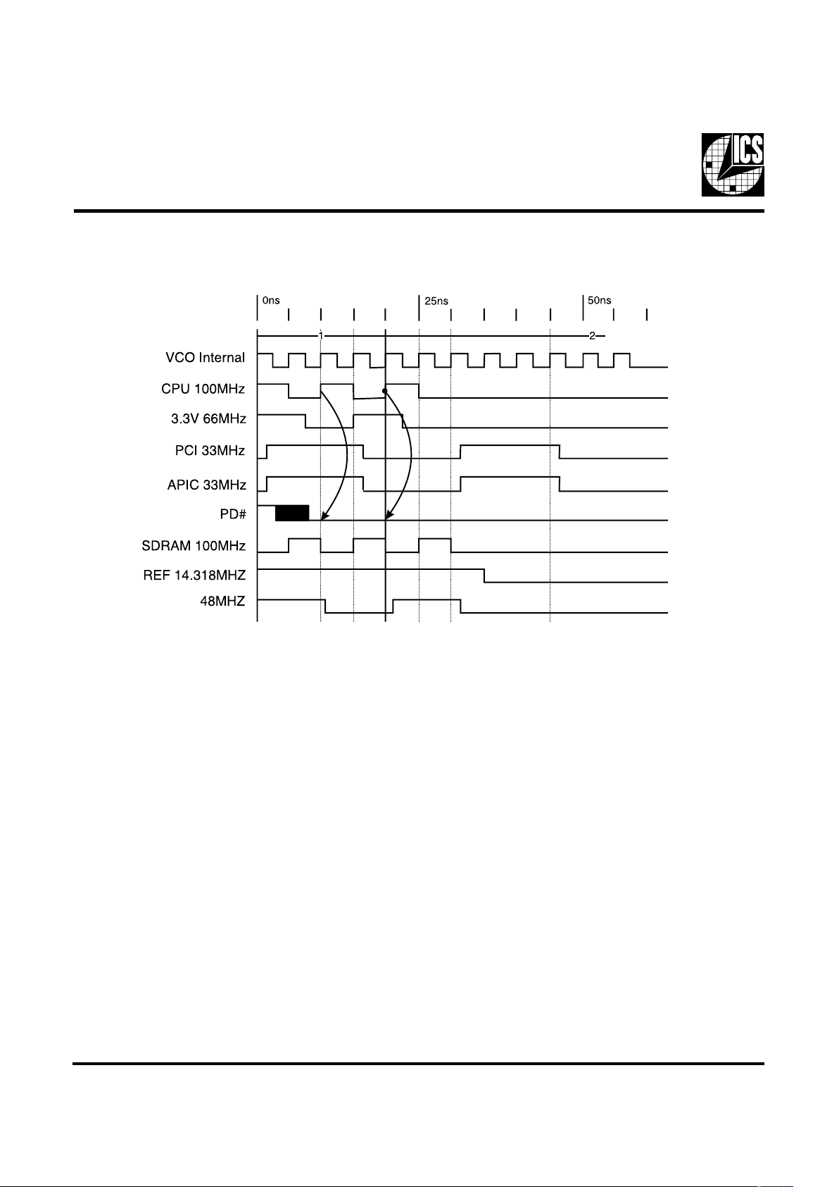
Power Down Waveform
Note
1. After PD# is sampled active (Low) for 2 consective rising edges of CPUCLKs, all
the output clocks are driven Low on their next High to Low tranistiion.
2. Power-up latency <3ms.
3. Waveform shown for 100MHz

5
ICS9250-14
Preliminary Product Preview
1. The ICS clock generator is a slave/receiver, I2C component. It can read back the data stored in the latches for verification.
Read-Back will support Intel PIIX4 "Block-Read" protocol.
2. The data transfer rate supported by this clock generator is 100K bits/sec or less (standard mode)
3. The input is operating at 3.3V logic levels.
4. The data byte format is 8 bit bytes.
5. To simplify the clock generator I2C interface, the protocol is set to use only "Block-Writes" from the controller. The
bytes must be accessed in sequential order from lowest to highest byte with the ability to stop after any complete byte
has been transferred. The Command code and Byte count shown above must be sent, but the data is ignored for those
two bytes. The data is loaded until a Stop sequence is issued.
6. At power-on, all registers are set to a default condition, as shown.
General I2C serial interface information
The information in this section assumes familiarity with I2C programming.
For more information, contact ICS for an I2C programming application note.
How to Write:
Controller (host) sends a start bit.
Controller (host) sends the write address D2
(H)
ICS clock will acknowledge
Controller (host) sends a dummy command code
ICS clock will acknowledge
Controller (host) sends a dummy byte count
ICS clock will acknowledge
Controller (host) starts sending first byte (Byte 0)
through byte 5
ICS clock will acknowledge each byte one at a time.
Controller (host) sends a Stop bit
How to Read:
Controller (host) will send start bit.
Controller (host) sends the read address D3
(H)
ICS clock will acknowledge
ICS clock will send the byte count
Controller (host) acknowledges
ICS clock sends first byte (Byte 0) through byte 5
Controller (host) will need to acknowledge each byte
Controller (host) will send a stop bit
Notes:
Controller (Host) ICS (Slave/Receiver)
Start Bit
Address
D3
(H)
ACK
Byte Count
ACK
Byte 0
ACK
Byte 1
ACK
Byte 2
ACK
Byte 3
ACK
Byte 4
ACK
Byte 5
ACK
Stop Bit
H
ow to Read:
Controller (Host) ICS (Slave/Receiver)
Start Bit
Address
D2
(H)
ACK
Dummy Command Code
ACK
Dummy Byte Count
ACK
Byte 0
ACK
Byte 1
ACK
Byte 2
ACK
Byte 3
ACK
Byte 4
ACK
Byte 5
ACK
Stop Bit
H
ow to Write:

6
ICS9250-14
Preliminary Product Preview
Byte 0: Functionality and frequency select register (Default=0)
(1 = enable, 0 = disable)
Notes:
1. Default at power-up will be for latched logic inputs to define frequency, as diplayed by Bit 3.
tiB
noitpircseD
DWP
tiB
)4:7,2(
)4:7,2(tiB
KLCUPC
zHM
MARDS
zHM
66V3
zHM
KLCICP
CIPAOI
zHM
XXXX
1etoN
00000 18.7617.10118.7609.3359.61
00001 00.0700.50100.0700.5305.71
00010 10.2710.80110.2700.6300.81
00011 76.6600.00176.6633.3376.61
00100 10.3715.90110.3705.6352.81
00101 00.5705.21100.5705.7357.81
00110 00.7705.51100.7705.8352.91
00111 10.8710.71110.8700.9305.91
01000 00.0800.02100.0800.0400.02
01001 00.3815.42100.3805.1457.02
01010 94.4847.62194.4852.2421.12
01011 00.00100.05100.00100.0500.52
01100 80.6821.92180.6840.3425.12
01101 00.8800.23100.8800.4400.22
01110 00.0900.53100.0900.5405.22
01111 00.5905.24100.5905.7457.32
10000 09.9409.9462.3336.6123.8
1000 1 00.00100.00166.6633.3376.61
10010 58.4758.4709.9459.4274.21
10011 85.6685.6693.4491.2201.11
10100 48.2848.2832.5516.7218.31
10101 18.9818.9888.9549.9279.41
10110 08.4908.4902.3606.1308.51
10111 05.00105.00100.7605.3357.61
11000 87.40187.40168.9639.4364.71
11001 77.11177.11125.4762.7336.81
11010 77.41177.41115.6762.8331.91
11011 00.00100.00166.6633.3376.61
11100 57.32157.32105.2852.1426.02
11101 47.23147.23194.8852.4421.22
11110 57.93157.93161.3985.6492.32
11111 96.94196.94197.9909.9459.42
3tiB
stupnidehctal,tceleserawdrahybdetcelessiycneuqerF-0
4:6,2tiBybdetcelessiycneuqerF-1
0
1tiB
lamroN-0
daerpSretneC%52.0±elbanemurtcepsdaerpS-1
1
0tiB
gninnuR-0
stuptuollaetatsirT-1
0

7
ICS9250-14
Preliminary Product Preview
Byte 1: Control Register
(1 = enable, 0 = disable)
Notes:
1. Inactive means outputs are held LOW and are disabled from switching. These outputs are designed to be configured
at power-on and are not expected to be configured during the normal modes of operation.
2. PWD = Power on Default
tiB#niPDWPnoitpircseD
7tiB-X #3SF
6tiB-X #0SF
5tiB-X #2SF
4tiB531 zHM84_42
3tiB-1 )devreseR(
2tiB431 zHM84
1tiB-1 )devreseR(
0tiB831 F_MARDS
tiB#niPDWPnoitpircseD
7tiB021 7KLCICP
6tiB911 6KLCICP
5tiB711 5KLCICP
4tiB611 4KLCICP
3tiB511 3KLCICP
2tiB31
1
2KLCICP
1tiB211 1KLCICP
0tiB111 0KLCICP
Byte 3: Control Register
(1 = enable, 0 = disable)
Byte 2: Control Register
(1 = enable, 0 = disable)
tiB#niPDWPnoitpircseD
7tiB931 7MARDS
6tiB041 6MARDS
5tiB241 5MARDS
4tiB341 4MARDS
3tiB441 3MARDS
2tiB64
1
2MARDS
1tiB741 1MARDS
0tiB841 0MARDS
tiB#niPDWPnoitpircseD
7tiB-1 )devreseR(
6tiB71 0_66V3
5tiB81 0_66V3
4tiB-X #4SF
3tiB451 CIPAOI
2tiB-X #1SF
1tiB151 1KLCUPC
0tiB251 0KLCUPC
Byte 4: Control Register
(1 = enable, 0 = disable)
tiB#niPDWPnoitpircseD
7tiB-1 )devreseR(
6tiB-1 )devreseR(
5tiB-1 )devreseR(
4tiB-1 )devreseR(
3tiB621 11MARDS
2tiB721 01MARDS
1tiB031 9MARDS
0tiB131 8MARDS
Byte 5: Control Register
(1 = enable, 0 = disable)

8
ICS9250-14
Preliminary Product Preview
Absolute Maximum Ratings
Core Supply Voltage . . . . . . . . . . . . . . . . . . . . . . 4.6 V
I/O Supply Voltage . . . . . . . . . . . . . . . . . . . . . . . 3.6V
Logic Inputs . . . . . . . . . . . . . . . . . . . . . . . . . . . . GND 0.5 V to VDD +0.5 V
Ambient Operating Temperature . . . . . . . . . . . . 0°C to +70°C
Storage Temperature . . . . . . . . . . . . . . . . . . . . . . 65°C to +150°C
Case Temperature . . . . . . . . . . . . . . . . . . . . . . . . 115°C
Stresses above those listed under Absolute Maximum Ratings may cause permanent damage to the device. These ratings are
stress specifications only and functional operation of the device at these or any other conditions above those listed in the
operational sections of the specifications is not implied. Exposure to absolute maximum rating conditions for extended
periods may affect product reliability.
Electrical Characteristics - Input/Supply/Common Output Parameters
TA = 0 - 70C; Supply Vol ta ge VDD = 3.3 V +5%, V DDL=2.5 V + 5%(un less otherwise state d )
PARAMETER SY MBOL CONDITIONS MIN TYP MAX UNITS
Input High Voltage V
IH
2V
DD
+0.3 V
In put Low Voltage V
IL
VSS-0.3 0.8 V
Input High Current I
IH
VIN = V
DD
-5 5
µ
A
Input Low Current I
IL1
VIN = 0 V; Inputs with no pull -up resistor s -5 2.0
µ
A
Input Low Current I
IL2
VIN = 0 V; Inputs with pull -up resistor s -200 -100
µ
A
Operating I
DD3.3OPCL
= 0 pF; Select @ 66M 60 100 mA
Supply Current
Power Down I
DD3.3PDCL
= 0 pF; With inp ut address to Vdd or GND 400 600
µ
A
Supply Current
Input frequenc y F
i
VDD = 3.3 V; 14.318 MHz
Pin Inductance L
pin
7nH
Input Capacitance
1
C
IN
Logic Inputs 5 pF
C
out
O ut put pin capac itance 6 pF
C
INX
X1 & X2 pins 13.5 22.5 pF
Transition Time
1
T
trans
To 1st crossing of target Fr eq. 3 mS
Settling Time
1
T
s
From 1st crossing to 1 % ta rget Fre q. mS
Clk Stabilization
1
T
STAB
From VDD = 3.3 V to 1% target Freq. 3 mS
Delay t
PZH,tPZH
output ena ble delay (all outputs) 1 1 0 nS
t
PLZ,tPZH
output disable del ay (al l outputs) 1 10 nS
1
Guar e nt eed by de sign, not 100% tested in produc t ion.

9
ICS9250-14
Preliminary Product Preview
Elect r i cal C har act er i st ics - 3V 66
TA = 0 - 70C; VDD = 3.3 V +/-5%; CL = 1 0-30 pF ( unle s s otherwise sta ted)
PARA METER SYMBOL CONDITIONS MIN TYP MAX UNITS
O utput Freque ncy F
O
1
66 MHz
O utput Impedanc e R
DSP1
1
VO = VDD*(0.5) 12 55
Ω
O utput Impedanc e R
D
SN1
1
VO = V
D
D
*(0.5) 12 55
Ω
Output High Voltage V
O
H1
I
O
H
= -1 mA 2.4 V
Output Low Voltage V
O
L1
I
O
L
= 1 mA 0.5 5 V
O utput High Curr e nt I
O
H1
V
OH@ MIN = 1.0 V, VOH@ MAX = 3.135 V -33 -33 mA
O utput L o w Current I
O
L1
VOL@ MIN = 1.95 V, VOL@ MAX= 0.4 30 38 mA
Rise Time t
r
1
1
V
O
L
= 0. 4 V, V
O
H
= 2 .4 V 0.4 1.6 ns
Fa ll T ime t
f1
1
VOH = 2.4 V, VOL = 0 .4 V 0.4 1.6 ns
Duty Cycle d
t
1
1
VT = 1.5 V 45 55 %
Skew t
s
k1
1
VT = 1.5 V 175 ps
Jitter t
j
cyc-cyc
VT = 1.5 V 500 ps
1
G ua renteed by des ign, not 100% tes te d in production.
Electrical Characteristics - CPU
TA = 0 - 70C, V
DDL
= 2.5 V + / -5%; CL = 1 0 - 20 pF ( unle ss otherwise s ta te d)
PARA METER SYMBOL CONDITIONS MIN TYP MAX UNITS
O utput Freque ncy F
O
2
66 100 MHz
O utput Impeda nc e R
D
SP2B
1
VO = V
D
D
*(0.5) 13.5 45
Ω
O utput Impeda nc e R
DSN2B
1
VO = VDD*(0.5) 13.5 45
Ω
Output High Voltage V
OH2B
IOH = -1 mA 2 V
Output Low Voltage V
O
L2B
I
O
L
= 1 mA 0.4 V
O utput High Curr e nt I
O
H2B
V
O
H @MIN
= 1.0V , V
O
H@ MAX
= 2 .375V -27 -27 mA
O utput L o w Current I
O
L2B
V
O
L @MIN
= 1.2V , V
O
L@ MAX
= 0.3V 27 30 mA
Rise Time t
r
2B
1
V
O
L
= 0. 4 V, V
O
H
= 2 .0 V 0.4 1.6 ns
Fa ll T ime t
f2B
1
VOH = 0.4 V, VOL = 2 .0 V 0.4 1.6 ns
Duty Cycle d
t
2B
1
VT = 1.25 V 455055ns
Skew t
s
k2B
1
VT = 1.25 V 175 ps
t
jcyc-cyc
1
VT = 1.25 V 250 ps
Jitter
1
G ua renteed by des ign, not 100% tes te d in production.

10
ICS9250-14
Preliminary Product Preview
Electrical Characteristics - IOAPIC
TA = 0 - 70C;V
DDL
= 2. 5 V +/- 5% ; CL = 10 - 20 pF ( u nless otherwise s ta te d)
PARA METER SYMBOL CONDITIONS MIN TYP MAX UNITS
O utput Frequency F
O
4
16.67 MHz
O utput Frequency F
O
5
33 MHz
O utput Impedanc e R
D
SP4B
1
VO = V
D
D
*(0.5) 9 30
Ω
O utput Impedanc e R
D
SN4B
1
VO = V
D
D
*(0.5) 9 30
Ω
Output High Voltage V
O
H4\B
I
O
H
= -5.5 mA 2 V
Output Low Voltage V
O
L4B
I
O
L
= 9.0 mA 0.4 V
O utput High Curr e nt I
O
H4B
V
O
H@ mi n
= 1.4 V, V
O
H@ MAX
= 2 .5 V -36 -21 m A
O utput L o w Current I
O
L4B
V
O
L@ MIN
= 1.0 V, V
O
L@ MAX=
0.2 36 31 mA
Rise Time t
r
4B
1
V
O
L
= 0. 4 V, V
O
H
= 2 .0 V 0.4 1.6 nS
Fa ll T ime t
f
4B
1
V
O
H
= 2.0 V, V
O
L
= 0 .4 V 0.4 1.6 nS
Duty Cycle d
t
4B
1
VT = 1.25 V 45 55 %
Jitter t
jcyc-cyc
VT = 1.25 V 500 pS
1
G uarenteed by de s ign, not 100% tes te d in production.
Electrical Characteristics - SDRAM
TA = 0 - 70C; VDD = V
DDL
= 3.3 V +/-5%; CL = 20 - 30 pF (unless otherwise stated)
PARAMETER SY MBOL CONDITIONS MIN TYP MAX UNITS
O utpu t Freque nc y F
O3
100 MHz
O utp ut Impedance R
DSP3
1
VO = VDD*(0.5) 10 24
Ω
O utp ut Impedance R
DSN3
1
VO = VDD*(0.5) 10 24
Ω
O utput High Voltage V
OH3
IOH = -1 mA 2.4 V
Output Low V oltage V
OL3
IOL = 1 mA 0.4 V
Ou tput Hig h Current I
OH3
V
OH @MI N
= 2.0 V , V
OH@ MAX
=3.13 5 V -54 - 4 6 m A
Output Low Current I
OL3
V
OL@ MIN
= 1.0 V , V
OL@ MAX
=0.4 V 54 53 mA
Rise Time T
r3
1
VOL = 0.4 V, VOH = 2.4 V 0.4 1.6 ns
Fall Time T
f3
1
VOH = 2.4 V , VOL = 0.4 V 0.4 1.6 ns
Duty Cycle D
t3
1
VT = 1.5 V 45 55 %
Skew T
sk3
1
VT = 1.5 V 250 ps
Jitter t
j
cyc-cyc VT = 1.5 V 250 ps
1
Guar e nt eed by de sign, not 100% tested in produc t ion.

11
ICS9250-14
Preliminary Product Preview
Elect r i cal C har act er i st ics - P CI
TA = 0 - 70C; VDD = 3.3 V +/-5%; CL = 1 0-30 pF ( unle s s otherwise sta ted)
PARA METER SYMBOL CONDITIONS MIN TYP MAX UNITS
O utput Freque ncy F
O
1
33 MHz
O utput Impedanc e R
DSP1
1
VO = VDD*(0.5) 12 55
Ω
O utput Impedanc e R
D
SN1
1
VO = V
D
D
*(0.5) 12 55
Ω
Output High Voltage V
O
H1
I
O
H
= -1 mA 2.4 V
Output Low Voltage V
O
L1
I
O
L
= 1 mA 0.5 5 V
O utput High Curr e nt I
O
H1
V
OH@ MIN = 1.0 V, VOH@ MAX = 3.135 V -33 -33 mA
O utput L o w Current I
O
L1
VOL@ MIN = 1.95 V, VOL@ MAX= 0.4 30 38 mA
Rise Time t
r
1
1
V
O
L
= 0. 4 V, V
O
H
= 2.4 V 0.5 2 ns
Fa ll T ime t
f1
1
VOH = 2.4 V, VOL = 0.4 V 0.5 2 ns
Duty Cycle d
t
1
1
VT = 1.5 V 45 55 %
Skew t
s
k1
1
VT = 1.5 V 500 ps
Jitter t
j
cyc-cyc
VT = 1.5 V 500 ps
1
G ua renteed by des ign, not 100% tes te d in production.
Electrical Characteristics - 48M, REF
TA = 0 - 70C; VDD = V
DDL
= 3.3 V +/-5%; CL = 10 -20 pF ( unless otherwise stat e d)
PARAMETER SY MBOL CONDITIONS MIN TYP MAX UNITS
O utpu t Freque nc y F
O48M
48 MHz
O utpu t Freque nc y F
OREF
14.318 MHz
O utp ut Impedan c e R
DSP5
1
VO = VDD*(0.5) 20 60
Ω
O utp ut Impedan c e R
DSN5
1
VO = VDD*(0.5) 20 60
Ω
O utput High Voltage V
OH5
IOH = 1 mA 2.4 V
Output Low Voltage V
OL5
IOL = -1 m A 0.4 V
Ou tput High Current I
OH5
V
OH @MIN
=1 V, V
OH@MAX
= 3.135 V -29 -23 mA
Output Low Current I
OL5
V
OL@MIN
=1.95 V, V
OL@MIN
=0.4 V 29 27 mA
Rise Time t
r5
1
VOL = 0.4 V, VOH = 2.4 V 1.8 4 nS
Fall Time t
f5
1
VOH = 2.4 V , VOL = 0.4 V 1.7 4 nS
Duty Cycle d
t5
1
VT = 1.5 V 45 55 %
Jitter t
jcyc-cyc
1
VT = 1.5 V; Fixed Clocks 500 pS
t
jcyc-cyc
1
VT = 1.5 V ; Ref Clocks 1000 pS
Skew T
sk
VT = 1.5 V 250 pS
1
Guar e nt e e d by de sign, not 100% tested in product ion.

12
ICS9250-14
Preliminary Product Preview
Group Offset Waveforms
Gr oup Skew s at C om m on Transiti on Edges:
CP U & IOA PIC loa d (lumped) = 20pf; PCI, SDRAM, 3V66 LOA D (L UMPE D) = 30pf.
GROUP SYMBOL CONDITIONS MIN TYP MAX UNITS
CPU (at 66MHz) to
3V66
S
CPU1-3V66
CP U @ 1. 25V, 3V66 @ 1. 5V (Note: 180°
offset between CP U & 3V 66
0500ps
CPU (at 100MHz) to
SDRAM
S
CPU2-SDRAM
C
PU @ 1. 2 5V, S DRA M @ 1.5V (N ote : 180°
offset between CP U & S DRAM
0500ps
3V 66 t o PCI S
3V66-PCI
3V 66 @ 1.5V , PCI @ 1.5V 1.5 2.1 4 ns
IOAPIC to PCI S
IOAPIC-PCI
IOAPIC @ 1.25V, PCI @1.5V 0 500 ps

13
ICS9250-14
Preliminary Product Preview
PRODUCT PREVIEW documents contain information on new
products in the sampling or preproduction phase of development.
Characteristic data and other specifications are subject to change
without notice.
LOBMYSSNOISNEMIDNOMMOCSNOITAIRAVDN
.NIM.MON.XAM.NIM.MON.XAM
A590.201.011.DA027.527.037.65
1A800.210.610.
2A780.090.490.
B800.- 5310.
c500.-010.
DsnoitairaVeeS
E192.592.992.
eCSB520.0
H593.-024.
h010.310.610.
L020.-040.
NsnoitairaVeeS
µ
°0- °8
56 Pin 300 mil SSOP Package
“For current dimensional specifications, see JEDEC 95.”
.093
DIA. PIN (Optional)
D/2
E/2
BOTTOM VIEW
A
2
SEE
DETAIL “A”
-E-
c
END VIEW
H
Pin 1
TOP VIEW
Index
Area
PARTING LINE
L
DETAIL “A”
A
1
-e-
B
A
SIDE VIEW
-C-
-D-
SEATING
PLANE
.004
C
Ordering Information
ICS9250yF-14-T
Designation for tape and reel packaging
Pattern Number (2 or 3 digit number for parts with ROM code patterns)
Package Type
F=SSOP
Revision Designator (will not correlate with datasheet revision)
Device Type (consists of 3 or 4 digit numbers)
Prefix
ICS, AV = Standard Device
Example:
ICS XXXX y F - PPP - T
Dimensions in inches
 Loading...