

General Description Features
ICS9250-12
Integrated
Circuit
Systems, Inc.
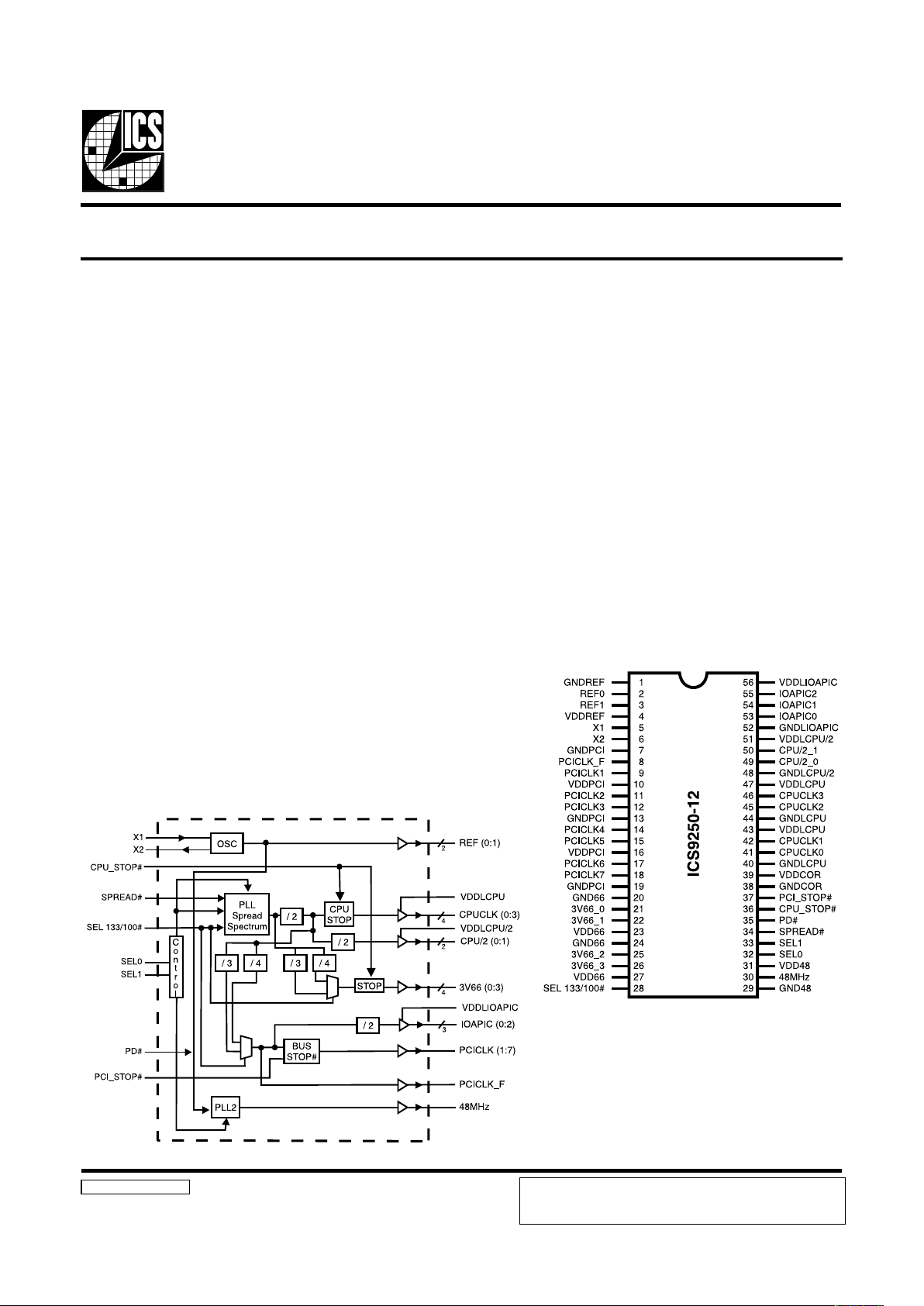
Block Diagram
Frequency Timing Generator for PENTIUM II/III Systems
9250-12 Rev B 2/23/00
Pin Configuration
56-pin SSOP
Generates the following system clocks:
- 4 CPU clocks ( 2.5V, 100/133MHz)
- 8 PCI clocks, including 1 free-running (3.3V, 33MHz)
- 2 CPU/2 clocks (2.5V, 50/66MHz)
- 3 IOAPIC clocks (2.5V, 16.67MHz)
- 4 Fixed frequency 66MHz clocks(3.3V, 66MHz)
- 2 REF clocks(3.3V, 14.318MHz)
- 1 USB clock (3.3V, 48MHz)
Efficient power management through PD#, CPU_STOP#
and PCI_STOP#.
0.5% typical down spread modulation on CPU, PCI,
IOAPIC, 3V66 and CPU/2 output clocks.
Uses external 14.318MHz crystal.
The ICS9250-12 is a main clock synthesizer chip for
Pentium II based systems using Rambus Interface DRAMs.
This chip provides all the clocks required for such a system
when used with a Direct Rambus Clock Generator (DRCG)
chip such as the ICS9212-01, 02, 03 and a PCI buffer 9112-17.
Spread Spectrum may be enabled by driving the SPREAD#
pin active. Spread spectrum typically reduces system EMI
by 8dB to 10dB. This simplifies EMI qualification without
resorting to board design iterations or costly shielding. The
ICS9250-12 employs a proprietary closed loop design,
which tightly controls the percentage of spreading over
process and temperature variations.
The CPU/2 clocks are inputs to the DRCG.
Key Specification:
CPU Output Jitter: 150ps
IOAPIC Output Jitter: 250ps
CPU/2, 3V66, PCI Output Jitter: 250ps
CPU (0:3) CPU/2 Output Skew: <175ps
PCI_F, PCI 1:7 Output Skew: <500ps
3V66 (0:3) Output Skew <250ps
IOAPIC (0:2) Output Skew <250ps
CPU to 3V66 (0:3) Output Offset: 0.0 - 1.5ns (CPU leads)
CPU to PCI Output Offset: 1.5 - 4.0ns (CPU leads)
CPU to APIC Output Offset 1.5 - 4.0ns (CPU leads)
ICS reserves the right to make changes in the device data identified in
this publication without further notice. ICS advises its customers to
obtain the latest version of all device data to verify that any
information being relied upon by the customer is current and accurate.
2
ICS9250-12
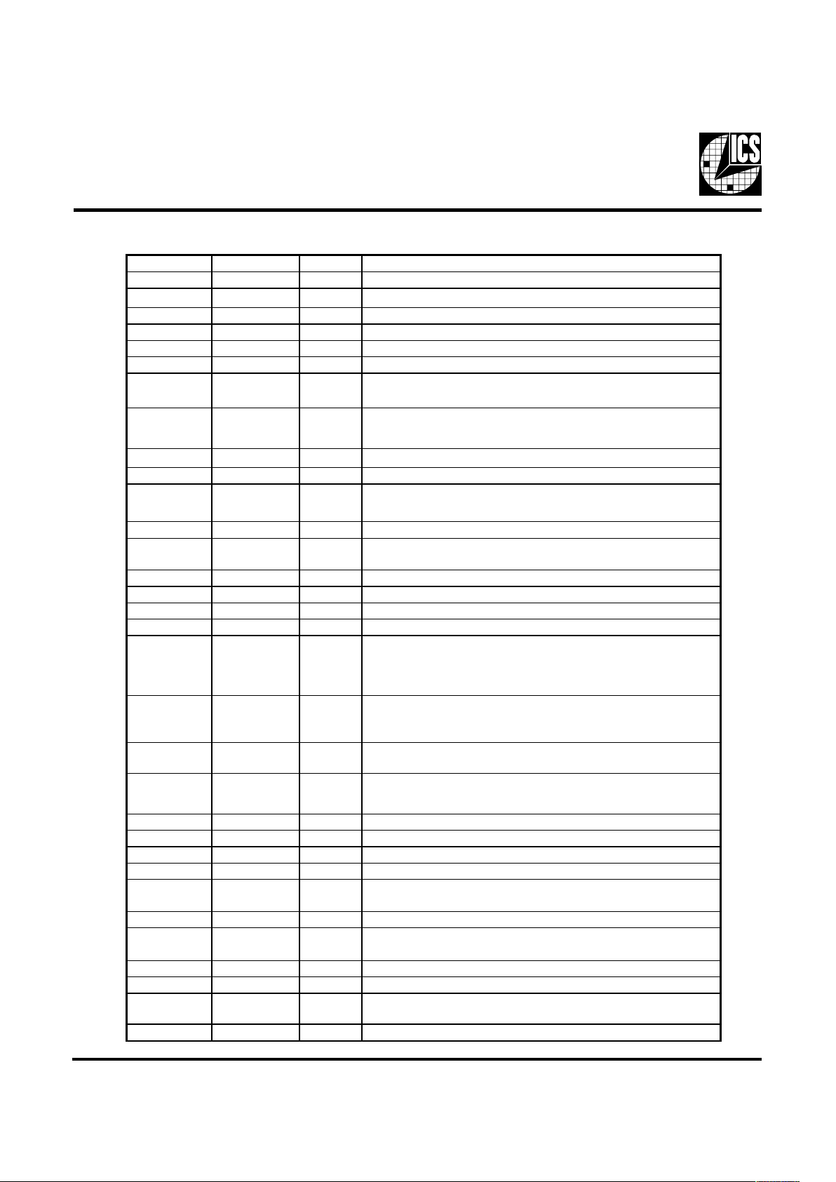
Pin Descriptions
Pin number Pin name Type Description
1 GN DREF PWR Gnd pin for R EF clocks
2, 3 REF(0:1) OUT 14.318MH z reference clock outputs at 3.3V
4 VDDREF PWR Power pin for REF clocks
5 X1 IN XTAL_IN 14.318MHz crystal input
6 X2 OUT XTAL _OUT Cr ystal output
7, 13, 19 GNDPCI PWR Gnd pin for PCICLKs
8 PCICLK_F OUT
Free running PCI clock at 3.3V. Synchronous to CPU clocks. Not affected
by the PCI_STOP# input.
9, 11, 12, 14, 15,
17, 18
PCICLK[1:7] OUT PC I clock outputs at 3.3V. Synchronous to CPU clocks.
10, 16 VDDPCI PWR 3.3Volts power pin for PCICLKs
20, 24 GND66 P WR Gnd pin for 3V66 outputs
21, 22, 25, 26 3V66[0:3] OUT
66MHz outputs at 3.3V. These outputs are stopped when CPU_S TOP# is
driven active..
23, 27 VDD66 PWR power pin for the 3V66 clocks.
28 SEL 133/100# IN
This selects the frequency fo r the CPU and CPU/2 outputs. High =
133MHz, Low=100MHz
29 G ND48 PWR G round pin for the 48M Hz output
30 48M Hz OUT Fixed 48MHz clock output. 3.3V
31 V DD48 PWR P o wer pin for the 48MHz output.
32, 33 SEL[0:1] IN F unction select pins. See truth table for details.
34 S P READ # IN
Enables spread spectrum when active(Low). modulates all the CP U, PCI,
IOAP IC, 3V66 and CPU/2 clocks. Does not affect the REF and 48MHz
clocks. 0.5% down spread modulation.
35 PD# IN
This asyn chronous input powers down the chip when drive active(Lo w).
The internal PLLs are disabled and all the output clocks are held at a Low
state.
36 CPU_STOP# IN
This asychronous input halts the CPUCLK[0:3] and the 3V66[0:3] clocks at
l
ogic "0" when driven active( Low). Does not affect the CPU/2 clocks.
37 PCI_STOP# IN
This asynchronous input halts the PCICLK[1:7] at logic"0" when driven
active(Low). PCICLK_F is not affected by this input.
38 G NDCOR PWR Ground pin for the PLL core
39 V DDCOR PWR P ower pin for the PLL core. 3.3V
43, 47 VDDLCPU PWR Pow er pin for the CP UCLKs. 2.5V
40, 44 GNDLCPU PWR Ground pin for the CPU C LKs
41, 42, 45, 46 CPUCLK[0:3] OUT
Host bus clock output at 2.5V. 133MHz or 100MHz depending on the state
of the SEL 133/100MHz.
48 GNDLCPU/2 PWR Ground pin for the CPU/2 clocks.
49, 50 CPU/2[0:1] OUT
2.5V clock outputs at 1/2 CPU frequency. 66MHz or50MHz depending on
the state of the SEL 133/100# input pin.
51 V DDLCPU/2 PWR Power pin for the CPU /2 clocks. 2.5V
52 G NDLIOAPIC PWR Ground pin for the IOAPIC outputs.
53, 54, 55 IOAPIC[0:2] OUT
IOAPIC clocks at 2.5V. Synchronous with CPUCLKs but fixed at
16.67MHz.
56 V DDLIOAP IC PWR Pow er pin for the IO APIC outputs. 2.5V.
3
ICS9250-12
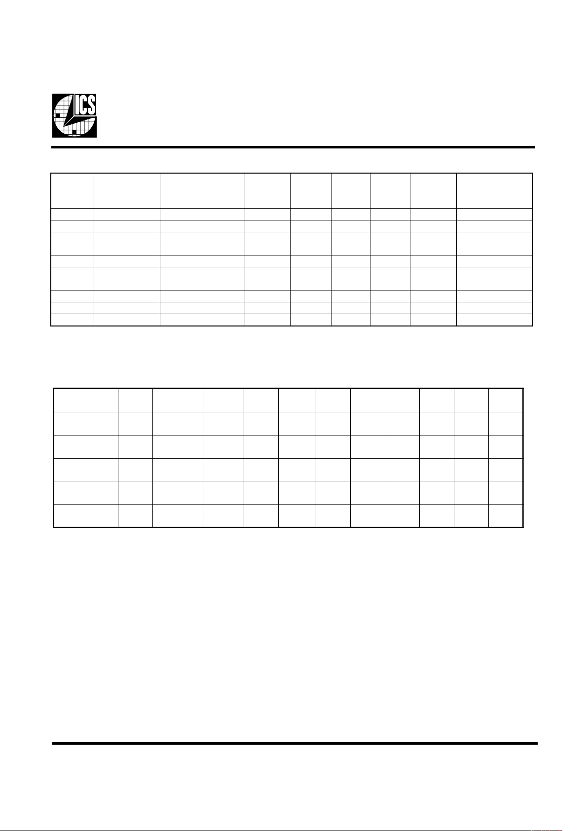
Frequency Select:
Note:
1. TCLK is a test clock driven on the x1 input during test mode.
#POTS_UPC#DP#POTS_ICPKLCUPC2/UPCCIPAOI66V3ICPF_ICP
.FER
zHM84
csOsOCV
X0XWOLWOLWOLWOLWOLWOLWOLFFOFFO
010WOLNONOWOLWOLNONONONO
011WOLNONOWOLNONONONONO
110NONONONOWOLNONONONO
111NONONONONONONONONO
ICS9250-12 Power Management Features:
Note:
1. LOW means outputs held static LOW as per latency requirement next page.
2. On means active.
3. PD# pulled Low, impacts all outputs including REF and 48 MHz outputs.
4. All 3V66 as well as all CPLU clocks should stop cleanly when CPU_STOP# is pulled LOW.
5. CPU/2, IOAPIC, REF, 48 MHz signals are not controlled by the CPU_STOP# functionality and are enabled all in all conditions
except PD# = LOW
Power Groups:
VDDREF, GNDREF = REF, X1, X2
GNDPCI, VDDPCI = PCICLK
VDD66, GND66 = 3V66
VDD48, GND48 = 48MHz
VDDCOR, GNDCOR = PLL Core
VDDLCPU/2 , GNDLCPU/2 = CPU/2
VDDLIOAPIC, GNDIOAPIC = IOAPIC
LES
-001/331
#
1LES0LES
UPC
zHM
2/UPC
zHM
66V3
zHM
ICP
zHM
84
zHM
FER
zHM
CIPAOI
zHM
stnemmoC
000 Z-iHZ-iHZ-iHZ-iHZ-iHZ-iHZ-iHetats-irT
001A/NA/NA/NA/NA/NA/NA/NdevreseR
010 001056633Z-iH813.4176.61
LLPzHM84
delbasid
011 00105663384813.4176.61
100 2/KLCT4/KLCT4/KLCT8/KLCT
-/KLCT
2
KLCT61/KLCT)1(edomtseT
101 A/NA/NA/NA/NA/NA/NA/NdevreseR
110 331666633Z-iH813.4176.61
111 33166663384813.4176.61

4
ICS9250-12
Power Management Requirements:
Note:
1. Clock on/off latency is defined in the number of rising edges of free running PCICLKs between the clock disable goes low/
high to the first valid clock comes out of the device.
2. Power up latency is when PWR_DWN# goes inactive (high to when the first valid clocks are dirven from the device.
lagniSetatSlagniS
ycnetaL
fosegdegnisirfo.oN
KLCICP
POTS_UPC
)delbasid(01
)delbane(11
#POTS_ICP
)delbasid(01
)delbane(11
#DP
)noitarepolamron(1Sm3
)nwodrewop(0.xam2
CPU_STOP# Timing Diagram
CPU_STOP# is an asynchronous input to the clock synthesizer. It is used to turn off the CPU and 3V66 clocks for low power
operation. CPU_STOP# is asserted asynchronously by the external clock control logic with the rising edge of free running PCI
clock (and hence CPU clock) and must be internally synchronized to the external output. All other clocks will continue to run
while the CPU clocks are disabled. The CPU clocks must always be stopped in a low state and started in such a manner as to
guarantee that the high pulse width is a full pulse. ONLY one rising edge of PCICLK_F is allowed after the clock control logic
switched for both the CPU and 3V66 outputs to become enabled/disabled.
Notes:
1. All timing is referenced to the internal CPUCLK.
2. The internal label means inside the chip and is a reference only. This
in fact may not be the way that the control is designed.
3. CPU_STOP# signal is an input singal that must be made synchronous
to free running PCICLK_F
4. 3V66 clocks also stop/start before
5. PD# and PCI_STOP# are shown in a high state.
6. Diagrams shown with respect to 133MHz. Similar operation when CPU
is 100MHz

5
ICS9250-12
PCI_STOP# Timing Diagram
PCI_STOP# is an input to the clock synthesizer and must be made synchronous to the clock driver PCICLK_F output. It is used
to turn off the PCI clocks for low power operation. PCI clocks are required to be stopped in a low state and started such that a
full high pulse width is guaranteed. ONLY one rising edge of PCICLK_F is allowed after the clock control logic switched for the
PCI outputs to become enabled/disabled.
Notes:
1. All timing is referenced to CPUCLK.
2. PCI_STOP# signal is an input signal which must be made synchronous to PCICLK_F output.
3. Internal means inside the chip.
4. All other clocks continue to run undisturbed.
5. PD# and CPU_STOP# are shown in a high state.
6. Diagrams shown with respect to 133MHz. Similar operation when CPU is 100MHz.

6
ICS9250-12
PD# Timing Diagram
The power down selection is used to put the part into a very low power state without turning off the power to the part. PD# is
an asynchronous active low input. This signal needs to be synchronized internal to the device prior to powering down the clock
synthesizer.
Internal clocks are not running after the device is put in power down. When PD# is active low all clocks need to be driven to a
low value and held prior to turning off the VCOs and crystal. The power up latency needs to be less than 3 mS. The power down
latency should be as short as possible but conforming to the sequence requirements shown below. PCI_STOP# and CPU_STOP#
are considered to be don't cares during the power down operations. The REF and 48MHz clocks are expected to be stopped in
the LOW state as soon as possible. Due to the state of the internal logic, stopping and holding the REF clock outputs in the
LOW state may require more than one clock cycle to complete.
Notes:
1. All timing is referenced to the Internal CPUCLK (defined as inside the ICS9250 device).
2. As shown, the outputs Stop Low on the next falling edge after PD# goes low.
3. PD# is an asynchronous input and metastable conditions may exist. This signal is synchronized inside this part.
4. The shaded sections on the VCO and the Crystal signals indicate an active clock.
5. Diagrams shown with respect to 133MHz. Similar operation when CPU is 100MHz.

7
ICS9250-12
Absolute Maximum Ratings
Supply Voltage . . . . . . . . . . . . . . . . . . . . . . . . . . . 7.0 V
Logic Inputs . . . . . . . . . . . . . . . . . . . . . . . . . . . . GND 0.5 V to VDD +0.5 V
Ambient Operating Temperature . . . . . . . . . . . . 0°C to +70°C
Storage Temperature . . . . . . . . . . . . . . . . . . . . . . 65°C to +150°C
Stresses above those listed under Absolute Maximum Ratings may cause permanent damage to the device. These ratings are
stress specifications only and functional operation of the device at these or any other conditions above those listed in the
operational sections of the specifications is not implied. Exposure to absolute maximum rating conditions for extended periods
may affect product reliability.
Electrical Characteristi cs - I nput/Supply/Common Output Parameters
TA = 0 - 70º C; Supply Voltage VDD = 3.3 V +/-5%, V
DDL
= 2.5 V +/-5% (unless otherwise stated)
PARAMETER
S
YMBOL
C
ONDITIONS MIN TYP MAX UNITS
Input High Voltage V
I
H
2V
DD
+0.3 V
Input Low Voltage V
I
L
V
S
S
-0.3 0.8 V
Input High Current I
I
H
V
I
N
= V
DD
0.1 5
µ
A
Input Low Current I
I
L1
V
I
N
= 0 V; Inputs with no pull-up resistors -5 2.0
µ
A
Input Low Current I
I
L2
V
I
N
= 0 V; Inputs with pull-up re si stors -200 -100
µ
A
Operating I
DD3.3OP100
Select @ 100MHz; Max discr ete cap loads 68
180
Supply Current I
DD3.3OP133
Select @ 133MHz; Max discr ete cap loads 80
Power Down I
DD3.3PD
CL = 0 pF; PWRDWN# = 0
Supply Current
Input frequency F
i
VDD = 3.3 V 12 14. 318 16 MHz
Input Capacitance
1
C
I
N
Logic Inputs 5 pF
C
I
NX
X1 & X2 pins 27 36 45 pF
Transition Time
1
T
Trans
To 1st crossing of targe t Fr eq. 3 ms
Settling Time
1
T
S
From 1st crossing to 1% target Fre q. 1 ms
C
lk Stabilization
1
T
Stab
From VDD = 3.3 V to 1% target Freq.
3ms
1
Guaranteed by design, not 100% tested in production.
uA20062
mA
Electrical Characteristics - Input/ Suppl y/Common Output Parameters
TA = 0 - 70º C; Supply Voltage VDD = 3.3 V +/-5%, V
DDL
= 2.5 V +/-5% (unless otherwise stated)
PARAMETER SYMBOL CONDIT IONS MIN TYP MAX UNITS
Operating I
DD2.5OP100
Select @ 100MHz; Max discrete cap loads 19
25
Supply Current
I
DD2.5OP133
Select @ 133MHz; Max discrete cap loads 22
40
1
Guaranteed by design, not 100% tested in production.
mA

8
ICS9250-12
Electrical Characteristics - CPUCLK
TA = 0 - 70º C; VDD = 3.3 V +/-5%, V
DDL
= 2.5 V +/-5%; CL = 20 pF (unless otherwise stated)
PARAMETER SYMBOL CON DITIONS MIN TYP MAX UNITS
Output High Voltage V
OH2B
IOH = -12.0 mA 2 2.2 V
Output Low Voltage V
OL2B
IOL = 12 mA 0.3 0.4 V
Output High Current I
OH2B
VOH = 1.7 V -35 -19 mA
Output Low Current I
OL2B
VOL = 0.7 V 19 27 mA
Rise Time t
r2B
1
VOL = 0.4 V, VOH = 2.0 V 0.4 1.2 1.6 ns
Fall Time t
f2B
1
VOH = 2.0 V, VOL = 0.4 V 0.4 1.25 1.6 ns
Duty Cycle d
t2B
1
VT = 1.25 V 45 48 55 %
Skew t
sk2B
1
VT = 1.25 V 80 175 ps
Jitter, Absolute t
jabs2B
1
VT = 1.25 V -150 61 +150 ps
Jitter, Cycle-to-cycle
t
jcyc-cyc2B
1
VT = 1.25 V
100 150 ps
1
Guaranteed by design, not 100% tested in production.
Electrical Characteristics - CPU/2
TA = 0 - 70º C; VDD = 3.3 V +/-5%, V
DDL
= 2.5 V +/-5%; CL = 20 pF (unless otherwise stated)
PARAMETER SYMBOL CON DITIONS MIN TYP MAX UNITS
Output High Voltage V
OH2B
IOH = -12.0 mA 2 2.3 V
Output Low Voltage V
OL2B
IOL = 12 mA 0.3 0.4 V
Output High Current I
OH2B
VOH = 1.7 V -35 -19 mA
Output Low Current I
OL2B
VOL = 0.7 V 19 27 mA
Rise Time t
r2B
1
VOL = 0.4 V, VOH = 2.0 V 0.4 1.1 1.6 ns
Fall Time t
f2B
1
VOH = 2.0 V, VOL = 0.4 V 0.4 1 1.6 ns
Duty Cycle d
t2B
1
VT = 1.25 V 45 48 55 %
Skew t
sk2B
1
VT = 1.25 V 80 175 ps
Jitter, Absolute t
jabs2B
1
VT = 1.25 V -250 70 +250 ps
Jitter, Cycle-to-cycle
t
jcyc-cyc2B
1
VT = 1.25 V
100 150 ps
1
Guaranteed by design, not 100% tested in production.

9
ICS9250-12
Electrical Characteristics - 3V66
TA = 0 - 70º C; VDD = 3.3 V +/-5%, V
DDL
= 2.5 V +/-5%; CL =30 pF
PARAMETER SYMBOL CONDITIONS MIN TYP MAX UNITS
Output High Volt age V
OH1
IOH = -11 mA 2.4 3.1 V
Output Low Voltage V
OL1
IOL = 9.4 mA 0.25 0.4 V
Output High Current I
OH1
VOH = 2.0 V -60 -22 mA
Output Low Current I
OL1
VOL = 0.8 V 25 44 mA
Rise Time
1
t
r1
VOL = 0.4 V, VOH = 2.4 V 0.5 1.6 2 ns
Fall Time
1
t
f1
VOH = 2.4 V, VOL = 0.4 V 0.5 1.3 2 ns
Duty Cycle
1
d
t1
VT = 1.5 V 45 48 55 %
Skew
1
t
sk1
VT = 1.5 V 120 250 ps
Jitter, Absolute
1
t
jabs1
VT = 1.5 V -250 100 250 ps
Jitter, Cycle-to-cycle
1
t
jcyc-cyc1
VT = 1.5 V
150 500 ps
1
Guaranteed by design, not 100% tested in production.
Electrical Characteristics - PCICLK
TA = 0 - 70º C; VDD = 3.3 V +/-5%, V
DDL
= 2.5 V +/-5%; CL = 60 pF for PCI0 & PCI1, CL = 30 pF for other PCIs
PARAMETER SYMBOL CONDITIONS MIN TYP MAX UNITS
Output High Volt age V
OH1
IOH = -11 mA 2.4 3.1 V
Output Low Voltage V
OL1
IOL = 9.4 mA 0.2 0.4 V
Output High Current I
OH1
VOH = 2.0 V -60 -22 mA
Output Low Current I
OL1
VOL = 0.8 V 25 45 mA
Rise Time
1
t
r1
VOL = 0.4 V, VOH = 2.4 V 0.5 1.7 2 ns
Fall Time
1
t
f1
VOH = 2.4 V, VOL = 0.4 V 0.5 1.6 2 ns
Duty Cycle
1
d
t1
VT = 1.5 V 45 50 55 %
Skew
1
t
sk1
VT = 1.5 V 360 500 ps
Jitter, Absolute
1
t
jabs1
VT = 1.5 V -250 80 250 ps
Jitter, Cycle-to-cycle
1
t
jcyc-cyc1
VT = 1.5 V
155 500 ps
1
Guaranteed by design, not 100% tested in production.

10
ICS9250-12
Electrical Characteristics - 48MHz, REF
TA = 0 - 70º C; VDD = 3.3 V +/-5%, V
DDL
= 2.5 V +/-5%; CL = 20 pF (unless otherwise stated)
PARAMETER SYM BOL CONDITIONS M IN TYP M A X UNITS
Output High Voltage V
OH5
IOH = -12 mA 2.6 2.9 V
Output Low Voltage V
OL5
IOL = 9 mA 0.3 0.4 V
Output High Current I
OH5
VOH = 2.0 V -35 -22 mA
Output Low Current I
OL5
VOL = 0.8 V 17 23 mA
Rise Time
1
t
r5
VOL = 0.4 V, VOH = 2.4 V, 48MHz 2 4 ns
Fall Time
1
t
f5
VOH = 2.4 V, VOL = 0.4 V, 48MHz 2 4 ns
Duty Cycle
1
d
t5
VT = 1.5 V, 48MHz 45 50 55 %
Rise Time
1
t
r5
VOL = 0.4 V, VOH = 2.4 V, REF 1.5 2.2 4 ns
Fall Time
1
t
f5
VOH = 2.4 V, VOL = 0.4 V, REF 1.5 1.9 4 ns
Duty Cycle
1
d
t5
VT = 1.5 V, REF 45 52 55 %
Jitter, Cycle-to-cycle
1
t
jcyc-cyc5
VT = 1.5 V, 48MHz 200 500 ps
Jitter, Cycle-to-cycle
1
t
jcyc-cyc5
VT = 1.5 V, REF
800 1000 ps
1
Guaranteed by design, not 100% tested in production.
Electrical Characteristics - IOAPIC
TA = 0 - 70º C; VDD = 3.3 V +/-5%, V
DDL
= 2.5 V +/-5%; CL = 20 pF (unless otherwise st ated)
PARAMETER SYMBOL CONDITIONS MIN TYP MAX UNITS
Output High Volt age V
OH4B
IOH = -12 mA 2 2.23 V
Output Low Voltage V
OL4B
IOL = 12 mA 0.3 0.4 V
Output High Current I
OH4B
VOH = 1.7 V -36 -16 mA
Output Low Current I
OL4B
VOL = 0.7 V 19 22 mA
Rise Time
1
T
r4B
VOL = 0.4 V, VOH = 2.0 V 0.4 1.3 1 .6 ns
Fall Time
1
T
f4B
VOH = 2.0 V, VOL = 0.4 V 0.4 1.25 1.6 ns
Duty Cycle
1
D
t4B
VT = 1.25 V 45 49 55 %
Skew
1
t
sk1B
VT = 1.25 V 120 250 ps
Jitter, Absolute
1
T
jabs4B
VT = 1.25 V -250 130 250 ps
Jitter, Cycle-to-cycle
1
t
jcyc-cyc4B
VT = 1.25 V
87 500 ps
1
Guaranteed by design, not 100% tested in production.

11
ICS9250-12
General Layout Precautions:
1) Use a ground plane on the top layer of the
PCB in all areas not used by traces.
2) Make all power traces and vias as wide as
possible to lower inductance.
Notes:
1) All clock outputs should have series
terminating resistor. Not shown in all
places to improve readibility of diagram.
2) 47 ohm / 56pf RC termination should be
used on all over 50MHz outputs.
3) Optional crystal load capacitors are
recommended.
Connections to VDD:
Capacitor Values:
C1, C2 : Crystal load values determined by user
C3 : 100pF ceramic
All unmarked capacitors are 0.01µF ceramic

12
ICS9250-12
ICS reserves the right to make changes in the device data identified in
this publication without further notice. ICS advises its customers to
obtain the latest version of all device data to verify that any
information being relied upon by the customer is current and accurate.
LOBMYSSNOISNEMIDNOMMOCSNOITAIRAVDN
.NIM.MON.XAM.NIM.MON.XAM
A590.201.011.DA027.527.037.65
1A800.210.610.
2A780.090.490.
B800.- 5310.
c500.-010.
DsnoitairaVeeS
E192.592.992.
eCSB520.0
H593.-024.
h010.310.610.
L020.-040.
NsnoitairaVeeS
∝
°0- °8
56 Pin 300 mil SSOP Package
“For current dimensional specifications, see JEDEC 95.”
.093
DIA. PIN (Optional)
D/2
E/2
BOTTOM VIEW
A
2
SEE
DETAIL “A”
-E-
c
END VIEW
H
Pin 1
TOP VIEW
Index
Area
PARTING LINE
L
DETAIL “A”
A
1
-e-
B
A
SIDE VIEW
-C-
-D-
SEATING
PLANE
.004
C
Ordering Information
ICS9250yF-12-T
Designation for tape and reel packaging
Pattern Number (2 or 3 digit number for parts with ROM code patterns)
Package Type
F=SSOP
Revision Designator (will not correlate with datasheet revision)
Device Type (consists of 3 or 4 digit numbers)
Prefix
ICS, AV = Standard Device
Example:
ICS XXXX y F - PPP - T
Dimensions in inches
 Loading...