

Page 1
Integrated
Circuit
Systems, Inc.
General Description Features
ICS9250-11
Third party brands and names are the property of their respective owners.
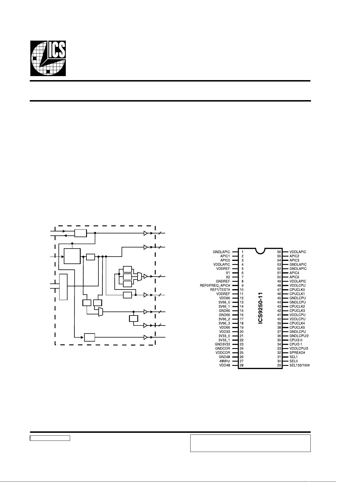
Block Diagram
Frequency Timing Generator for PENTIUM II/III Systems
9250-11 Rev C 3/20/00
Pin Configuration
56-pin SSOP
Generates the following system clocks:
- 6 - CPU Clocks 100/133MHz (2.5V).
- 2 - CPU/2 output for synchronous memory
reference (2.5V).
- 4 - fixed frequency Clocks @ 66.6MHz (3.3V).
- 2 - fixed frequency Clocks @ 33.3MHz (3.3V).
- 6 - IOAPIC Clocks @ ¼ of CPUCLK or 16.667MHz,
synchronous to CPU Clock (2.5V)
- 1 - 48MHz Clock (3.3V)
- 2 - REF Clocks @ 14.31818MHz
0.5% typical down spread modulation on CPU, PCI,
IOAPIC, 3V66 and CPU/2 output clocks.
Uses external 14.318MHz crystal.
The ICS9250-11 is a main clock synthesizer chip for Pentium
II based systems using Rambus Interface DRAMs. This chip
provides all the clocks required for such a system when used
with a Direct Rambus Clock Generator (DRCG) chip such as
the ICS9212-01, 02, 03 and a PCI buffer 9112-17.
Spread Spectrum may be enabled by driving the SPREAD#
pin active. Spread spectrum typically reduces system EMI by
8dB to 10dB. This simplifies EMI qualification without
resorting to board design iterations or costly shielding. The
ICS9250-11 employs a proprietary closed loop design, which
tightly controls the percentage of spreading over process and
temperature variations.
The CPU/2 clocks are inputs to the DRCG.
SEL 133/100#
SEL(0:1)
SPREAD#
X1
X2
OSC
PLL
Spread
Spectrum
PLL2
CPU/2 (0:1)
REF (0:1)
2
6
4
2
2
CPUCLK (0:5)
3V66 (0:3)
48MHz
/ 2
/ 3 / 2
3V33 (0:1)
C
o
n
t
r
o
l
/ 2
/ 2
/ 4
/ 3
/ 2
IOAPIC(0:5)
6
Power Groups:
VDDREF, GNDREF = REF, X1, X2
VDD66, GND66 = 3V66
VDD33, GND33 = 3V33
VDD48, GND48 = 48MHz
VDDCOR, GNDCOR = PLL Core
VDDLCPU, GNDLCPU = CPUCLK
VDDLCPU/2 , GNDLCPU/2 = CPU/2
VDDLAPIC, GNDAPIC = IOAPIC
ICS reserves the right to make changes in the device data identified in this
publication without further notice. ICS advises its customers to obtain the
latest version of all device data to verify that any information being relied
upon by the customer is current and accurate.
Page 2
2
ICS9250-11
Pin Descriptions
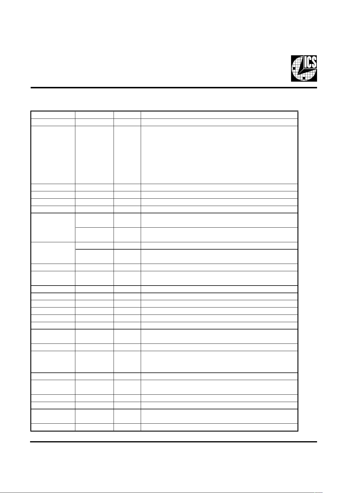
Pin number Pin name Type Description
1, 52, 53 GNDLAPIC PWR Ground pin for the IOA PIC outputs.
2, 3, 50, 51, 54, 55 IOAP IC ( 0: 5) OUT
2.5V clock outputs run ning di vi de synchronous w it h t h e C PU
(Host bus) clock f requency. The default API C is r unni ng at ¼ of
CP UCLK frequenc y .
When FREQ _APIC is strapped low, the APIC is running at fixed
16.67 M Hz.
If CPU = 133 MHz, APIC = CPU/8
If CPU = 100 MHz, APIC = CPU/6
4, 49, 56 VDDLAPIC PWR Power pin for the IOAPI C out put s. 2.5V.
5, 11 V DDREF PWR Power pin for REF clocks
6 X1 IN X TA L_IN 14.318MHz cryst a l i nput
7 X2 OUT XTAL_O UT Crystal out pu t
REF0 OUT
3.3V 14.318 MHz clock output. APIC cloc k strapping option for
fi xe d 16.67 MHz APIC c l ock outputs.
FREQ_APIC# OUT
If FREQ_APIC# = 0, APIC Cloc k = 16.67 MHz
If FREQ_AP IC# = O pen, AP IC Clock = CPU/4
REF1 OUT 3.3V 1 4.318MHz c lock output.
TEST# OUT
TE ST# is sa mpled lo w (external wi th 10 k pu l ldown). All cl ock
outputs are Tri -St a te .
12, 19 VDD66 PWR pow e r pin for the 3V66 clocks.
13, 14, 17, 18 3V 66[0:3] OUT
66MH z output s a t 3.3V . These outputs ar e s t oppe d when
CPU_ST OP# is driven ac tive ..
8, 15, 16, 23, 2 4 G ND PWR Ground pin for 3V outputs.
21, 22 3V 33MHz OUT 3.3V F i xe d 33MHz clock outpu t .
25 VDDCOR PWR 3.3V power for PLL core.
26 GND48 PWR Ground pin for the 48MHz output
27 48MH z OUT Fixed 48MHz clock out p ut. 3.3V
28 VDD48 PWR Power pin for the 48MHz output .
29 S EL 133/100# IN
This sel ects t he freque nc y for the CPU and CPU/ 2 out p ut s. High =
133MH z, Low=100MHz
30, 31 SEL[0:1] I N Function select pi n s. See t ruth table for details.
32 SPREAD# IN
Enables spr e ad s pectrum when active(Low). modulates all the CP U,
PC I, IOAP IC, 3V 66 a n d C PU/2 clocks. Does not a ffect t he REF and
48MH z c l ocks. 0.5% down spread mo dul ation.
33 VDDLCPU/2 PWR Power pin for the CPU/2 clocks. 2.5V
34, 35 CPU/2[ 0: 1] OUT
2.5V clock outputs at 1/2 C PU frequency. 66MHz or50MHz
dependi ng on t he stat e of the SEL 133/100# input pi n.
36 GNDLCPU/2 PWR Ground pin for the CPU/2 clocks .
37, 4 4, 45 GNDLCP U PWR Ground pi n for the C PUCLKs
38, 39, 42, 43, 46,
47
CPUCLK[0:5] OUT
Ho st bus clock output at 2.5 V. 133MH z or 100MHz depending on
the st a te of the S E L 133/100MHz.
40, 41, 48 VD DLCP U PWR Pow er pin for the CP UCLKs. 2.5V
9
10
Page 3
3
ICS9250-11
Frequency Select:
Power Management Features:
LES
#001/331
1LES0LES
UPC
zHM
2/UPC
zHM
66V3
zHM
33V3
zHM
84
zHM
FER
zHM
zHMCIPAOI
000 etatsirTetatsirTetatsirTetatsirTetatsirTetatsirTetatsirT
001A/NA/NA/NA/NA/NA/NA/N
010 00100.056.663.33FFO813.4176.61/KLCUPC¼
011 00100.056.663.3384813.4176.61/KLCUPC¼
100 2/KLCT4/KLCT4/KLCT8/KLCT2/KLCTKLCT61/KLCT
101 A/NA/NA/NA/NANA/NA/N
110 3.3316.666.663.33FFO813.4176.61/KLCUPC¼
111 3.3316.666.663.3384813.4176.61/KLCUPC¼
#001/331LES1LES0LESnoitcnuF
00 0 etatS-irTstuptuollA
0001devreseR
01 0 evitcaniLLPzHM84,zHM001evitcA
01 1 evitcaLLPzHM84,zHM001evitcA
10 0 edoMtseT
10 1 devreseR
11 0 evitcaniLLPzHM84,zHM331evitcA
11 1 evitcaLLPzHM84,zHM331evitcA
Page 4

4
ICS9250-11
Absolute Maximum Ratings
Supply Voltage. . . . . . . . . . . . . . . . . . . . . . . . . . . 7.0 V
Logic Inputs. . . . . . . . . . . . . . . . . . . . . . . . . . . . . GND 0.5 V to VDD +0.5 V
Ambient Operating Temperature . . . . . . . . . . . . 0°C to +70°C
Storage Temperature . . . . . . . . . . . . . . . . . . . . . . 65°C to +150°C
Stresses above those listed under Absolute Maximum Ratings may cause permanent damage to the device. These ratings are stress
specifications only and functional operation of the device at these or any other conditions above those listed in the operational
sections of the specifications is not implied. Exposure to absolute maximum rating conditions for extended periods may affect
product reliability.
Electrical Characteri stics - Input/Supply/Common Output Paramete rs
TA = 0 - 70C; Supply Voltage VDD = 3.3 V +/-5%, V
DDL
= 2.5 V +/-5% (unless otherwise stated)
PARAMETER SYMBOL CONDITIONS MIN TYP MAX UNITS
Inpu t High Vol t age V
IH
2V
DD
+0.3 V
In put Low Voltage V
IL
VSS-0.3 0.8 V
Input High C urrent I
IH
VIN = V
DD
5
µ
A
I
IL1
VIN = 0 V; I nput s with no pull-up resistor s -5
I
IL2
VIN = 0 V; I nput s with pull-up resistors 20 0
C
L
= Ma x loa ds ; Selec t @ 100 MH z 160
C
L
= Ma x loa ds ; Selec t @ 133 MH z 160
C
L
= Ma x loa ds ; Selec t @ 100 MH z 75
C
L
= Ma x loa ds ; Selec t @ 133 MH z 90
I
DD3.3PD
CL = Max loads
200
I
DD.25PD
In put addre ss VDD or GND
100
Input F requency F
i
VDD = 3.3 V 14.318 MHz
Pin Inducta nc e
1
L
pin
7nH
C
IN
Logic Inputs 5 pF
C
OUT
O utp ut pin capacitance 6 pF
C
INX
X 1 & X 2 pins 1 3.5 1 8 2 2.5 pF
Tr ansition time
1
T
trans
To 1st crossing of target fr e q ue n c y 3 ms
Clk Stabilization
1
T
STAB
From VDD = 3.3 V to 1% target frequency 3 ms
t
PZH,tPZL
O utput e nab le del ay (all outputs) 1 8 ns
t
PHZ,tPLZ
O utp ut disable del a y (all outputs) 1 8 ns
T
CPU-3V66
CPU @ 1.25V, 3V66 @ 1.5V 0 1.5 ns
T
3V66-3V33
3V66 @ 1.5V, 3V 33 @ 1.5V 1.5 3.5 ns
T
CPU-IOAPIC
CPU @ 1.25V , IOAPIC @ 1.25V 1.0 3.0 ns
1
Guara nteed by design, n ot 100% te sted in product ion.
Input Low Current
µ
A
I
DD3.3OP
Delay
1
mA
Inpu t Capacitance
1
I
DD.25OP
µ
APowerdown Current
O perat i ng Supply
Current
mA
Skew
1
Page 5

5
ICS9250-11
Ele ctrical Characteristic s - CPU
TA = 0 - 70C; V
DDL
= 2.5 V +/-5%; CL = 10-2 0 pF ( u nless otherwise specified)
PARAMETER SYMBOL CONDITIONS MIN TYP MAX UNITS
O utput High Vol ta ge V
OH2BIOH
= -12 mA 2 V
Output Low Voltage V
OL2BIOL
= 12 mA 0.4 V
V
OH @ MIN
= 1.0 V -27
V
OH @ MAX
= 2.375 V -27
V
OL @ MIN
= 1.2 V 27
V
OL @ MAX
= 0.3 V 30
Rise Time
1
t
r2B
VOL = 0.4 V, VOH = 2.0 V 0.4 1.6 ns
Fall Time
1
t
f2B
VOH = 2.0 V , VOL = 0.4 V 0.4 1.6 ns
Duty Cycle
1
d
t2B
VT = 1.25 V 45 55 %
Skew window
1
t
sk2B
VT = 1.25 V 175 ps
Jitter, cycle-to-cycle
1
t
jcyc-cyc2BVT
= 1.25 V
150 ps
1
Guara nteed by design, no t 100% tested in product ion.
mA
mA
Ou tput High Curr ent
Output Low Current
I
OH2B
I
OL2B
Ele ctrical Characteristics - CPU/2
TA = 0 - 70C; V
DDL
= 2.5 V +/-5%; CL = 10-2 0 pF ( u nless otherwise specified)
PARAMETER SYMBOL CONDITIONS MIN TYP MAX UNITS
O utput High Vol ta ge V
OH2BIOH
= -12 mA 2 V
Output Low Voltage V
OL2BIOL
= 12 mA 0.4 V
V
OH @ MIN
= 1.0 V -27
V
OH @ MAX
= 2.375 V -27
V
OL @ MIN
= 1.2 V 27
V
OL @ MAX
= 0.3 V 30
Rise Time
1
t
r2B
VOL = 0.4 V, VOH = 2.0 V 0.4 1.6 ns
Fall Time
1
t
f2B
VOH = 2.0 V , VOL = 0.4 V 0.4 1.6 ns
Duty Cycle
1
d
t2B
VT = 1.25 V 45 55 %
Skew window
1
t
sk2B
VT = 1.25 V 175 ps
Jitter, cycle-to-cycle
1
t
jcyc-cyc2BVT
= 1.25 V
250 ps
1
Guara nteed by design, no t 100% tested in produc tion.
mA
mA
Ou tput High Curr ent
Output Low Current
I
OH2B
I
OL2B
Page 6

6
ICS9250-11
Ele ctrical Characteristic s - 3V33
TA = 0 - 70C; VDD = 3.3 V +/-5%; CL = 10-30 pF (unless otherwise specified)
PARAMETER SYMBOL CONDITIONS MIN TYP MAX UNITS
O utput High Vol ta ge V
OH1
IOH = -14.5 mA 2.4 V
Output Low Voltage V
OL1
IOL = 9.4 mA 0.4 V
V
OH @ MIN
= 1.0 V -33
V
OH @ MAX
= 3.135 V -33
V
OL @ MIN
= 1.95 V 30
V
OL @ MAX
= 0.4 V 38
Rise Time
1
t
r1
VOL = 0.4 V, VOH = 2.4 V 0.5 2.0 ns
Fall Time
1
t
f1
VOH = 2.4 V , VOL = 0.4 V 0.5 2.0 ns
Duty Cycle
1
d
t1
VT = 1.5 V 45 55 %
Skew window
1
t
sk1
VT = 1.5 V 250 ps
Jitter, cycle-to-cycle
1
t
jcyc-cyc1
VT = 1.5 V
250 ps
1
Guara nteed by design, no t 100% tested in product ion.
Ou tput High Curr ent
Output Low Current
mA
mA
I
OH1
I
OL1
Ele ctrical Characteristic s - 3V66
TA = 0 - 70C; VDD = 3.3 V +/-5%; CL = 10-30 pF (unless otherwise specified)
PARAMETER SYMBOL CONDITIONS MIN TYP MAX UNITS
O utput High Vol ta ge V
OH1
IOH = -14.5 mA 2.4 V
Output Low Voltage V
OL1
IOL =9 mA 0.4 V
V
OH @ MIN
= 1.0 V -33
V
OH @ MAX
= 3.135 V -33
V
OL @ MIN
= 1.95 V 30
V
OL @ MAX
= 0.4 V 38
Rise Time
1
t
r1
VOL = 0.4 V, VOH = 2.4 V 0.5 2.0 ns
Fall Time
1
t
f1
VOH = 2.4 V , VOL = 0.4 V 0.5 2.0 ns
Duty Cycle
1
d
t1
VT = 1.5 V 45 55 %
Skew window
1
t
sk1
VT = 1.5 V 250 ps
Jitter, cycle-to-cycle
1
t
jcyc-cyc1VT
= 1.5 V
500 ps
1
Guara nteed by design, no t 100% tested in product ion.
Ou tput High Curr ent
Output Low Current
mA
mA
I
OH1
I
OL1
Page 7

7
ICS9250-11
Ele ctrical Charact eristics - REF, 48MHz
TA = 0 - 70C; VDD = 3.3 V +/-5%; CL = 10-20 pF (unless otherwise specified)
PARAMETER SYMBOL CONDITIONS MIN TYP MAX UNITS
O utput High Vol ta ge V
OH5
IOH = -16 mA 2.4 V
Output Low Voltage V
OL5
IOL = 9 mA 0.4 V
V
OH @ MIN
= 1.0 V -29
V
OH @ MAX
= 3.135 V -23
V
OL @ MIN
= 1.95 V 29
V
OL @ MAX
= 0.4 V 27
Rise Time
1
t
r5
VOL = 0.4 V, VOH = 2.4 V 1.0 4.0 ns
Fall Time
1
t
f5
VOH = 2.4 V , VOL = 0.4 V 1.0 4.0 ns
Duty Cycle
1
d
t5
VT = 1.5 V 45 55 %
Jitter, cycle-to-cycle
1
t
jcyc-cyc5
VT = 1.5 V, Fixed clocks 500 ps
Jitter, cycle-to-cycle
1
t
jcyc-cyc5
VT = 1.5 V, Ref clocks
1000 ps
1
Guara nteed by design, no t 100% tested in produc tion.
Ou tput High Curr ent I
OH5
mA
Output Low Current I
OL5
mA
Electrical Characteristics - IOAPIC
TA = 0 - 70C; V
DDL
= 2.5 V +/-5%; CL = 10-2 0 pF ( u nless otherwise specified)
PARAMETER SYMBOL CONDITIONS MIN TYP MAX UNITS
O utput High Vol ta ge V
OH2BIOH
= -12 mA 2 V
Output Low Voltage V
OL2BIOL
= 12 mA 0.4 V
V
OH @ MIN
= 1.0 V -27
V
OH @ MAX
= 2.375 V -27
V
OL @ MIN
= 1.2 V 27
V
OL @ MAX
= 0.3 V 30
Rise Time
1
t
r2B
VOL = 0.4 V, VOH = 2.0 V 0.4 1.6 ns
Fall Time
1
t
f2B
VOH = 2.0 V , VOL = 0.4 V 0.4 1.6 ns
Duty Cycle
1
d
t2B
VT = 1.25 V 45 55 %
Skew window
1
t
sk2B
VT = 1.25 V 250 ps
Jitter, cycle-to-cycle
1
t
jcyc-cyc2BVT
= 1.25 V
250 ps
1
Guara nteed by design, no t 100% tested in product ion.
mA
mA
Ou tput High Curr ent
Output Low Current
I
OH2B
I
OL2B
Page 8

8
ICS9250-11
ICS reserves the right to make changes in the device data identified in this
publication without further notice. ICS advises its customers to obtain the
latest version of all device data to verify that any information being relied
upon by the customer is current and accurate.
LOBMYSSNOISNEMIDNOMMOCSNOITAIRAVDN
.NIM.MON.XAM.NIM.MON.XAM
A590.201.011.DA027.527.037.65
1A800.210.610.
2A780.090.490.
B800.- 5310.
c500.-010.
DsnoitairaVeeS
E192.592.992.
eCSB520.0
H593.-024.
h010.310.610.
L020.-040.
NsnoitairaVeeS
µ
°0- °8
56 Pin 300 mil SSOP Package
“For current dimensional specifications, see JEDEC 95.”
.093
DIA. PIN (Optional)
D/2
E/2
BOTTOM VIEW
A
2
SEE
DETAIL “A”
-E-
c
END VIEW
H
Pin 1
TOP VIEW
Index
Area
PARTING LINE
L
DETAIL “A”
A
1
-e-
B
A
SIDE VIEW
-C-
-D-
SEATING
PLANE
.004
C
Ordering Information
ICS9250yF-11-T
Designation for tape and reel packaging
Pattern Number (2 or 3 digit number for parts with ROM code patterns)
Package Type
F=SSOP
Revision Designator (will not correlate with datasheet revision)
Device Type (consists of 3 or 4 digit numbers)
Prefix
ICS, AV = Standard Device
Example:
ICS XXXX y F - PPP - T
Dimensions in inches
 Loading...