

Integrated
Circuit
Systems, Inc.
General Description Features
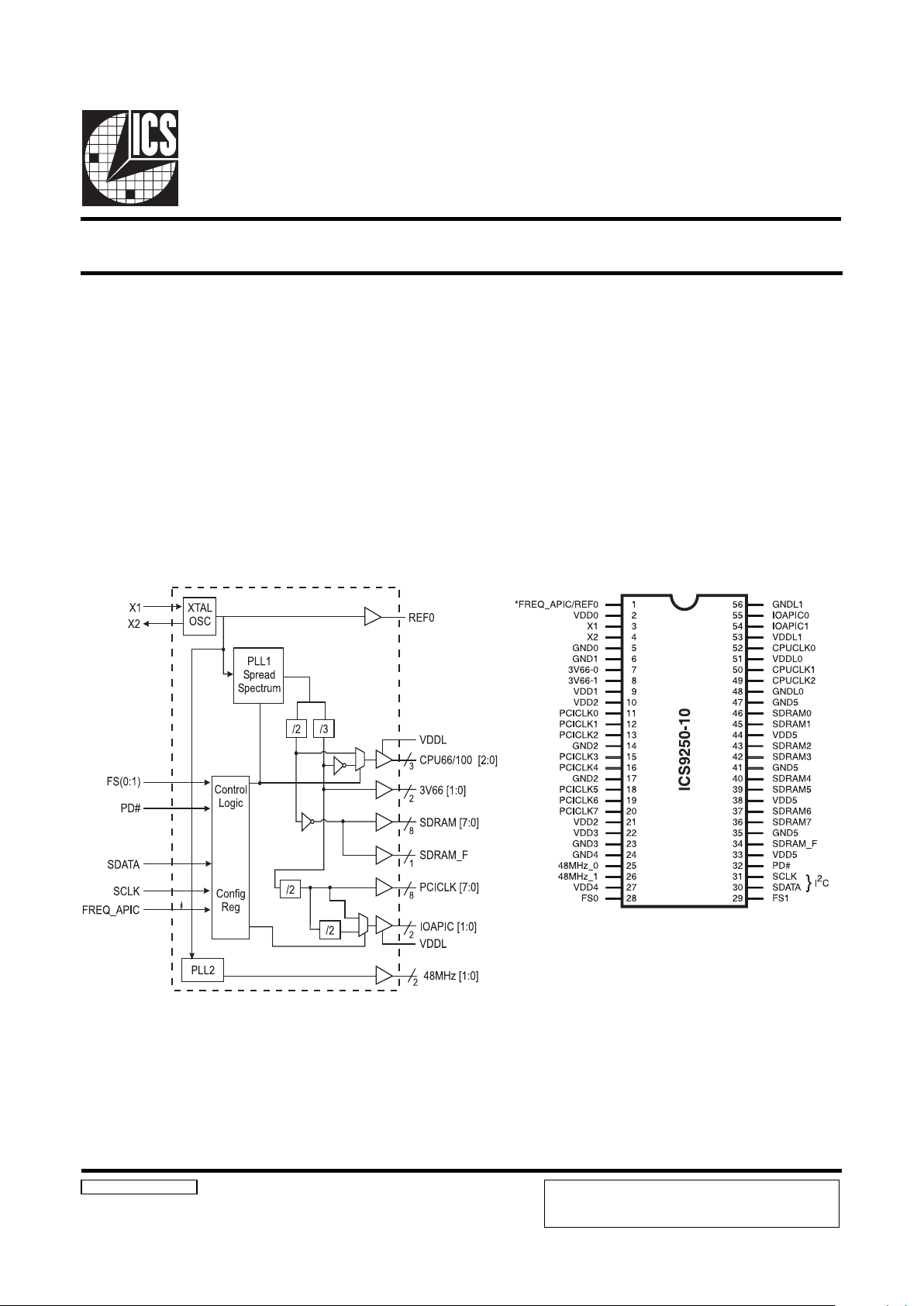
ICS9250-10
PRODUCT PREVIEW documents contain information on new
products in the sampling or preproduction phase of development.
Characteristic data and other specifications are subject to change
without notice.
Preliminary Product Preview
Block Diagram
Pentium II is a trademark of Intel Corporation
I2C is a trademark of Philips Corporation
Frequency Timing Generator for Pentium II Systems
9250-10 Rev J 6/15/99
Pin Configuration
Generates the following system clocks:
- 3 CPU (2.5V) 66.6/100 MHz (up to 133MHz through
I2C selection)
- 9 SDRAM (3.3V) up to 133MHz
- 8 PCI (3.3 V) @33.3MHz
- 2 IOAPIC (2.5V) @16.67 or 33.3MHz
- 2 Hublink clocks (3.3 V) @ 66.6 MHz
- 2 USB (3.3V) @ 48 MHz ( Non spread spectrum)
- 1 REF (3.3V) @ 14.318 MHz
Supports spread spectrum modulation ,
down spread 0 to -0.5%
I2C support for power management
Efficient power management scheme through PD#
Uses external 14.138 MHz crystal
56-Pin 300 mil SSOP
The ICS9250-10 is a single chip clock for Intel Pentium II.
It provides all necessary clock signals for such a system.
Spread spectrum may be enabled through I2C programming.
Spread spectrum typically reduces EMI by 8dB to 10 dB.
This simplifies EMI qualification without resorting to board
design iterations or costly shielding. The ICS9250-10
employs a proprietary closed loop design, which tightly
controls the percentage of spreading over process and
temperature variations.
Power Groups
VDD0, GND0 = REF & Crystal
VDD1, GND1 = 3V66 [1:0]
VDD2, GND2 = PCICLK[7:0]
VDD3, GND3 = PLL core
VDD4, GND4 = 48MHz [1:0]
VDD5, GND5 = SDRAM_F, SDRAM [7:0]
VDDL0, GNDL0 = CPUCLK [2:0]
VDDL1, GNDL1 = IOAPIC [1:0]
*60K ohm pull-up to VDD on indicated inputs.
2
ICS9250-10
Preliminary Product Preview
Pin Descriptions
REBMUNNIPEMANNIPEPYTNOITPIRCSED
1
CIPA_QERFNI
.ycneuqerfCIPAOIehtsenimretedsiht.nOrewoPtatupnidehctaL
zHM76.61=qerFCIPAOI,dehctalsi"0"anehW
zHM3.33=qerFCIPAOI,dehctalsi"1"nehW
.pu-lluplanretniK06asahnipsihT
0FERTUO.tuptuokcolcecnereferzHM813.41,V3.3
31XNI
kcabdeefdna)Fp33(pacdaollanretnisah,tupnilatsyrC
2Xmorfrotsiser
42XTUO
daollanretnisaH.zHM813.41yllanimon,tuptuolatsyrC
)Fp33(pac
,32,71,41,6,5
74,14,53,42
)5:0(DNGRWPylppusV3.3rofsnipdnuorG
7,8]0:1[66V3TUOBUHrofstuptuokcolczHM66dexiFV3.3
,12,01,9,2
44,83,33,72,22
)5:0(DDVRWPylppusrewopV3.3
,61,81,91,02
11,21,31,51
]0:7[KLCICPTUOSKLCUPCsuonorhcnyShtiw,stuptuokcolcICPV3.3
62,52)1:0(zHM84TUOBSUrofstuptuokcolczHM84dexiFV3.3
92,82)1:0(SFNI
tuptuolla,ycneuqerfUPCsenimreteD.sniptceleSnoitcnuF
.3egapnoelbatytilanoitcnuFotreferesaelP.ytilanoitcnuf
03ATADSNIIroftupniataD
2
.tupnilairesC
13KLCSNIIfotupnikcolC
2
tupniC
23#DPNI
ecivedehtnwodrewopotdesuniptupniwolevitcasuonorhcnysA
ehtdnadelbasideraskcolclanretniehT.etatsrewopwolaotni
nwodrewopehtfoycnetalehT.deppotseralatsyrcehtdnaOCV
.sm3nahtretaergebtonlliw
,24,04,93,73,63
64,54,34
]0:7[MARDSTUO
denrutebnacstuptuoMARDSllA.zHM001gninnurtuptuoV3.3
Ihguorhtffo
2
C
43F_MARDSTUOIybdetceffatonMARDSzHM001gninnureerfV3.3
2
C
84,65]0:1[LDNGRWPCIPA&UPCrofylppusrewopV5.2rofdnuorG
25,05,94]0:2[KLCUPCTUO
SFnognidnepedzHM001rozHM66.tuptuokcolcsubtsoHV5.2
.3egaprefeRsnip)1:0(
35,15)1:0(LDDVRWPCIPAOI&UPCrofylppyusrewopV5.2
55,45]0:1[CIPAOITUO.zHM3.33rozHM76.61tagninnurstuptuokcolcV5.2
3
ICS9250-10
Preliminary Product Preview
Functionality Table
1SF0SFUPCMARDS66V3KLCICPzHM840FERCIPAOIsetoN
00 Z-iHZ-iHZ-iHZ-iHZ-iHZ-iHZ-iHetatsirT
01 2/KLCT4/KLCT4/KLCT8/KLCT2/KLCTKLCT61/KLCTedoMtseT
10 zHM66zHM001zHM66zHM33zHM84zHM813.41zHM76.61
11 zHM001zHM001zHM66zHM33zHM84ZHM813.41zHM76.61
Select Functions
#DPKLCUPCMARDSCIPAOIzHM66KLCICP
,FER
zHM84
csOsOCV
0WOLWOLWOLWOLWOLWOLFFOFFO
1NONONONONONONONO
1SF0SFsetoN
00 etatsirT
01 edoMtseT
10 zHM66=UPCevitcA
11 zHM001=UPCevitcA
Clock Enable Configuration
4
ICS9250-10
Preliminary Product Preview
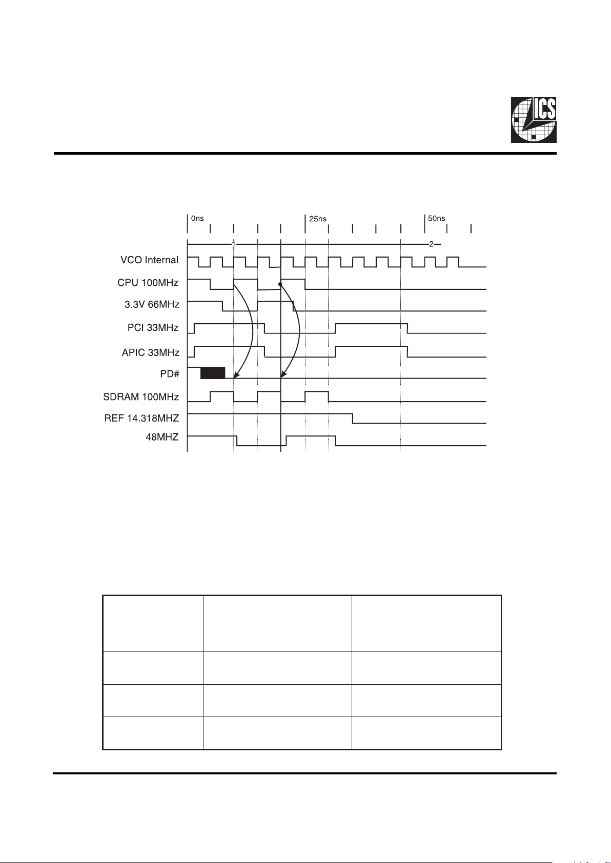
Power Down Waveform
Note
1. After PD# is sampled active (Low) for 2 consective rising edges of CPUCLKs, all
the output clocks are driven Low on their next High to Low tranistiion.
2. Power-up latency <3ms.
3. Waveform shown for 100MHz
E018
noitidnoC
noitpmusnocylppusV5.2xaM
,sdaolpacetercsidxaM
V526.2=2qddV
DNGro3qddV=stupnicitatsllA
noitpmusnocylppusV5.2xaM
,sdaolpacetercsidxaM
V564.3=2qddV
DNGro3qddV=stupnicitatsllA
edoMnwodrewoP
0=#NWDRWP(
Am01Am01
zHM66evitcAlluF
01=0,1LES
Am07Am082
zHM001evitcAlluF
11=0,1LES
Am001Am082
Maximum Allowed Current
5
ICS9250-10
Preliminary Product Preview
1. The ICS clock generator is a slave/receiver, I2C component. It can read back the data stored in the latches for verification.
Read-Back will support Intel PIIX4 "Block-Read" protocol.
2. The data transfer rate supported by this clock generator is 100K bits/sec or less (standard mode)
3. The input is operating at 3.3V logic levels.
4. The data byte format is 8 bit bytes.
5. To simplify the clock generator I2C interface, the protocol is set to use only "Block-Writes" from the controller. The
bytes must be accessed in sequential order from lowest to highest byte with the ability to stop after any complete byte
has been transferred. The Command code and Byte count shown above must be sent, but the data is ignored for those
two bytes. The data is loaded until a Stop sequence is issued.
6. At power-on, all registers are set to a default condition, as shown.
General I2C serial interface information
The information in this section assumes familiarity with I2C programming.
For more information, contact ICS for an I2C programming application note.
How to Write:
Controller (host) sends a start bit.
Controller (host) sends the write address D2
(H)
ICS clock will acknowledge
Controller (host) sends a dummy command code
ICS clock will acknowledge
Controller (host) sends a dummy byte count
ICS clock will acknowledge
Controller (host) starts sending first byte (Byte 0)
through byte 5
ICS clock will acknowledge each byte one at a time.
Controller (host) sends a Stop bit
How to Read:
Controller (host) will send start bit.
Controler (host) sends the read address D3
(H)
ICS clock will acknowledge
ICS clock will send the byte count
Controller (host) acknowledges
ICS clock sends first byte (Byte 0) through byte 5
Controller (host) will need to acknowledge each byte
Controller (host) will send a stop bit
Notes:
Controller (Host) ICS (Slave/Receiver)
Start Bit
Address
D3
(H)
AC
K
Byte Count
ACK
Byte
0
ACK
Byte 1
ACK
Byte
2
ACK
Byte
3
ACK
Byte 4
ACK
Byte
5
ACK
Stop Bit
How to Read:
Controller (Host) ICS (Slave/Receiver)
Start Bit
Address
D2
(H)
AC
K
Dummy Command Code
AC
K
Dummy Byte Count
AC
K
Byte 0
AC
K
Byte 1
ACK
Byte 2
AC
K
Byte 3
AC
K
Byte 4
AC
K
Byte 5
AC
K
Stop Bit
How to Write:

6
ICS9250-10
Preliminary Product Preview
tiBnoitpitcseDDWP
7tiB )lamronetarepootkcolc0ebotsdeeN(TIBDEVRESERSCI0
6tiB )lamronetarepootkcolc0ebotsdeeN(TIBDEVRESERSCI0
5tiB )lamronetarepootkcolc0ebotsdeeN(TIBDEVRESERSCI0
tiB
)0,3,4(
)0,3,4(tiB
KLCUPC
zHM
MARDS
zHM
66V3
zHM
KLCICP
zHM
XXXX
1etoN
0SF
)WH(
3LES
)4tiB(
2LES
)3tiB(
1LES
)0tiB(
0000 76.6600176.6633.33
0001 76.0760176.0733.53
0010 66.4721176.4733.73
0011 66.2842166.2833.14
0100 5.3652.595.3657.13
0101 76.8630176.8633.43
0110 76.2790176.2733.63
0111 66.8833166.8833.44
1000 00100176.6633.33
1001 60160176.0733.53
1010 21121176.4733.73
1011 42142166.2833.14
1100 52.5952.595.3657.13
1101 30130176.8633.43
1110 90190176.2733.63
1111 33133166.8833.44
2tiB)noitarepokcolclamronrof1ebotsdeeN(desutoN 1
1tiB)noitarepokcolclamronrof1ebotsdeeN(desutoN 1
Byte 5:ICS Reserved Functionality and frequency select register (Default=0)
Note1: Default at power-up will be for latched logic inputs to define frequency, as diplayed by Bit 3.

7
ICS9250-10
Preliminary Product Preview
Byte 0: Control Register
(1 = enable, 0 = disable)
Byte 1: Control Register
(1 = enable, 0 = disable)
Byte 2: Control Register
(1 = enable, 0 = disable)
Notes:
1. Inactive means outputs are held LOW and are disabled from switching. These outputs are designed to be configured
at power-on and are not expected to be configured during the normal modes of operation.
2. PWD = Power on Default
tiB#niPemaNDWPnoitpircseD
7tiBdevreseR0)evitcanI/evitcA(
6tiBdevreseR0)evitcanI/evitcA(
5tiBdevreseR0)evitcanI/evitcA(
4tiBdevreseR1)evitcanI/evitcA(
3tiB
murtcepSdaerpS
)ffO=0/nO=1(
1)evitcanI/evitcA(
2tiB621zHM841)evitcanI/evitcA(
1tiB520zHM841)evitcanI/evitcA(
0tiB942KLCUPC1)evitcanI/evitcA(
tiB#niPemaNDWPnoitpircseD
7tiB637MARDS1)evitcanI/evitcA(
6tiB736MARDS1)evitcanI/evitcA(
5tiB935MARDS1)evitcanI/evitcA(
4tiB044MARDS1)evitcanI/evitcA(
3tiB243MARDS1)evitcanI/evitcA(
2tiB342MARDS1)evitcanI/evitcA(
1tiB541MARDS1)evitcanI/evitcA(
0tiB640MARDS1)evitcanI/evitcA(
tiB#niPemaNDWPnoitpircseD
7tiB027KLCICP1)evitcanI/evitcA(
6tiB916KLCICP1)evitcanI/evitcA(
5tiB815KLCICP1)evitcanI/evitcA(
4tiB614KLCICP1)evitcanI/evitcA(
3tiB513KLCICP1)evitcanI/evitcA(
2tiB312KLCICP1)evitcanI/evitcA(
1tiB211KLCICP1)evitcanI/evitcA(
0tiB- devreseR0)evitcanI/evitcA(

8
ICS9250-10
Preliminary Product Preview
Byte 3: Reserved Register
(1 = enable, 0 = disable)
Byte 4: Reserved Register
(1 = enable, 0 = disable)
tiB#niPemaNDWPnoitpircseD
7tiB- devreseR0)evitcanI/evitcA(
6tiB- devreseR0)evitcanI/evitcA(
5tiB- devreseR0)evitcanI/evitcA(
4tiB- devreseR0)evitcanI/evitcA(
3tiB- devreseR0)evitcanI/evitcA(
2tiB- devreseR0)evitcanI/evitcA(
1tiB- devreseR0)evitcanI/evitcA(
0tiB- devreseR0)evitcanI/evitcA(
tiB#niPemaNDWPnoitpircseD
7tiB- devreseR0)evitcanI/evitcA(
6tiB- devreseR0)evitcanI/evitcA(
5tiB- devreseR0)evitcanI/evitcA(
4tiB- devreseR0)evitcanI/evitcA(
3tiB- devreseR0)evitcanI/evitcA(
2tiB- devreseR0)evitcanI/evitcA(
1tiB- devreseR0)evitcanI/evitcA(
0tiB- devreseR0)evitcanI/evitcA(
Notes:
1. Inactive means outputs are held LOW and are disabled from switching. These outputs are designed to be configured
at power-on and are not expected to be configured during the normal modes of operation.
2. PWD = Power on Default

9
ICS9250-10
Preliminary Product Preview
Absolute Maximum Ratings
Core Supply Voltage . . . . . . . . . . . . . . . . . . . . . . 4.6 V
I/O Supply Voltage . . . . . . . . . . . . . . . . . . . . . . . 3.6V
Logic Inputs . . . . . . . . . . . . . . . . . . . . . . . . . . . . GND 0.5 V to VDD +0.5 V
Ambient Operating Temperature . . . . . . . . . . . . 0°C to +70°C
Storage Temperature . . . . . . . . . . . . . . . . . . . . . . 65°C to +150°C
Stresses above those listed under Absolute Maximum Ratings may cause permanent damage to the device. These ratings are
stress specifications only and functional operation of the device at these or any other conditions above those listed in the
operational sections of the specifications is not implied. Exposure to absolute maximum rating conditions for extended
periods may affect product reliability.
Electrical Characteristics - Input/Supply/Common Output Parameters
TA = 0 - 70C; S upply Voltage VDD = 3.3 V +5%, VDDL=2.5 V+ 5%(unless ot he rwise sta t e d)
PARAMETER SYMBOL CONDITIONS MIN TYP MAX UNITS
Input High V oltage V
IH
2V
DD
+0.3 V
Input L ow Voltage V
IL
VSS-0.3 0.8 V
Inpu t High Cur rent I
IH
VIN = V
DD
-5 5
µ
A
Input Low Current I
IL1
VIN = 0 V; Inputs with no pull-u p resist ors -5 2.0
µ
A
Input Low Current I
IL2
VIN = 0 V; Inputs with pull-up resis to rs -200 -100
µ
A
Operating I
DD3.3OP
CL = 0 pF; Selec t @ 66M 60 100 m A
Suppl y C urrent
Power Down I
DD3.3PD
CL = 0 pF; With input a ddress to Vdd or GND 400 600
µ
A
Suppl y C urrent
Input f requency F
i
VDD = 3.3 V; 14.318 MHz
Pin Inductance L
pin
7nH
Input Capa c itanc e
1
C
IN
Logic Inputs 5 pF
C
out
O ut p ut pin c a pa c i ta nce 6 pF
C
INX
X 1 & X2 pins 27 45 pF
Tr a ns ition T ime
1
T
trans
To 1st crossing of target Freq. 3 mS
Se ttling Tim e
1
T
s
From 1st c rossing to 1% target Freq. 3 mS
Clk S tabiliz a tion
1
T
STAB
From VDD = 3.3 V to 1% ta rget Freq. 3 mS
Delay t
PZH,tPZH
output ena ble de la y (all outputs ) 1 10 nS
t
PLZ,tPZH
output dis a bl e de l ay (all outputs) 1 10 nS
1
G ua renteed by design, not 100% te sted in production.

10
ICS9250-10
Preliminary Product Preview
Electrical Characteristics - 3V66
TA = 0 - 70C; VDD = 3.3 V + /-5%; CL = 1 0-30 pF (u nless oth erwis e stated)
PARA METER SY MBOL CON DI TION S MIN TYP MAX UN ITS
O utput Impedanc e R
DSP1
1
VO = VDD*(0.5) 12 55
Ω
O utput Impedanc e R
DSN1
1
VO = VDD*(0.5) 12 55
Ω
O utput High Volta ge V
OH1
IOH = -1 mA 2.4 V
O utput L ow Voltage V
OL1
IOL = 1 mA 0.55 V
O utput High Curr e nt I
OH1
VOH@ MIN = 1.0 V, VOH@ MAX = 3.135 V-33 -33 mA
O utput L o w Current I
OL1
VOL@ MIN = 1.95 V, VOL@ MAX= 0.4 30 38 mA
Rise Time t
r1
1
VOL = 0. 4 V, VOH = 2.4 V 0.5 2 ns
Fall Time t
f1
1
VOH = 2.4 V, VOL = 0.4 V 0.5 2 ns
Duty Cycle d
t1
1
VT = 1.5 V 45 55 %
Skew t
sk1
1
VT = 1.5 V 175 ps
Jitte r t
jcyc-cyc
VT = 1.5 V 500 ps
1
G ua r e nte e d by d esign, not 100% tested in pr odu ction .
Electrical Characteristics - CPU
TA = 0 - 70C, V
DDL
= 2.5 V + /-5%; CL = 1 0 - 20 pF ( unle s s otherwis e stated)
PARA METER SY MBOL CON DI TION S MIN TYP MAX UN ITS
O utput Impedanc e R
DSP2B
1
VO = VDD*(0.5) 13.5 45
Ω
O utput Impedanc e R
DSN2B
1
VO = VDD*(0.5) 13.5 45
Ω
O utput High Volta ge V
OH2B
IOH = -1 mA 2 V
O utput L ow Voltage V
OL2B
IOL = 1 mA 0.4 V
O utput High Curr e nt I
OH2B
V
OH @MIN
= 1.0V , V
OH@ MAX
= 2 . 375 V -27 -27 mA
O utput Low Current I
OL2B
V
OL @MIN
= 1.2V , V
OL@ MAX
= 0. 3 V 27 30 mA
Rise Time t
r2B
1
VOL = 0. 4 V, VOH = 2 . 0 V 0.4 1.6 ns
F all Tim e t
f2B
1
VOH = 0.4 V, VOL = 2 . 0 V 0.4 1.6 ns
Duty Cycle d
t2B
1
VT = 1.25 V 455055%
Skew t
sk2B
1
VT = 1.25 V 175 ps
t
jcyc-cyc
1
VT = 1.25 V 250 ps
Jitte r
1
G ua r e nte e d by d esign, not 100% tested in pr odu ction .

11
ICS9250-10
Preliminary Product Preview
Electrical Characteristics - IOAPIC
TA = 0 - 70C;V
DDL
= 2. 5 V +/- 5% ; CL = 10 - 20 pF ( unle s s otherwise s ta te d)
PARA METER SY MBOL CON DI TION S MIN TYP MAX UN ITS
O utput Impedanc e R
DSP4B
1
VO = VDD*(0.5) 9 30
Ω
O utput Impedanc e R
DSN4B
1
VO = VDD*(0.5) 9 30
Ω
Output High Voltage V
OH4\ BIOH
= -5.5 mA 2 V
Output Low Voltage V
OL4B
IOL = 9.0 m A 0.4 V
O utput High Curr ent I
OH4B
V
OH@ min
= 1.0 V, V
OH@ MAX
= 2 .375 V -27 -27 mA
O utput L o w Current I
OL4B
V
OL@ MIN
= 1.2 V, V
OL@ MAX=
0.3V 27 30 mA
Rise Time t
r4B
1
VOL = 0.4 V, VOH = 2 .0 V 0.4 1.6 ns
Fa ll T ime t
f4B
1
VOH = 2.0 V, VOL = 0 .4 V 0.4 1.6 ns
Duty Cycle d
t4B
1
VT = 1.25 V 45 55 %
Jitter t
jcyc- cyc
VT = 1.25 V 500 ps
Skew
T
sk4
1
250 ps
1
G uarenteed by design, not 100% tested in production .
Electrical Characteristics - SDRAM
TA = 0 - 70C; VDD = V
DDL
= 3.3 V +/-5%; CL = 20 - 30 pF (unless othe r wise sta ted)
PARA METER SY MBOL CON DITIO NS MIN TYP MAX UNITS
O utput Impedanc e R
DSP3
1
VO = VDD*(0.5) 10 24
Ω
O utput Impedanc e R
DSN3
1
VO = VDD*(0.5) 10 24
Ω
Output High Voltage V
OH3
IOH = -1 mA 2.4 V
Output Low Voltage V
OL3
IOL = 1 mA 0.4 V
O utput High Curr e nt I
OH3
V
OH @MIN
= 2.0 V, V
OH@ MAX
=3.135 V - 54 -46 mA
O utput L ow Curr ent I
OL3
V
OL@ MIN
= 1.0 V, V
OL@ MAX
=0.4 V 54 53 mA
Rise Time T
r3
1
VOL = 0. 4 V, VOH = 2 . 4 V 0.4 1.6 ns
Fa ll T ime T
f3
1
VOH = 2.4 V, VOL = 0 . 4 V 0.4 1.6 ns
Duty Cycle D
t3
1
VT = 1.5 V 45 55 %
Skew T
sk3
1
VT = 1.5 V 250 ps
Jitter t
j
cyc-cyc VT = 1.5 V 250 ps
1
G ua rente ed by de s ign, not 100% tes te d in production.

12
ICS9250-10
Preliminary Product Preview
Electrical Characteristics - PCI
TA = 0 - 70C; VDD = 3.3 V + /-5%; CL = 1 0-30 pF (u nless oth erwis e stated)
PARA METER SY MBOL CONDITI ON S MIN TYP MAX U NITS
O utput Impedanc e R
DSP1
1
VO = VDD*(0.5) 12 55
Ω
O utput Impedanc e R
DSN1
1
VO = VDD*(0.5) 12 55
Ω
O utput High Volta ge V
OH1
IOH = -1 mA 2.4 V
O utput L ow Voltage V
OL1
IOL = 1 mA 0.55 V
O utput High Curr e nt I
OH1
VOH@ MIN = 1.0 V, VOH@ MAX = 3.135 V-33 -33 mA
O utput L o w Current I
OL1
VOL@ MIN = 1.95 V, VOL@ MAX= 0.4 30 38 mA
Rise Time t
r1
1
VOL = 0. 4 V, VOH = 2.4 V 0.5 2 ns
Fall Time t
f1
1
VOH = 2.4 V, VOL = 0.4 V 0.5 2 ns
Duty Cycle d
t1
1
VT = 1.5 V 45 55 %
Skew t
sk1
1
VT = 1.5 V 500 ps
Jitte r t
jcyc-cyc
VT = 1.5 V 500 ps
1
G ua r e nte e d by d esign, not 100% tested in pr odu ction .
Electrical Cha r a cteristics - REF, 48M H z _0 (Pin 25)
TA = 0 - 70C; VDD = V
DDL
= 3.3 V +/-5%; CL = 10 -20 pF ( unle s s othe rwise s ta te d)
PARA METER SY MBOL COND ITIO NS MIN TYP MAX UNITS
O utput Impedanc e R
DSP5
1
VO = VDD*(0.5) 20 60
Ω
O utput Impedanc e R
DSN5
1
VO = VDD*(0.5) 20 60
Ω
Output High Voltage V
OH5
IOH = 1 mA 2.4 V
Output Low Voltage V
OL5
IOL = -1 mA 0.4 V
O utput High Curr e nt I
OH5
V
OH @MIN
=1 V, V
OH@MAX
= 3.135 V - 29 -23 mA
O utput L o w Current I
OL5
V
OL@MIN
=1.95 V, V
OL@MIN
=0.4 V 29 27 mA
Rise Time t
r5
1
VOL = 0. 4 V, VOH = 2.4 V 1.8 4 ns
F all Tim e t
f5
1
VOH = 2.4 V, VOL = 0.4 V 1.7 4 ns
Duty Cycle d
t5
1
VT = 1. 5 V 45 55 %
Jitte r t
jcyc- c yc
1
VT = 1.5 V; F ixe d C locks 500 ps
t
jcyc-cyc
1
VT = 1.5 V; Ref Clocks 1000 ps
Skew
T
sk
VT = 1. 5 V
250 ps
1
G ua r e nte e d by de s ign, not 100% tes ted in production.

13
ICS9250-10
Preliminary Product Preview
Elect r i ca l Char acterist i cs - 48 MH z _1 ( P in 26)
TA = 0 - 70C; VDD = V
DDL
= 3.3 V +/-5%; CL = 20 - 30 pF (unless othe r wise sta ted)
PARA METER SYMBOL CON DITIO NS MIN TYP MAX UNITS
O utput Impedanc e R
DSP3
1
VO = VDD*(0.5) 10 24
Ω
O utput Impedanc e R
DSN3
1
VO = VDD*(0.5) 10 24
Ω
Output High Voltage V
OH3
IOH = -1 mA 2.4 V
Output Low Voltage V
OL3
IOL = 1 mA 0.4 V
O utput High Curr e nt I
OH3
V
OH @MIN
= 2.0 V, V
OH@ MAX
=3.135 V - 54 -46 mA
O utput L ow Curr ent I
OL3
V
OL@ MIN
= 1.0 V, V
OL@ MAX
=0.4 V 54 53 mA
Rise Time T
r3
1
VOL = 0. 4 V, VOH = 2 . 4 V 0.4 1.6 ns
Fa ll T ime T
f3
1
VOH = 2.4 V, VOL = 0 . 4 V 0.4 1.6 ns
Duty Cycle D
t3
1
VT = 1.5 V 45 55 %
Skew T
sk3
1
VT = 1.5 V 250 ps
Jitter
t
j
cyc-cyc VT = 1.5 V
250 ps
1
G ua rente ed by de s ign, not 100% tes te d in production.

14
ICS9250-10
Preliminary Product Preview
Group Offset Waveforms
Group S kews at C ommon Transition E dges: (CP U = 66M Hz)
CP U & I OAPI C l oa d (lumped) = 20pf ; PCI, S DRAM, 3V66 LOAD ( LUMPED) = 30pf.
GROUP SYMBOL CONDITIONS MIN TYP MAX UNITS
CP U to 3V66 S
CPU1-3 V6 6
CP U @ 1.25V, 3V66 @ 1 .5V
(Note: 180° o ffse t between C PU & 66MHz
0 500 ps
CPU to SDRAM S
CPU2-SDRAM
CP U @ 1.25V, SD R AM @ 1. 5V
(Note: 180° o ffse t between C PU & 66MHz
0 500 ps
3V 66 t o PCI S
3V66-PCI
3V 66 @ 1.5 V, P C I @ 1.5V 1.5 4 ns
IOAPIC to PCI S
IOAPIC-PCI
IOAPI C @ 1.25V , PCI @1.5V 0 500 ps
1
G ua renteed by de sign, not 100% t e sted in produ c t i on.
Group Skews at Co mmon Transitio n Ed ges: (CPU = 100MHz)
CP U & I OAPI C l oa d (lumped) = 20pf; PCI , SDRA M , 3V66 L OAD ( LUMPED) = 30pf.
GROUP SYMBOL CONDITIONS MIN TYP MAX UNITS
CP U to 3V66 S
CPU1-3 V6 6
CP U @ 1.25V, 3V66 @ 1 .5V
(Note: 180° o ffset between CP U & 100MHz
0 500 ps
CPU to SDRAM S
CPU2-SDRAM
CP U @ 1.25V, SD R AM @ 1. 5V
(Note: 180° o ffset between CP U & 100MHz
0 500 ps
3V 66 t o PCI S
3V66-PCI
3V 66 @ 1.5V, PCI @ 1.5V 1.5 4 ns
IOAPIC to PCI S
IOAPIC-PCI
IOAPI C @ 1.25V , PCI @1.5V 0 500 ps
1
G ua renteed by de sign, not 100% tes t ed in producti on.

15
ICS9250-10
Preliminary Product Preview
General Layout Precautions:
1) Use a ground plane on the top layer of the
PCB in all areas not used by traces.
2) Make all power traces and vias as wide as
possible to lower inductance.
Notes:
1) All clock outputs should have series
terminating resistor. Not shown in all
places to improve readibility of diagram.
2) 47 ohm / 56pf RC termination should be
used on all over 50MHz outputs.
3) Optional crystal load capacitors are
recommended.
Connections to VDD:
Capacitor Values:
C1, C2 : Crystal load values determined by user
C3 : 100pF ceramic
All unmarked capacitors are 0.01µF ceramic

16
ICS9250-10
Preliminary Product Preview
SSOP Package
PRODUCT PREVIEW documents contain information on new
products in the sampling or preproduction phase of development.
Characteristic data and other specifications are subject to change
without notice.
Ordering Information
ICS9250yF-10
Pattern Number (2 or 3 digit number for parts with ROM code patterns)
Package Type
F=SSOP
Revision Designator (will not correlate with datasheet revision)
Device Type (consists of 3 or 4 digit numbers)
Prefix
ICS, AV = Standard Device
Example:
ICS XXXX y F - PPP
LOBMYS SNOISNEMIDNOMMOC SNOITAIRAV D N
.NIM.MON.XAM.NIM.MON.XAM
A590.101.011.CA026.526.036.84
1A800.210.610.DA027.527.037.65
2A880.090.290.
B800.010.5310.
C500.600.5800.
DsnoitairaVeeS
E292.692.992.
eCSB520.0
H004.604.014.
h010.310.610.
L420.230.040.
NsnoitairaVeeS
∝
°0°5°8
X580.390.001.
 Loading...