

Integrated
Circuit
Systems, Inc.
General Description Features
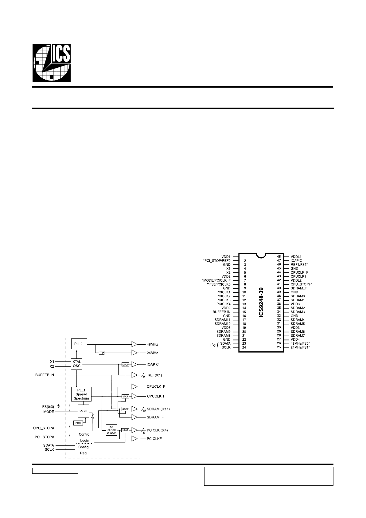
ICS9248-39
Block Diagram
Pentium is a trademark of Intel Corporation
I2C is a trademark of Philips Corporation
Frequency Generator & Integrated Buffers for PENTIUM/Pro
TM
9248-39 Rev F 12/16/99
Pin Configuration
• 3.3V outputs: SDRAM, PCI, REF, 48/24MHz
• 2.5V outputs: CPU, IOAPIC
• 20 ohm CPU clock output impedance
• 20 ohm PCI clock output impedance
• Skew from CPU (earlier) to PCI clock - 1.5 to 4 ns,
center 2.6 ns.
• No external load cap for CL=18pF crystals
• ±175 ps CPU clock skew
• 250ps (cycle to cycle) CPU jitter
• Smooth frequency switch, with selections from 66.8
to 150 MHz CPU.
•I
2
C interface for programming
• 3ms power up clock stable time
• Clock duty cycle 45-55%.
• 48 pin 300 mil SSOP package
• 3.3V operation, 5V tolerant inputs (with series R)
• <5ns propagation delay SDRAM from Buffer Input
48-Pin SSOP
Power Groups
VDD1 = REF (0:1), X1, X2
VDD2 = PCICLK_F, PCICLK(0:4)
VDD3 = SDRAM (0:12), supply for PLL core
VDD4 = 24MHz, 48MHz
VDDL1 = IOAPIC
VDDL2 = CPUCLK 1, CPUCLK_F
* Internal Pull-up Resistor of 240K to VDD
** Internal Pull-down resistor of 240K to GND
The ICS9248-39 generates all clocks required for high speed
RISC or CISC microprocessor systems such as Intel
PentiumPro or Cyrix. Eight different reference frequency
multiplying factors are externally selectable with smooth
frequency transitions.
Features include two CPU, six PCI and thirteen SDRAM
clocks. T wo reference outputs are available equal to the crystal
frequency. Plus the IOAPIC output powered by VDDL1. One
48 MHz for USB, and one 24 MHz clock for Super IO. Spread
Spectrum built in at ±0.5% or ±0.25% modulation to reduce
the EMI. Serial programming I2C interface allows changing
functions, stop clock programing and Frequency selection.
Additionally, the device meets the Pentium power-up
stabilization, which requires that CPU and PCI clocks be
stable within 2ms after power-up. It is not recommended to
use I/O dual function pin for the slots (ISA, PIC, CPU,
DIMM). The add on card might have a pull up or pull down.
High drive PCICLK and SDRAM outputs typically provide
greater than 1 V/ns slew rate into 30pF loads. CPUCLK
outputs typically provide better than 1V/ns slew rate into 20pF
loads while maintaining 50±5% duty cycle. The REF and 24
and 48 MHz clock outputs typically provide better than 0.5V/
ns slew rates into 20pF.
ICS reserves the right to make changes in the device data identified in
this publication without further notice. ICS advises its customers to
obtain the latest version of all device data to verify that any
information being relied upon by the customer is current and accurate.
2
ICS9248-39
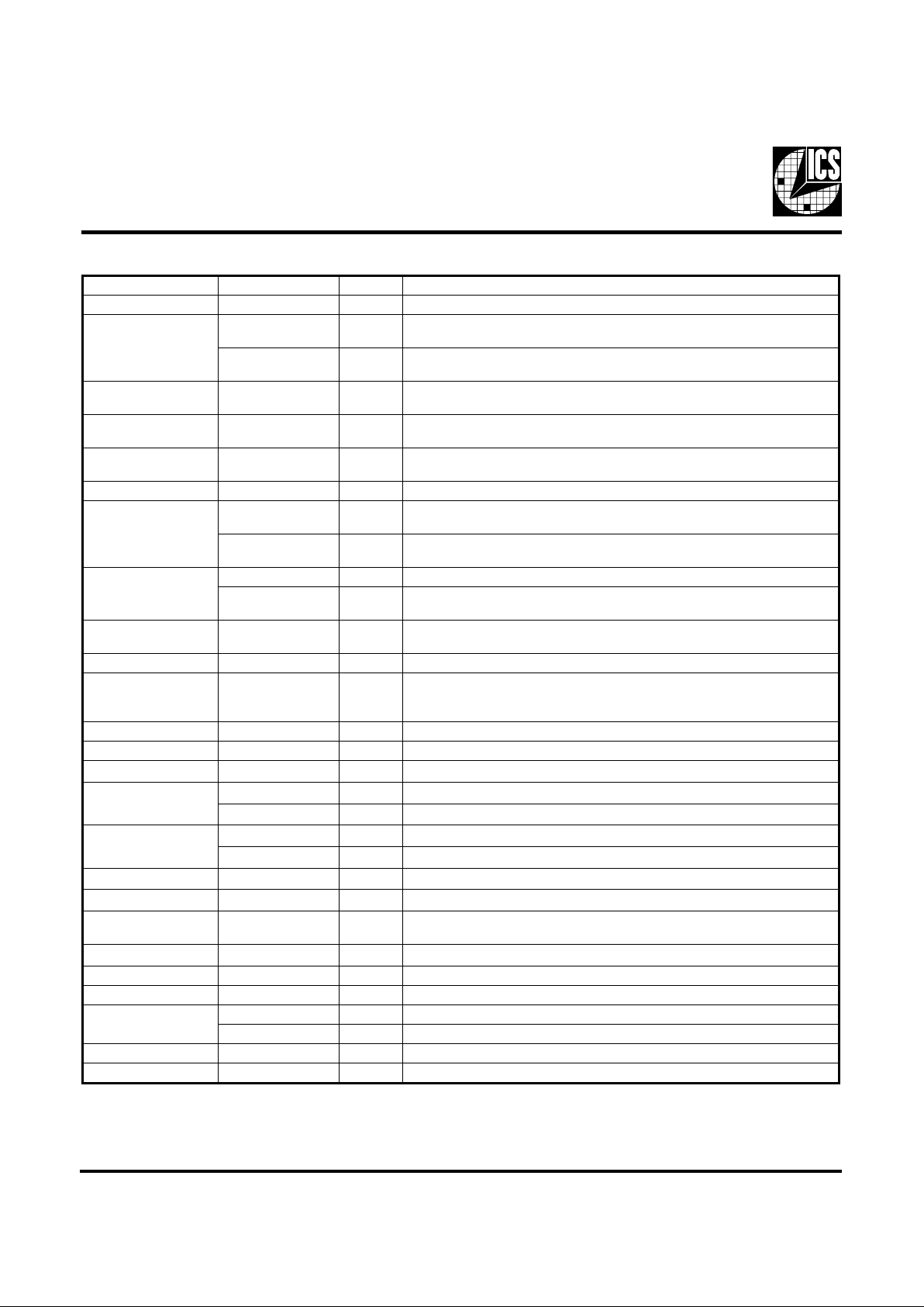
Pin Descriptions
Notes:
1: Internal Pull-up Resistor of 240K to 3.3V on indicated inputs
2: Bidirectional input/output pins, input logic levels are latched at internal power-on-reset. Use 10Kohm resistor
to program logic Hi to VDD or GND for logic low.
REBMUNNIPEMANNIPEPYTNOITPIRCSED
11DDVRWPV3.3lanimon,ylppusrewopLATX,)2:0(feR
2
0FERTUO
REGNORTSehtsituptuoFERsihT.kcolcecnereferzhM813.41
sdaolSUBASIrofreffub
#POTS_ICP
1
NI
nI(woltupninehw,level0cigoltaskcolc)4:0(KLCICPstlaH
)0=EDOM,edomelibom
,22,61,9,3
54,93,33
DNGRWPdnuorG
41XNI
kcabdeefdna)Fp63(pacdaollanretnisah,tupnilatsyrC
2Xmorfrotsiser
52XTUO
daollanretnisaH.zHM813.41yllanimon,tuptuolatsyrC
)Fp63(pac
41,62DDVRWPV3.3lanimon,)4:0(KLCICPdnaF_KLCICProfylppuS
7
F_KLCICPTUO
rewoprof#POTS_ICPybdetceffatonkcolcICPgninnureerF
.tnemeganam
EDOM
2,1
NI
.edoMeliboM=0,edoMpotkseD=1,niptcelesnoitcnuf2niP
.tupnIdehctaL
8
3SFNIDNGotnwod-lluPlanretnI.tupnIdehctaL.niptcelesycneuqerF
0KLCICPTUO
wekssn84-1htiwskcolcUPCotsuonorehcnyS.stuptuokcolcICP
)ylraeUPC(
31,21,11,01)4:1(KLCICPTUO
wekssn84-1htiwskcolcUPCotsuonorehcnyS.stuptuokcolcICP
)ylraeUPC(
51NIREFFUBNI.stuptuoMARDSrofsreffuBtuonaFottupnI
,12,02,81,71
,23,13,92,82
83,73,53,43
)0:11(MARDSTUO
nipNIREFFUBmorfstuptuoreffuBtuonaF,stuptuokcolcMARDS
.)tespihcybdellortnoc(
63,03,913DDVRWP.V3.3lanimon,eroCLLPUPCdna)21:0(MARDSrofylppuS
32ATADSNIIroftupniataD
2
tupnitnarelotV5,tupnilairesC
42KLCSNIIfotupnikcolC
2
tupnitnarelotV5,tupniC
52
zHM42TUOkcolctuptuozHM42
1SF
2,1
NI.tupnIdehctaL.niptcelesycneuqerF
62
zHM84TUOkcolctuptuozHM84
0SF
2,1
NItupnIdehctaL.niptcelesycneuqerF
724DDVRWP.erocLLPdexifdnasreffubtuptuozHM84&42rofrewoP
04F_MARDSTUO#POTS_UPCybdetceffatoN.tuptuokcolcMARDSgninnureerF
14#POTS_UPCNI
MARDS&CIPAOI,1KLCUPCstlahtupnisuonorhcnysasihT
.wolnevirdnehwlevel"0"cigolta)11:0(
242LDDVRWPlanimonV3.3roV5.2rehtie,skcolcUPCrofylppuS
341KLCUPCTUOwoL=#POTS_UPCfiwoL.2LDDVybderewop,stuptuokcolcUPC
44F_KLCUPCTUO#POTS_UPCehtybdetceffatoN.kcolcUPCgninnureerF
64
1FERTUO.kcolcecnereferzHM813.41
2SF
2,1
NItupnIdehctaL.niptcelesycneuqerF
74CIPAOITUOCIPAOI.1LDDVybderewoPzHM813.41.tuptuokcolc
841LDDVRWPlanimonV3.3ro5.2rehtie,CIPAOIrofylppuS
3
ICS9248-39
Functionality
VDD1,2,3 = 3.3V±5%, V
DDL
1,2 = 2.5V±5% or 3.3±5%, TA=0 to 70°C
Crystal (X1, X2) = 14.31818MHz
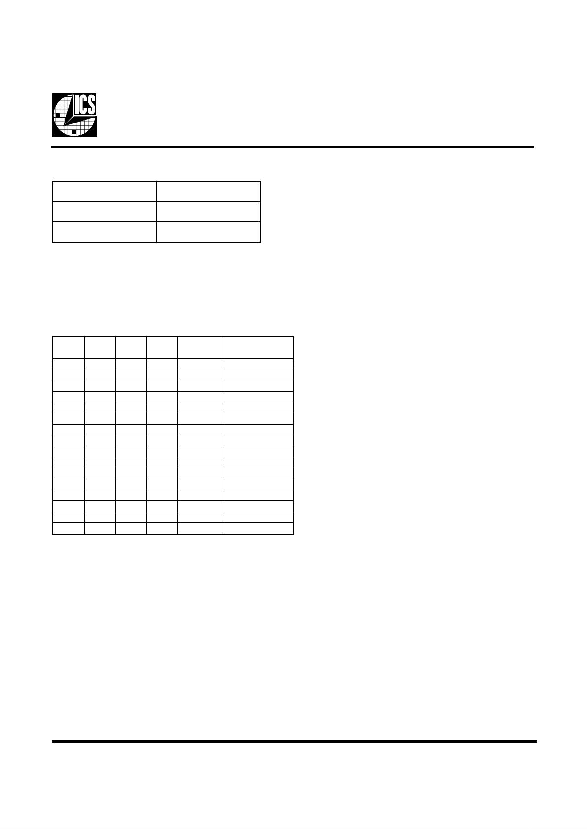
Mode Pin - Power Management Input Control
7niP,EDOM
)tupnIdehctaL(
2niP
0
#POTS_ICP
)tupnI(
1
0FER
)tuptuO(
3SF2SF1SF0SF
UPC
)zHM(
)zHM(KLCICP
1111 331)4/UPC(3.33
1110 421)4/UPC(13
1101 051)4/UPC(5.73
1100 041)4/UPC(53
1011 501)3/UPC(53
1010 011)3/UPC(76.63
1001 511)3/UPC(33.83
1000 021)3/UPC(00.04
0111 3.001)3/UPC(34.33
0110 331)3/UPC(33.44
0101 211)3/UPC(33.73
0100 301)2/UPC(33.43
0011 8.66)2/UPC(04.33
0010 3.38)2/UPC(56.14
0001 57)2/UPC(5.73
0000 421)3/UPC(33.14
4
ICS9248-39
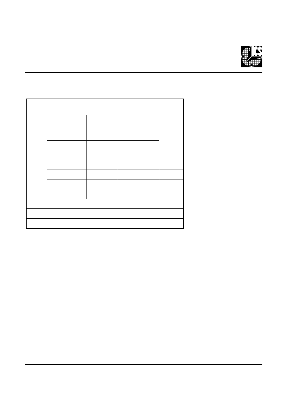
tiBnoitpircseDDWP
7tiB
noitaludoMmurtcepSdaerpS%52.0±-0
noitaludoMmurtcepSdaerpS%5.0±-1
0
4tiB5tiB6tiB2tiBkcolcUPCICP
1etoN
,2tiB
4:6tiB
1110
0110
3.001
331
)3/UPC(34.33
)3/UPC(33.44
1010
0010
211
301
)3/UPC(33.73
)3/UPC(3.43
1100
0100
8.66
3.38
)2/UPC(4.33
)2/UPC(56.14
1000
0000
57
421
)2/UPC(5.73
)3/UPC(33.14
1111
0111
331
421
)4/UPC(52.33
)4/UPC(00.13
1011
0011
051
041
)4/UPC(05.73
)4/UPC(00.53
1101
0101
501
011
)3/UPC(00.53
)3/UPC(76.63
1001
0001
511
021
)3/UPC(33.83
)3/UPC(00.04
3tiB
stupnIdehctaL,tceleserawdrahybdetcelessiycneuqerF-0
)evoba(4:6tiBybdetcelessiycneuqerF-1
0
1tiB
lamroN-0
)daerpSretneC(delbanEmurtcepSdaerpS-1
0
0tiB
gninnuR-0
stuptuollaetatsirT-1
0
Byte0: Functionality and Frequency Select Register (default = 0)
Serial Configuration Command Bitmap
Note: PWD = Power-Up Default
Note 1. Default at Power-up will be for latched logic inputs to define frequency. Bits 4, 5, 6
are default to 000, and if bit 3 is written to a 1 to use Bits 6:4, then these should be
defined to desired frequency at same write cycle.
5
ICS9248-39
Notes:
1. Inactive means outputs are held LOW and are disabled from switching.
2. Latched Frequency Selects (FS#) will be inverted logic load of the input frequency select pin conditions.
Byte 2: PCI Active/Inactive Register (1 = enable, 0 = disable)
tiB#niPDWPnoitpircseD
7tiB-1 )devreseR(
6tiB71 )tcanI/tcA(F_KLCICP
5tiB-1 )devreseR(
4tiB311 )tcanI/tcA(4KLCICP
3tiB211 )tcanI/tcA(3KLCICP
2tiB111 )tcanI/tcA(2KLCICP
1tiB011 )tcanI/tcA(1KLCICP
0tiB81 )tcanI/tcA(0KLCICP
Byte 1: CPU, Active/Inactive Register (1 = enable, 0 = disable)
tiB#niPDWPnoitpircseD
7tiB-X #2SFdehctaL
6tiB-1 )devreseR(
5tiB-1 )devreseR(
4tiB-1 )devreseR(
3tiB041 )tcanI/tcA(21MARDS
2tiB-1 )devreseR(
1tiB341 )tcanI/tcA(1KLCUPC
0tiB441 )tcanI/tcA(F_KLCUPC
Byte 3: SDRAM Active/Inactive Register (1 = enable, 0 = disable)
tiB#niPDWPnoitpircseD
7tiB-1 )devreseR(
6tiB-X #0SFdehctaL
5tiB621 )tcanI/tcA(zHM84
4tiB521 )tcanI/tcA(zHM42
3tiB-1 )devreseR(
2tiB71,81,02,121 )evitcanI/evitcA()11:8(MARDS
1tiB82,92,13,231 )evitcanI/evitcA()7:4(MARDS
0tiB43,53,73,831 )evitcanI/evitcA()3:0(MARDS

6
ICS9248-39
Byte 4: Reserved Active/Inactive Register (1 = enable, 0 = disable)
Byte 5: Peripheral Active/Inactive Register (1 = enable, 0 = disable)
Notes:
1. Inactive means outputs are held LOW and are disabled from switching.
2. Latched Frequency Selects (FS#) will be inverted logic load of the input frequency select pin conditions.
tiB#niPDWPnoitpircseD
7tiB-1 )devreseR(
6tiB-1 )devreseR(
5tiB-1 )devreseR(
4tiB-1 )devreseR(
3tiB-X #1SFdehctaL
2tiB-1 )devreseR(
1tiB-X #3SFdehctaL
0tiB-1 )devreseR(
tiB#niPDWPnoitpircseD
7tiB-1 )devreseR(
6tiB-1 )devreseR(
5tiB-1 )devreseR(
4tiB741 )tcanI/tcA(0CIPAOI
3tiB-1 )devreseR(
2tiB-1 )devreseR(
1tiB641 )tcanI/tcA(1FER
0tiB21 )tcanI/tcA(0FER

7
ICS9248-39
Absolute Maximum Ratings
Supply Voltage. . . . . . . . . . . . . . . . . . . . . . . . . . . 5.5 V
Logic Inputs. . . . . . . . . . . . . . . . . . . . . . . . . . . . . GND –0.5 V to VDD +0.5 V
Ambient Operating Temperature . . . . . . . . . . . . 0°C to +70°C
Case Temperature . . . . . . . . . . . . . . . . . . . . . . . . 115°C
Storage Temperature . . . . . . . . . . . . . . . . . . . . . . –65°C to +150°C
Stresses above those listed under Absolute Maximum Ratings may cause permanent damage to the device. These ratings are stress
specifications only and functional operation of the device at these or any other conditions above those listed in the operational
sections of the specifications is not implied. Exposure to absolute maximum rating conditions for extended periods may affect
product reliability.
Electrical Charact eri sti cs - I nput/ Supply/ Com m on O utput Parameters
TA = 0 - 70º C; Supply Voltage V
DD, VDDL
= 3.3 V +/-5% (unless otherwi se stat e d)
PARAMETER SYMBOL CONDITIONS MIN TYP MAX UNITS
Input High Voltage V
IH
2V
DD
+0.3 V
Input L ow Voltage V
IL
VSS-0.3 0.8 V
Inpu t High C urrent I
IH
VIN = V
DD
0.1 5
µ
A
Input Low Current I
IL1
VIN = 0 V; Inputs w i th no pul l-up resist ors - 5 2.0
µ
A
Input Low Current I
IL2
VIN = 0 V; Inputs w i th pull- up resis to rs -200 -10 0
µ
A
Operating I
DD3.3OP66CL
= 0 pF; Sele c t @ 66MHz 146
Suppl y C urrent I
DD3.3OP100CL
= 0 pF; Sele c t @ 100MHz 174
Input fr e que nc y F
i
VDD = 3.3 V ; 12 14. 318 16 MHz
Input Capacita nce
1
C
IN
Logic Inputs 5 pF
C
INX
X 1 & X2 pins 27 36 45 pF
Clk Stabiliza tion
1
T
STAB
From VDD = 3.3 V to 1% ta rget F req.
3ms
1
G ua rant eed by design, not 100% tested in production.
mA180
Electrical Characterist ics - I nput/ S upply/Common Ou tput Parameters
TA = 0 - 70º C; Supply Voltage VDD = 3.3 V +/-5%, V
DDL
= 2. 5 V +/-5% (unless otherwise stated)
PARAMETER SYMBOL CONDITIONS MIN TYP MAX UNITS
Operating I
DD2.5OP66
CL = 0 pF; Select @ 66.8 MHz 4 72
Supply Current I
DD2.5OP100CL
= 0 pF; Select @ 100 MHz 6 100
Skew1
t
CPU-P CI
VT = 1.5 V; VTL = 1.25 V
1.5 2.5 4 ns
1
Guara nt eed by de sign, n ot 100% t ested in pr od uc t ion.
mA

8
ICS9248-39
Ele ctrical Characteristi cs - CPUCLK
TA = 0 - 70º C; VDD = 3.3 V +/-5%, V
DDL
= 2.5 V +/-5%; CL = 20 pF (unless ot he rwis e state d )
PARAMETER SYMBOL CONDITIONS MIN TYP MAX UNITS
Output High Voltage V
OH2B
IOH = -12.0 mA 2 2.23 V
Output Low Voltage V
OL2B
IOL = 12 mA 0.32 0.4 V
O utput High C urr e nt I
OH2B
VOH = 1 .7 V -32 -19 mA
Ou tput Low Curr e nt I
OL2B
VOL = 0.7 V 19 25 mA
Rise Time t
r2B
1
VOL = 0.4 V , VOH = 2.0 V 1.48 1.6 ns
Fall Time t
f2B
1
VOH = 2.0 V, VOL = 0.4 V 1.25 1.6 ns
Duty Cycle d
t2B
1
VT = 1.25 V 454555%
Skew t
sk2B
1
VT = 1.25 V 125 175 ps
Jitter, C ycle-to- c ycle t
jcyc-cyc2B
1
VT = 1.25 V 225 250 ps
Jitter, One Sigma t
j1s2B
1
VT = 1.25 V 36 150 ps
Jitter, Absolute
t
jabs2B
1
VT = 1.25 V
-250 130 +250 ps
1
G ua rant eed by design, not 100% tested in production.
Electrical Characteristics - PCICLK
TA = 0 - 70º C; VDD = 3.3 V +/-5%, V
DDL
= 2.5 V +/-5%; CL = 30 pF (unless ot he rwis e state d )
PARAMETER SYMBOL CONDITIONS MIN TYP MAX UNITS
O utput High Vol t ag e V
OH1
IOH = -11 mA 2.4 3.05 V
Output Low Voltage V
OL1
IOL = 9.4 mA 0.17 0.4 V
Ou tput High Current I
OH1
VOH = 2.0 V -52 -22 m A
Output Low Current I
OL1
VOL = 0.8 V 25 40 mA
Rise Time
1
t
r1
VOL = 0.4 V, VOH = 2.4 V 2 2 ns
Fall Time
1
t
f1
VOH = 2.4 V , VOL = 0.4 V 1.65 2 ns
Duty Cycle
1
d
t1
VT = 1.5 V 45 49 55 %
Skew
1
t
sk1
VT = 1.5 V 240 500 ps
Jitter, C ycle-to- c ycle t
jcyc-cyc2B
1
VT = 1.5 V 210 250 ps
Jitter , One Si gma
1
t
j1s1
VT = 1.5 V 18 150 ps
Jitter , Absolute
1
t
jabs1
VT = 1.5 V
-500 90 500 ps
1
Guara nt eed by design, not 100 % tested in product ion.

9
ICS9248-39
Ele ctrica l Characteristics - SD RAM
TA = 0 - 70º C; VDD = 3.3 V +/-5%, V
DDL
= 2.5 V +/-5%; CL = 30 pF (unless ot he rwis e state d )
PARAMETER SYMBOL CONDITIONS MIN TYP MAX UNITS
Output High Voltage V
OH3
IOH = -28 mA 2.4 2.9 V
Output Low Voltage V
OL3
IOL = 23 mA 0.4 0.4 V
O utput High Current I
OH3
VOH = 2 .0 V -77 -54 mA
Ou tput Low Curr e nt I
OL3
VOL = 0.8 V 41 41 mA
Rise Time T
r3
1
VOL = 0.4 V , VOH = 2.4 V 1.5 2 ns
Fall Time T
f3
1
VOH = 2.4 V, VOL = 0.4 V 1.8 2 ns
Duty Cycle D
t3
1
VT = 1.5 V 45 49.5 55 %
Skew
1
T
sk1
VT = 1.5 V 190 500 ps
Propagation Delay Tprop VT = 1 .5 V 3 5 ns
1
G ua renteed by de sign, not 100% te sted in produ c t i on.
Electrical Characteristics - IOAPIC
TA = 0 - 70º C; VDD = 3.3 V +/-5%, V
DDL
= 2.5 V +/-5%; CL = 20 pF (unless ot he rwis e state d )
PARAMETER SYMBOL CONDITIONS MIN TYP MAX UNITS
O utput High Vol t ag e V
OH4BIOH
= -12 mA 2 2.12 V
Output Low Voltage V
OL4BIOL
= 12 mA 0.32 0.4 V
Ou tput High Current I
OH4B
VOH = 1.7 V -23 -19 m A
Output Low Current I
OL4B
VOL = 0.7 V 19 25 mA
Rise Time
1
T
r4B
VOL = 0.4 V, VOH = 2.0 V 1.45 2 ns
Fall Time
1
T
f4B
VOH = 2.0 V , VOL = 0.4 V 1.3 2 ns
Duty Cycle
1
D
t4B
VT = 1.25 V 45 51 55 %
Jitter , One Si gma
1
T
j1s4B
VT = 1.25 V 0.2 0.5 ns
Jitter , Absolute
1
T
jabs4B
VT = 1.25 V
-1 0.5 1 ns
1
Guara nt eed by design, not 100 % tested in product ion.

10
ICS9248-39
Ele ctrica l Charact erist ics - 24MHz, 48MHz, REF(0:1)
TA = 0 - 70º C; VDD = 3.3 V +/-5%, V
DDL
= 2.5 V +/-5%; CL = 20 pF (unless ot he rwis e state d )
PARAMETER SYMBOL CONDITIONS MIN TYP MAX UNITS
O utput High Vol t ag e V
OH5
IOH = -16 mA 2.4 2.73 V
Output Low Voltage V
OL5
IOL = 9 mA 0.23 0.4 V
Ou tput High Current I
OH5
VOH = 2.0 V -32 -22 m A
Output Low Current I
OL5
VOL = 0.8 V 16 28 mA
Rise Time
1
t
r5
VOL = 0.4 V, VOH = 2.4 V 1.8 4 ns
Fall Time
1
t
f5
VOH = 2.4 V , VOL = 0.4 V 1.8 4 ns
Duty Cycle
1
d
t5
VT = 1.5 V 45 51 55 %
Jitter , One Si gma
1
t
j1s5
VT = 1.5 V 0.2 0.5 ns
Jitter , Absolute
1
t
jabs5
VT = 1.5 V
-1 0.5 1 ns
1
Guara nt eed by design, not 100 % tested in product ion.

11
ICS9248-39
1 . The ICS clock generator is a slave/receiver, I2C component. It can read back the data stored in the latches for verification.
Read-Back will support Intel PIIX4 "Block-Read" protocol.
2. The data transfer rate supported by this clock generator is 100K bits/sec or less (standard mode)
3 . The input is operating at 3.3V logic levels.
4. The data byte format is 8 bit bytes.
5. To simplify the clock generator I2C interface, the protocol is set to use only "Block-Writes" from the controller. The
bytes must be accessed in sequential order from lowest to highest byte with the ability to stop after any complete byte
has been transferred. The Command code and Byte count shown above must be sent, but the data is ignored for those
two bytes. The data is loaded until a Stop sequence is issued.
6. At power-on, all registers are set to a default condition, as shown.
General I2C serial interface information
The information in this section assumes familiarity with I2C programming.
For more information, contact ICS for an I2C programming application note.
How to Write:
• Controller (host) sends a start bit.
• Controller (host) sends the write address D2
(H)
• ICS clock will acknowledge
• Controller (host) sends a dummy command code
• ICS clock will acknowledge
• Controller (host) sends a dummy byte count
• ICS clock will acknowledge
• Controller (host) starts sending first byte (Byte 0)
through byte 5
• ICS clock will acknowledge each byte one at a time.
• Controller (host) sends a Stop bit
How to Read:
• Controller (host) will send start bit.
• Controller (host) sends the read address D3
(H)
• ICS clock will acknowledge
• ICS clock will send the byte count
• Controller (host) acknowledges
• ICS clock sends first byte (Byte 0) through byte 5
• Controller (host) will need to acknowledge each byte
• Controller (host) will send a stop bit
Notes:
Controller (Host) ICS (Slave/Receiver)
Start Bit
Address
D3
(H)
A
CK
Byte Count
ACK
Byte 0
ACK
Byte 1
ACK
Byte 2
ACK
Byte 3
ACK
Byte 4
ACK
Byte 5
ACK
Stop Bit
How to Read:
Controller (Host) ICS (Slave/Receiver)
Start Bit
Address
D2
(H)
A
CK
Dummy Command Code
A
CK
Dummy Byte Count
A
CK
Byte 0
A
CK
Byte 1
ACK
Byte 2
A
CK
Byte 3
A
CK
Byte 4
A
CK
Byte 5
A
CK
Stop Bit
How to Write:

12
ICS9248-39
CPU_STOP# Timing Diagram
CPU_STOP# is an asychronous input to the clock synthesizer. It is used to turn off the CPU clocks for low power operation.
CPU_STOP# is synchronized by the ICS9248-39. The minimum that the CPU clock is enabled (CPU_STOP# high pulse) is
100 CPU clocks. All other clocks will continue to run while the CPU clocks are disabled. The CPU clocks will always be stopped
in a low state and start in such a manner that guarantees the high pulse width is a full pulse. CPU clock on latency is less than
4 CPU clocks and CPU clock off latency is less than 4 CPU clocks.
Notes:
1. All timing is referenced to the internal CPU clock.
2. CPU_STOP# is an asynchronous input and metastable conditions may exist. This signal is synchronized
to the CPU clocks inside the ICS9248-39.
3. IOAPIC output is Stopped Glitch Free by CPUSTOP# going low.
4. SDRAM-F output is controlled by Buffer in signal, not affected by the ICS9248-39
CPU_STOP# signal. SDRAM (0:11) are controlled as shown.
5. All other clocks continue to run undisturbed.

13
ICS9248-39
PCI_STOP# Timing Diagram
PCI_STOP# is an asynchronous input to the ICS9248-39. It is used to turn off the PCICLK (0:4) clocks for low power operation.
PCI_STOP# is synchronized by the ICS9248-39 internally. The minimum that the PCICLK (0:4) clocks are enabled
(PCI_STOP# high pulse) is at least 10 PCICLK (0:4) clocks. PCICLK (0:4) clocks are stopped in a low state and started with
a full high pulse width guaranteed. PCICLK (0:4) clock on latency cycles are only one rising PCICLK clock off latency is one
PCICLK clock.
Notes:
1. All timing is referenced to the Internal CPUCLK (defined as inside the ICS9248 device.)
2. PCI_STOP# is an asynchronous input, and metastable conditions may exist. This signal is required to be synchronized
inside the ICS9248.
3. All other clocks continue to run undisturbed.
4. CPU_STOP# is shown in a high (true) state.

14
ICS9248-39
Fig. 1
Shared Pin Operation Input/Output Pins
The I/O pins designated by (input/output) on the ICS924839 serve as dual signal functions to the device. During initial
power-up, they act as input pins. The logic level (voltage)
that is present on these pins at this time is read and stored
into a 5-bit internal data latch. At the end of Power -On reset,
(see AC characteristics for timing values), the device changes
the mode of operations for these pins to an output function.
In this mode the pins produce the specified buffered clocks
to external loads.
T o program (load) the internal configuration register for these
pins, a resistor is connected to either the VDD (logic 1) power
supply or the GND (logic 0) voltage potential. A 10 Kilohm
(10K) resistor is used to provide both the solid CMOS
programming voltage needed during the power-up
programming period and to provide an insignificant load on
the output clock during the subsequent operating period.
Via to
VDD
Clock trace to load
Series Term. Res.
Programming
Header
Via to Gnd
Device
Pad
2K
8.2K
Figure 1 shows a means of implementing this function when
a switch or 2 pin header is used. W ith no jumper is installed
the pin will be pulled high. W ith the jumper in place the pin
will be pulled low. If programmability is not necessary, than
only a single resistor is necessary . The programming resistors
should be located close to the series termination resistor to
minimize the current loop area. It is more important to locate
the series termination resistor close to the driver than the
programming resistor.

15
ICS9248-39
General Layout Precautions:
1) Use a ground plane on the top layer
of the PCB in all areas not used by
traces.
2) Make all power traces and vias as
wide as possible to lower inductance.
Notes:
1 All clock outputs should have series
terminating resistor. Not shown in all
places to improve readibility of
diagram
2 Optional EMI capacitor should be
used on all CPU, SDRAM, and PCI
outputs.
3 Optional crystal load capacitors are
recommended.
Capacitor Values:
C1, C2 : Crystal load values determined by user
C3 : 100pF ceramic
All unmarked capacitors are 0.01F ceramic

16
ICS9248-39
ICS reserves the right to make changes in the device data identified in
this publication without further notice. ICS advises its customers to
obtain the latest version of all device data to verify that any
information being relied upon by the customer is current and accurate.
Ordering Information
ICS9248yF-39
Pattern Number (2 or 3 digit number for parts with ROM code patterns)
Package Type
F=SSOP
Revision Designator (will not correlate with datasheet revision)
Device Type (consists of 3 or 4 digit numbers)
Prefix
ICS, AV = Standard Device
Example:
ICS XXXX y F - PPP
.093
DIA. PIN (Optional)
D/2
E/2
BOTTOM VIEW
A
1
-e-
B
A
SIDE VIEW
-C-
-D-
SEATING
PLANE
A
2
SEE
DETAIL “A”
-E-
C
END VIEW
PARTING LINE
L
DETAIL “A”
H
Pin 1
TOP VIEW
Index
Area
LOBMYSSNOISNEMIDNOMMOCSNOITAIRAVDN
.NIM.MON.XAM.NIM.MON.XAM
A590.201.011.CA026.526.036.84
1A800.210.610.
2A780.090.490.
B800.-5310.
C500.- 5800.
DsnoitairaVeeS
E192.592.992.
eCSB520.0
H593.-024.
h010.310.610.
L020.-040.
NsnoitairaVeeS
µ
°0- °8
48 Pin 300 mil SSOP Package
“For current dimensional specifications, see JEDEC 95.”
 Loading...