

Integrated
Circuit
Systems, Inc.
ICS9248-157
Third party brands and names are the property of their respective owners.
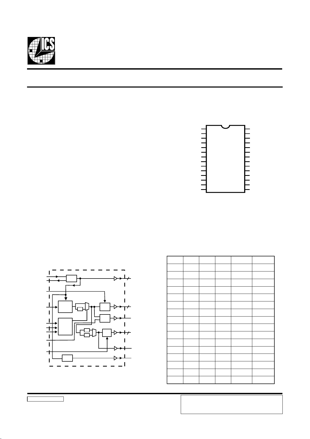
Block Diagram
9248-157 Rev A - 1/16/01
Functionality
Pin Configuration
28 Pin 209mil SSOP
Recommended Application:
ALI1621/1632M style chipsets
Output Features:
• 2 - CPUs @2.5V, up to 140MHz.
• 7 - PCI @3.3V, (including one free running)
• 1 - 48MHz, @3.3V fixed.
• 2 - REF @3.3V, 14.318MHz.
Features:
• Up to 140 MHz frequency support
• Support power management: CPU, PCI stop and
Power down.
• Spread spectrum for EMI control (0.5% down spread).
• Uses external 14.318MHz crystal
• FS pins for frequency select
Key Specifications:
• CPU – CPU: <175ps
• PCI – PCI: <250ps
• CPU(early)-PCI: 1.5ns - 4ns
• PCI_E (early) - PCI: 2.1ns
Frequency Timing Generator for Pentium II Systems
FS (3:0)
CPU_STOP#
X1
X2
OSC
PLL
Spread
Spectrum
Glitch
Free
Control
Logic
REF (1:0)
2
5
PCICLK (4:0),
PCICLK_E
48MHz
PCI_STOP#
SEL_CPUF#
PD#
Div4#
/4
BUS
STOP
PCICLK_F
PLL2
2
CPUCLK 1
CPUCLK0/F
CPU
STOP
CPU
STOP
/2
/3
SPREAD#
3SF2SF1SF0SFUPCICP
0000 33.3366.61
0001 33.3666.13
0010 99.9600.53
0011 66.6633.33
0100 00.7933.23
0101 22.6970.23
0110 05.1905.03
0111 33.3877.72
1000 00.0566.61
100 1 52.5957.13
10 10 00.50100.53
10 11 00.00133.33
1100 66.6666.61
110 1 53.62166.13
1110 56.93100.53
1111 33.33133.33
*These inputs have a 120K pull up to VDD
**These inputs have a 120K pull down to GND
*FS1/REF0
X1
X2
**FS2/PCICLK_F
*SEL_CPUF#/PCICLK0
PCICLK1
GND
VDDPCI
PCICLK2
PCICLK3
PCICLK4
PCICLK_E
VDD48
*FS3/48MHz
VDDR
REF1/FS0*
SPREAD#
VDDL
CPUCLK1
CPUCLK0/F
GNDL
GND
PCI_STOP#
VDDA
CPU_STOP#
PD#
DIV/4#
GND
ICS9248-157
1
2
3
4
5
6
7
8
9
10
11
12
13
14
28
27
26
25
24
23
22
21
20
19
18
17
16
15
ICS reserves the right to make changes in the device data
identified in this publication without further notice. ICS advises
its customers to obtain the latest version of all device data to
verify that any information being relied upon by the customer is
2
ICS9248-157
Advance Information
Third party brands and names are the property of their respective owners.
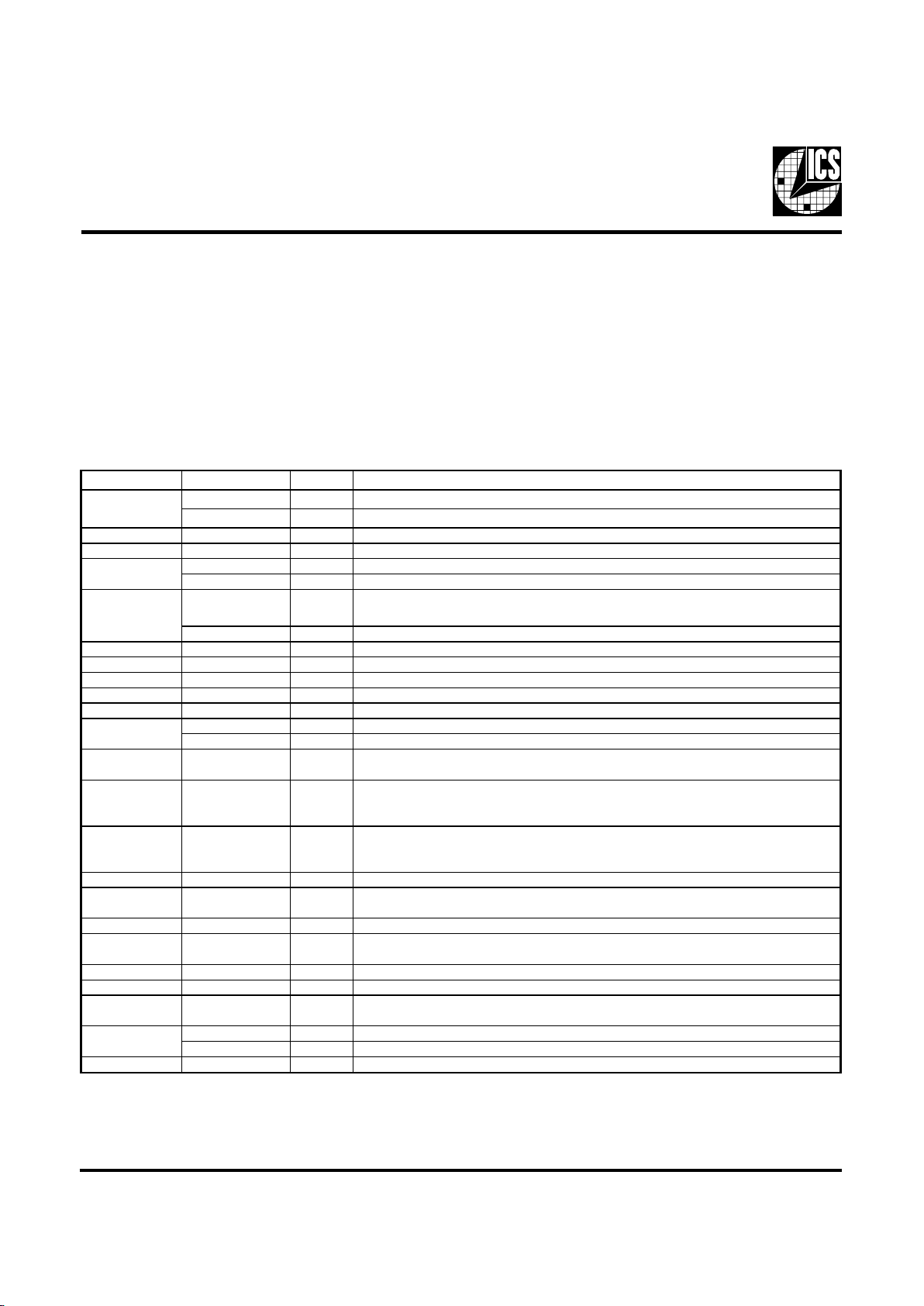
Pin Descriptions
General Description
The ICS9248-157 is the Main clock solution for Notebook designs using the Intel ALI1621/1632M style chipset. Along with
an SDRAM buffer such as the ICS9179-03, it provides all necessary clock signals for such a system.
Spread spectrum may be enabled by driving pin 26, SPREAD# active (Low) at power-on. Spread spectrum typically reduces
system EMI by 8dB to 10dB. This simplifies EMI qualification without resorting to board design iterations or costly shielding.
The ICS9248-157 employs a proprietary closed loop design, which tightly controls the percentage of spreading over process
and temperature variations.
Pin number Pin name Type Description
FS1 Input Frequency selec t pin
REF0 Output 3.3V, 14.318 MHz reference clock output.
2 X1 Input 14.318 MHz crystal input
3 X2 Output 14.318 MHz crystal output
FS2 Input Frequency selec t pin
PCICLK _F Output 3.3 V free running PCI c lock output, will not be stopped by the PCI_STO P#
SEL_CPUF# Input
Active low input to select CPUCLK 0/F (pin 23) either normal CPUCLK or Free
running (not stoppable through CPU_STOP#) clock.
PCICLK 0 Output 3.3V P CI clock output
11, 10, 9, 6 PCICLK (4:1) Output 3.3 V PCI clock outputs, generating timing requirements
7, 15, 21 GND Power Ground for clock outputs
8 VDDPCI Power 3.3 V power for the PCI cloc k outputs
12 PCICLK_E Output Early PCICLK output, offset from other PCICLKs, stopped by PCI-STOP#
13 VDD48 Power 3.3 V power for 48 MHz clocks
FS3 Input Frequency selec t pin
48MHz Output Fixed 48MHz clock.
16 DIV 4# Input
Active low input, enables the CP UCLK and the P CICLK to run at 1/4 of the regular
frequecies
17 PD# Input
Asynchronous active low input pin used to power down the device into a low power
state. The internal clocks are disabled and the V
CO
and the crystal are stopped. The
latency of the power down will not be greater than 3ms.
18 CP U_STOP # Input
Asynchronous active low input pin used to stop the CPUCLK in active low state, all
other clocks will continue to run. The CPUCLK will have a "Turnon " latency of at
least 3 CPU clocks.
19 VDDA Power 3.3 V power for the core
20 PCI-S TOP# Input
Synchronous ac tive low input used to stop the PCICLK in active low state. I t will not
effect PCICLK_F or any other outputs.
22 GNDL Power Ground for the CPU and Host cloc k outputs
23 CPUCLK0/F Output
2.5V CPU clock output; can be selected to be free running by driving
SEL_CPUF# low
24 CPUCLK1 0utput 2.5 V CP U and Host clock outputs
25 VDDL Power 2.5 V power for the CPU and Host clock outputs
26 S PREAD# Input
power-on spread spectrum enable option. Active low = spread spectrum c locking
enable. Ac tive high = spread spectrum clocking disable.
FS0 Input Frequency selec t pin
REF1 Output 3.3V, 14.318 MHz reference clock output.
28 V DDR Power 3.3 V power for the REFCLK and c rys tal clock outputs
14
1
27
4
5
3
ICS9248-157
Third party brands and names are the property of their respective owners.
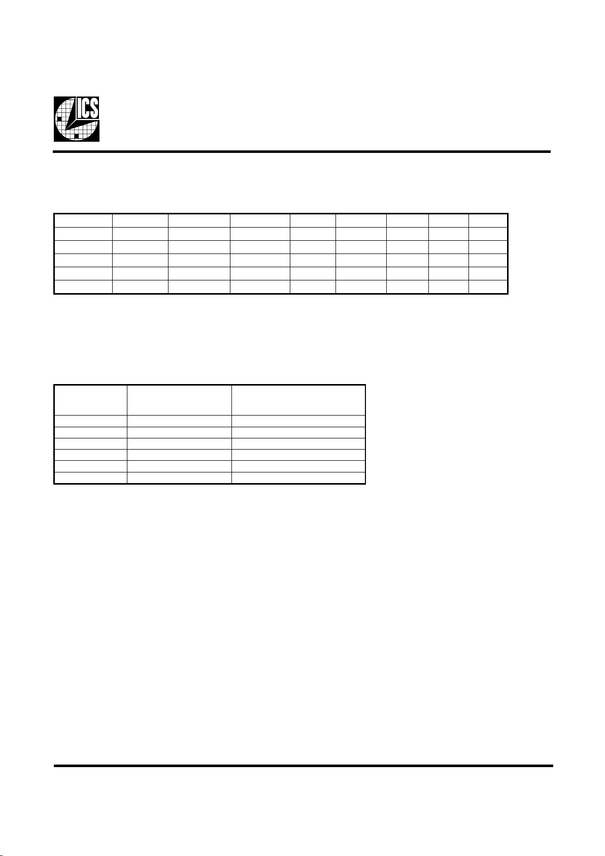
Power Management
Power Management Requirements
Clock Enable Configuration
Full clock cycle timing is guaranteed at all times after the system has initially powered up except where noted. During power up
and power down operations using the PD# pin will not cause clocks of a short or longer pulse than that of the running clock.
The first clock pulse coming out of a stopped clock condition may be slightly distorted due to clock network charging circuitry.
Board routing and signal loading may have a large impact on the initial clock distortion also.
Notes.
1. Clock on latency is defined from when the clock enable goes active to when the first valid clock comes out of the device.
2. Clock off latency is defined from when the clock enable goes inactive to when the last clock is driven low out of the device.
3. Power up latency is when PD# goes inactive (high) to when the first valid clocks are output by the device.
4. Power down has controlled clock counts applicable to CPUCLK, PCICLK only.
The REF will be stopped independant of these.
LANGISETATSLANGIS
ycnetaL
gninnureerffosegdegnisirfo.oN
KLCICP
#POTS_UPC)delbasiD(0
2
1
)delbanE(1
1
1
#POTS_ICP)delbasiD(0
2
1
)delbanE(1
1
1
#DP)noitarepOlamroN(1
3
sm3
)nwoDrewoP(0
4
xam2
#POTS_UPC#POTS_ICP#NWD_RWPKLCUPCKLCICPF_KLCICPFERlatsyrCsOCV
XX 0 woLwoLwoLdeppotSffOffO
00 1 woLwoLgninnuRgninnuRgninnuRgninnuR
01 1 woLgninnuRgninnuRgninnuRgninnuRgninnuR
10 1 gninnuRwoLgninnuRgninnuRgninnuRgninnuR
11 1 gninnuRgninnuRgninnuRgninnuRgninnuRgninnuR
Power Groups:
VDDA = PLL Core
VDD48 = 48MHz Core
VDDPCI = PCICLK
VDDL = CPUCLK
VDDR = Xtal & REF
4
ICS9248-157
Advance Information
Third party brands and names are the property of their respective owners.
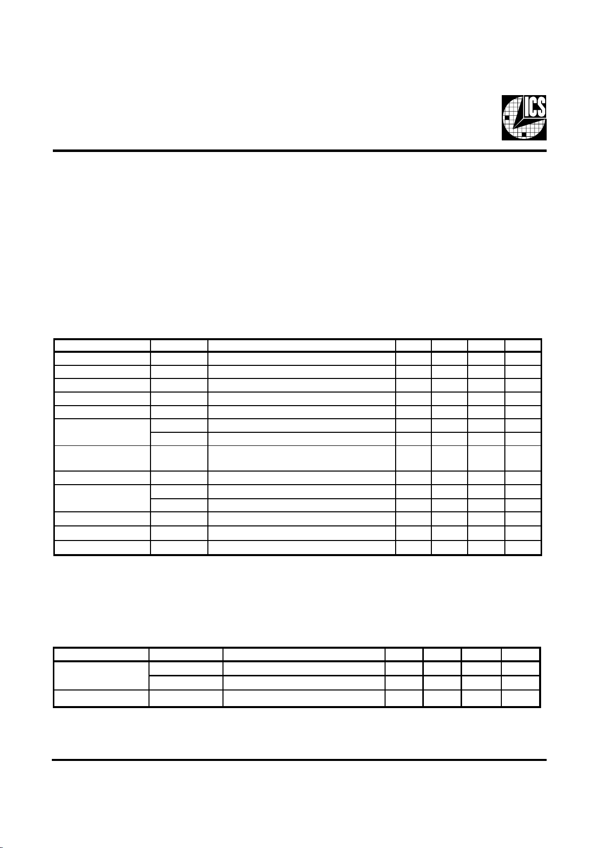
Absolute Maximum Ratings
Supply Voltage . . . . . . . . . . . . . . . . . . . . . . . . . . . . 5.5 V
Logic Inputs . . . . . . . . . . . . . . . . . . . . . . . . . . . . . . GND –0.5 V to V
DD
+0.5 V
Ambient Operating Temperature . . . . . . . . . . . . . 0°C to +70°C
Storage Temperature . . . . . . . . . . . . . . . . . . . . . . . –65°C to +150°C
Stresses above those listed under Absolute Maximum Ratings may cause permanent damage to the device. These ratings are
stress specifications only and functional operation of the device at these or any other conditions above those listed in the
operational sections of the specifications is not implied. Exposure to absolute maximum rating conditions for extended periods
may affect product reliability.
Electrical Characteristics - Input/Sup ply/Common Output Parameters
TA = 0 - 70C; Supply Voltage VDD = 3.3 V +/-5% VDDL = 2.5 V +/-5% (unless otherwise state
d)
PARAMETER
S
YMBOL
CO
NDITION
S
MIN TYP MAX UNIT
S
Input High Voltage V
IH
2V
DD
+0.3 V
Input Low Voltage V
IL
VSS-0.3 0.8 V
Input High Current I
IH
VIN = V
DD
0.1 5
µ
A
Input Low Current I
IL1
VIN = 0 V; Inputs with no pull-up resistors -5 2.0
µ
A
Input Low Current I
IL2
VIN = 0 V; Inputs with pull-up resistors -200 -100
µ
A
Operating I
DD3.3OP66CL
= 0 pF; Select @ 66MHz 60 180 mA
Supply Current I
DD3.3OP100CL
= 0 pF; Select @ 100MHz 66 180 mA
Power Down I
DD3.3PD
CL = 0 pF; With input address to Vdd or GND 70 600
µ
A
Supply Current
Input frequency F
i
VDD = 3.3 V; 11 14.318 16 MHz
Input Capacitance
1
C
IN
Logic Inputs 5 pF
C
INX
X1 & X2 pins 27 36 45 pF
Transition Time
1
T
trans
To 1st crossing of target Freq. 3 ms
Clk Stabilization
1
T
STAB
From VDD = 3.3 V to 1% target Freq. 3 ms
Sk
ew
1
T
CPU-PCI1
VT = 1.5 V;
1.5 2.3 4 ns
1
Guaranteed by design, not 100% tested in production.
Electrical Characteristics - Input/Supply/Common Output Parameters
TA = 0 - 70C; Supply Voltage VDD = 3.3 V +/-5%, V
DDL
= 2.5 V +/-5% (unless otherwise stated )
PARAMETER SYMBOL CONDITIONS MIN TYP MAX UNITS
Operating I
DD2.5OP66
CL = 0 pF; Select @ 66.8 MHz 16 72 mA
Supply Current I
DD2.5OP100
CL = 0 pF; Select @ 100 MHz 23 100 mA
Skew
1
t
CPU-PCI2
VT = 1.5 V; VTL = 1.25 V
1.5 3 4 ns
1
Guaranteed by design, not 100% tested in production.

5
ICS9248-157
Third party brands and names are the property of their respective owners.
Electrical Characteristics - CPUCLK
TA = 0 - 70C; VDD = 3.3 V +/-5%, V
DDL
= 2.5 V +/-5%;
C
L
= 10 - 20 pF (unless otherwise state
d)
PARAMETER
S
YMBOL
CO
NDITION
S
MIN TYP MAXUNIT
S
Output High Voltage V
OH2B
IOH = -12.0 mA 2 2.3 V
Output Low Voltage V
OL2B
IOL = 12 mA 0.2 0.4 V
Output High Current I
OH2B
VOH = 1.7 V -41 -19 mA
Output Low Current I
OL2B
VOL = 0.7 V 19 37 mA
Rise Time t
r2B
1
VOL = 0.4 V, VOH = 2.0 V 0.99 1.6 ns
Fall Time t
f2B
1
VOH = 2.0 V, VOL = 0.4 V 1.05 1.6 ns
Duty Cycle d
t2B
1
VT = 1.25 V 45 50.3 55 %
Skew t
sk2B
1
VT = 1.25 V 34 175 ps
Jitter, Cycle-to-cycle t
jcyc-cyc2B
1
VT = 1.25 V 203 250 ps
Jitter, One Sigma t
j1s2B
1
VT = 1.25 V 150 ps
Jitter, Absolute
t
jabs2B
1
VT = 1.25 V
-250 +250 ps
1
Guaranteed by design, not 100% tested in production.
Electrical Characteristics - PCICLK
TA = 0 - 70C; VDD = 3.3 V +/-5% VDDL = 2.5 V +/-5%; CL = 30 pF
PARAMETER SYMBOL CONDITIONS MIN T YP MAX UNITS
Output High Voltage V
OH1
IOH = -11 mA 2.4 3.1 V
Output Low Voltage V
OL1
IOL = 9.4 mA 0.1 0.4 V
Output High Current I
OH1
VOH = 2.0 V -62 -22 mA
Output Low Current I
OL1
VOL = 0.8 V 16 57 mA
Rise Time
1
t
r1
VOL = 0.4 V, VOH = 2.4 V 1.5 2 ns
Fall Time
1
t
f1
VOH = 2.4 V, VOL = 0.4 V 1.1 2 ns
Duty Cycle
1
d
t1
VT = 1.5 V 455055%
Skew
1
t
sk1
VT = 1.5 V 290 500 ps
Jitter, Cycle-to-cycle t
jcyc-cyc1
VT = 1.25 V 200 500 ps
Jitter, One Sigma
1
t
j
1s1
VT = 1.5 V 150 ps
Jitter, Absolute
1
t
jabs1
VT = 1.5 V
-250 250 ps
1
Guaranteed by design, not 100% tested in production.

6
ICS9248-157
Advance Information
Third party brands and names are the property of their respective owners.
Electrical Characteristics - REF/48MHz
TA = 0 - 70C; V
DDL
= 2.5V+/-5%; VDD = 3.3 V +/-5%; CL = 10 - 20 pF (unless otherwise stated)
PARAMETER SYMBOL CONDITIONS MIN TYP MAX UNITS
Output High Voltage V
OH5
IOH = -12 mA 2.6 3.1 V
Output Low Voltage V
OL5
IOL = 9 mA 0.17 0.4 V
Output High Cu r r e nt I
OH5
VOH = 2.0 V -44 -22 mA
Output Low Current I
OL5
VOL = 0.8 V 16 42 mA
Rise Time
1
t
r5
VOL = 0.4 V, VOH = 2.4 V 1.03 4 ns
Fall Time
1
t
f5
VOH = 2.4 V, VOL = 0.4 V 0.9 4 ns
Duty Cycle
1
d
t5
VT = 1.5 V 45 52.9 55 %
Jitter, One Sigma
1
t
j
1s5
VT = 1.5 V 3 %
Jitter, Absolute
1
t
jabs5
VT = 1.5 V
5%
1
Guaranteed by design, not 100% tested in production.

7
ICS9248-157
Third party brands and names are the property of their respective owners.
Fig. 1
Shared Pin Operation Input/Output Pins
The I/O pins designated by (input/output) on the ICS9248157 serve as dual signal functions to the device. During initial
power-up, they act as input pins. The logic level (voltage)
that is present on these pins at this time is read and stored
into a 5-bit internal data latch. At the end of Power -On reset,
(see AC characteristics for timing values), the device changes
the mode of operations for these pins to an output function.
In this mode the pins produce the specified buffered clocks
to external loads.
T o program (load) the internal configuration register for these
pins, a resistor is connected to either the VDD (logic 1) power
supply or the GND (logic 0) voltage potential. A 10 Kilohm
(10K) resistor is used to provide both the solid CMOS
programming voltage needed during the power-up
programming period and to provide an insignificant load on
the output clock during the subsequent operating period.
Via to
VDD
Clock trace to load
Series Term. Res.
Programming
Header
Via to Gnd
Device
Pad
2K
8.2K
Figure 1 shows a means of implementing this function when
a switch or 2 pin header is used. With no jumper is installed
the pin will be pulled high. With the jumper in place the pin
will be pulled low. If programmability is not necessary, than
only a single resistor is necessary. The programming resistors
should be located close to the series termination resistor to
minimize the current loop area. It is more important to locate
the series termination resistor close to the driver than the
programming resistor.

8
ICS9248-157
Advance Information
Third party brands and names are the property of their respective owners.
CPU_STOP# Timing Diagram
CPUSTOP# is an asychronous input to the clock synthesizer. It is used to turn off the CPUCLKs for low power operation.
CPU_STOP# is synchronized by the ICS9248-157. The minimum that the CPUCLK is enabled (CPU_STOP# high pulse) is 100
CPUCLKs. All other clocks will continue to run while the CPUCLKs are disabled. The CPUCLKs will always be stopped in a low
state and start in such a manner that guarantees the high pulse width is a full pulse. CPUCLK on latency is less than 4 CPUCLKs
and CPUCLK off latency is less than 4 CPUCLKs.
Notes:
1. All timing is referenced to the internal CPUCLK.
2. CPU_STOP# is an asynchronous input and metastable conditions may exist. This signal is synchronized to the CPUCLKs
inside the ICS9248-157.
3. All other clocks continue to run undisturbed.
4. PD# and PCI_STOP# are shown in a high (true) state.

9
ICS9248-157
Third party brands and names are the property of their respective owners.
PCI_STOP# Timing Diagram
PCI_STOP# is an asynchronous input to the ICS9248-157. It is used to turn off the PCICLK clocks for low power operation.
PCI_STOP# is synchronized by the ICS9248-157 internally. The minimum that the PCICLK clocks are enabled (PCI_STOP#
high pulse) is at least 10 PCICLK clocks. PCICLK clocks are stopped in a low state and started with a full high pulse width
guaranteed. PCICLK clock on latency cycles are only one rising PCICLK clock off latency is one PCICLK clock.
Notes:
1. All timing is referenced to the Internal CPUCLK (defined as inside the ICS9248 device.)
2. PCI_STOP# is an asynchronous input, and metastable conditions may exist. This signal is required to be synchronized
inside the ICS9248.
3. All other clocks continue to run undisturbed.
4. PD# and CPU_STOP# are shown in a high (true) state.

10
ICS9248-157
Advance Information
Third party brands and names are the property of their respective owners.
PD# Timing Diagram
The power down selection is used to put the part into a very low power state without turning off the power to the part. PD# is
an asynchronous active low input. This signal is synchronized internally by the ICS9248-157 prior to its control action of
powering down the clock synthesizer. Internal clocks will not be running after the device is put in power down state. When PD#
is active (low) all clocks are driven to a low state and held prior to turning off the VCOs and the crystal oscillator. The power on
latency is guaranteed to be less than 3ms. The power down latency is less than three CPUCLK cycles. PCI_STOP# and
CPU_STOP# are don’t care signals during the power down operations.
Notes:
1. All timing is referenced to the Internal CPUCLK (defined as inside the ICS9248 device).
2. PD# is an asynchronous input and metastable conditions may exist. This signal is synchronized inside the ICS9248.
3. The shaded sections on the VCO and the Crystal signals indicate an active clock is being generated.
PD#
CPUCLK
(Internal)
PCICLK
(Internal)
CPUCLK
PCICLK_E, PCICLK_F,
PCICLK
REF
INTERNAL
VCOs
INTERNAL
CRYSTAL OSC.

11
ICS9248-157
Third party brands and names are the property of their respective owners.
Ordering Information
ICS9248yF-157-T
Designation for tape and reel packaging
Pattern Number (2 or 3 digit number for parts with ROM code patterns)
Package Type
F=SSOP
Revision Designator (will not correlate with datasheet revision)
Device Type (consists of 3 or 4 digit numbers)
Prefix
ICS, AV = S tandard Device
Example:
ICS XXXX y F - PPP - T
MIN MA X MI N MAX
A - 2.00 - .079
A1 0.05 - .002 A2 1.65 1.85 .065 .073
b 0.220.38.009.015
c 0.09 0.25 .0035 .010
D
E 7.408.20.291.323
E1 5.00 5.60 .197 .220
e
L 0.550.95.022.037
N
α
0° 8° 0° 8°
VARIATIONS
MIN MA X MI N MAX
28 9.90
10.50
.390 .413
MO-150 JE DE C
Doc.# 10-0033
6/ 1/ 00 R ev B
SY MBOL
SEE VARIATIONS
SEE VARIATIONS
In Millimeters
COMMON DIMENSIONS
In Inc hes
COMMON DIMENSIONS
SEE VARIATIONS
0.65 BASIC 0.0256 BASIC
N
D mm.
D (inch)
SEE VARIATIONS
ICS reserves the right to make changes in the device data
identified in this publication without further notice. ICS advises
its customers to obtain the latest version of all device data to
verify that any information being relied upon by the customer is
 Loading...