ICST AV9179M-12, AV9179F-12, ICS9179F-12, ICS9179M-12 Datasheet

Integrated
Circuit
Systems, Inc.
General Description Features
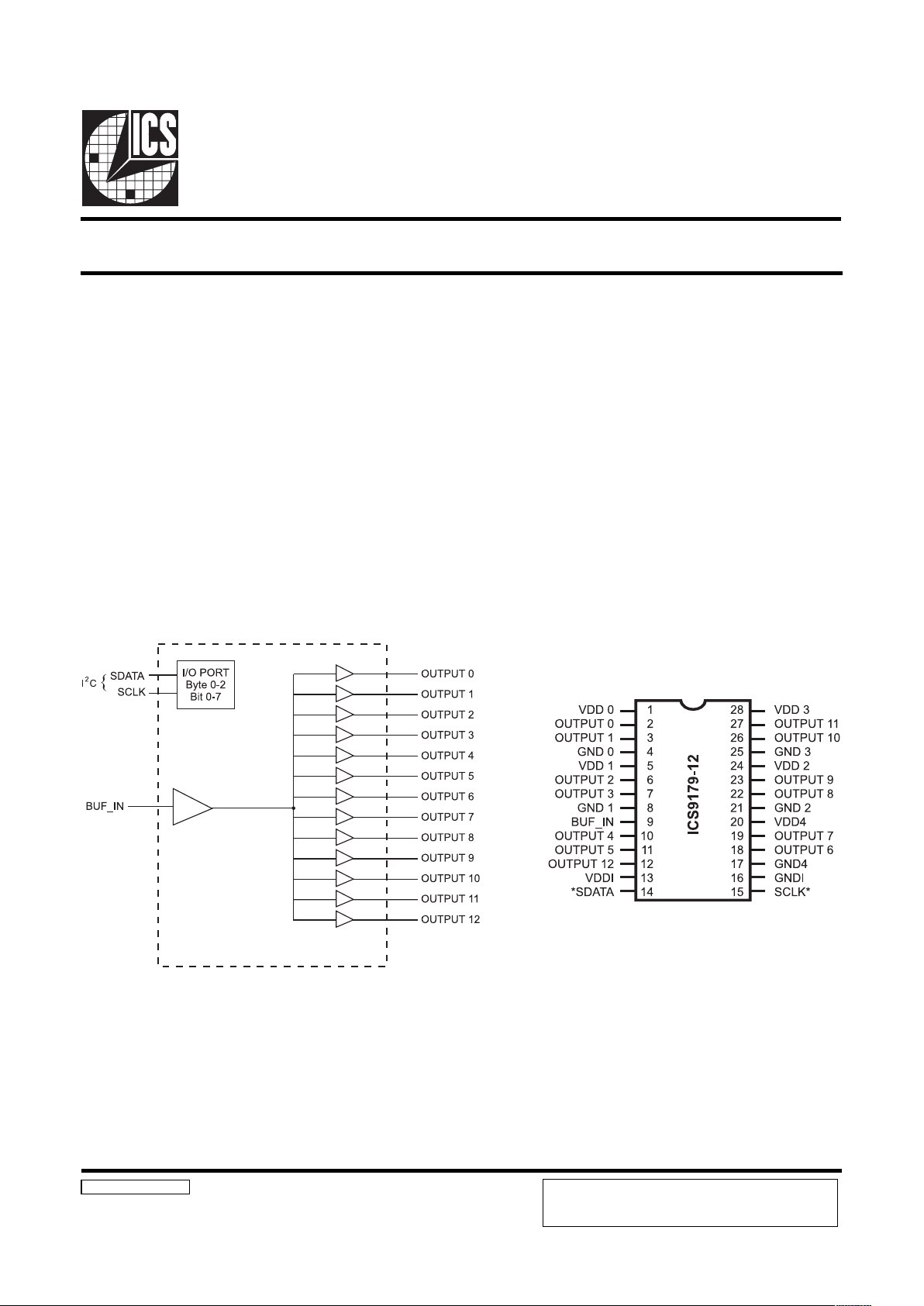
ICS9179-12
Block Diagram
PentiumPro is a trademark of Intel Corporation
I2C is a trademark of Philips Corporation
3 DIMM Buffer
9179-12 Rev C 7/16/99
Pin Configuration
The ICS9179-12 is a buffer intended for reduced pin count
2 - chip Intel BX chipset designs
An I2C interface is included, enabling individual outputs to be
turned on or off. With 13 outputs, up to 3 DIMMs are supported.
Thirteen high speed, low noise buffers, supports up to
three SDRAM DIMMs.
Buffer outputs skew matched to within 250ps.
I
2
C Serial Configuration interface to allow individual
OUTPUTs to be stopped low.
Multiple VDD, VSS pins for noise reduction
3.3V±5% supply voltage
28-pin SOIC and SSOP package
Propagation delay between 1 to 5.5ns
Operation to 133MHz at 3.3V±5%
28-Pin SOIC and SSOP
* Internal pull-up resistor of 100K
Ohms to 3.3V on indicated inputs
PRODUCT PREVIEW documents contain information on new
products in the sampling or preproduction phase of development.
Characteristic data and other specifications are subject to change
without notice.
Power Groups
VDD (0:4), GND (0:4) = Power supply for OUTPUT buffer
VDDI, GNDI = Power supply for I2C circuitry

2
ICS9179-12
Pin Descriptions
Notes:
1. At power up all thirteen OUTPUTs are enabled and active.
2. OE has a 100K Ohm internal pull-up resistor to keep all outputs active.
3. The SDATA and SCLK inputs both have internal pull-up resistors with values above 100K Ohms.
REBMUNNIPEMANNIPEPYTNOITPIRCSED
,11,01,7,6,3,2
,32,22,91,81,21
72,62
)21:0(TUPTUOTUOstuptuokcolC
1
9NI_FUBNIsreffubroftupnI
41ATADSO/IIrofnipataD
2
yrtiucricC
3
51KLCSO/IIrofnipkcolC
2
yrtiucricC
3
82,42,02,5,1)4:0(DDVRWPsreffubTUPTUOrofylppusrewoPV3.3
52,12,71,8,4)4:0(DNGRWPsreffubTUPTUOrofdnuorG
31IDDVRWPIrofylppusrewoPV3.3
2
cigollanretnidnayrtiucricC
61IDNGRWPIrofdnuorG
2
cigollanretnidnayrtiucricC

3
ICS9179-12
VDD
This is the power supply to the internal core logic of the
device as well as the clock output buffers for OUTPUT (0:12).
This pin operates at 3.3V volts. Clocks from the listed
buffers that it supplies will have a voltage swing from Ground
to this level. For the actual guaranteed high and low voltage
levels for the Clocks, please consult the DC parameter table
in this data sheet.
GND
This is the power supply ground (common or negative) return
pin for the internal core logic and all the output buffers.
OUTPUT (0:12)
These Output Clocks are use to drive Dynamic RAMs and
are low skew copies of the CPU Clocks. The voltage swing
of the OUTPUTs output is controlled by the supply voltage
that is applied to VDD of the device, operates at 3.3 volts.
I
2
C
The SDATA and SCLOCK Inputs are used to program the
device. The clock generator is a slave-receiver device in the
I2C protocol. It will allow read-back of the registers. See
configuration map for register functions. The I2C
specification in Philips I2C Peripherals Data Handbook
(1996) should be followed.
BUF_IN
Input for Fanout buffers (OUTPUT 0:12).
VDDI
This is the power supply to I2C circuitry.
T echnical Pin Function Descriptions
 Loading...