ICST AV9178Y-03, ICS9178Y-03 Datasheet

Integrated
Circuit
Systems, Inc.
General Description Features
ICS9178-03
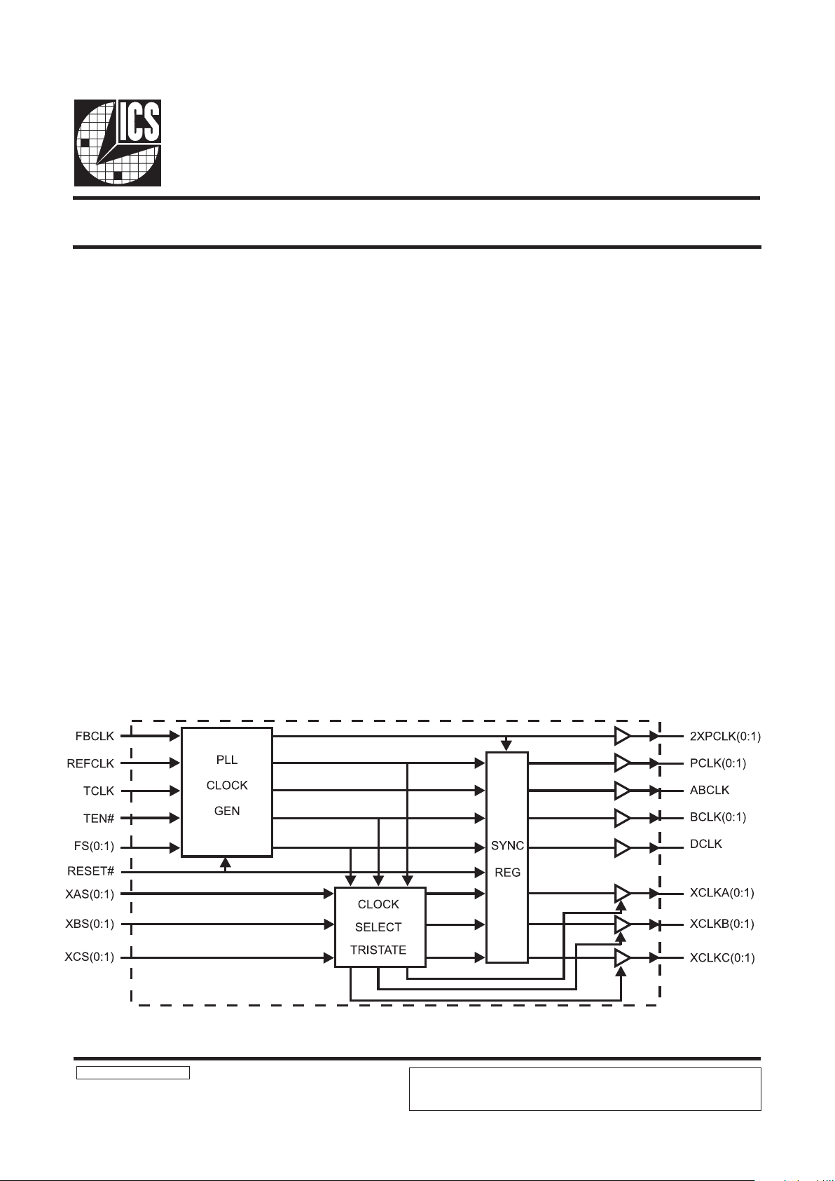
Block Diagram
ICS9178-03 Rev C 02/12/98P
245 MHz Clock Generator and Integrated Buffer for PowerPC
The ICS9178-03 generates all clocks required for high speed
PowerPC RISC microprocessor systems. Generating clocks
in phase with an external reference frequency allows the
ICS9178-03 to be used as a multiplying zero delay buffer.
Three different multiplying factors are externally selectable.
These factors can be customized for specific applications. An
external frequency can be directly applied to aid system
testing. With 2X processor clock speeds up to 245 MHz,
PECL outputs are provided. User selectable frequency ratios
are available for PCLK/BCLK and PCLK/XCLK. Each pair of
clocks outputs have separate supply pins to minimize output
jitter and allow them to operate at 5V, 3.3V or custom voltage
levels.
Generates 2 PECL 2x processor, 2 TTL/CMOS 1x
processor and 10 selectable bus clocks
2XPCLK ranges from 75 MHz to 245 MHz (5V or
5V/3.3V mixed supply) or 60 to 170 MHz (3.3V only)
Asymmetric duty cycle bus clock for PowerPC
Bus to processor clock skews less than ±250ps
2XPCLK to PCLK skew controlled at 300 ±300ps
Selectable reference multiplying factors
Selectable PCLK/BCLK and PCLK/XCLK ratios
Separate supplies allow 5V and 3.3V output mix
3.0V - 5.5V supply range
44-pin PQFP package
PowerPC is a trademark of Motorola Corporation.
Applications
Ideal for high-speed systems based on PowerPC
ICS reserves the right to make changes in the device data identified in this publication
without further notice. ICS advises its customers to obtain the latest version of all
device data to verify that any information being relied upon by the customer is current
and accurate.

2
ICS9178-03
Pin Configuration
44-Pin PQFP
*VCO range is limited from 75- 245 MHz at 5V ±5% and 60 - 170 MHz at 3.3V ±5%. Divide ratios assume BCLK is externally
fed back to FBCLK.
_=A,B,C
Functionality
The 2XPCLK series or Thevinen trace terminations must be optimized for the specific operating frequency and board
layout. The rising edge of ABCLK is coincident with the rising edges of 2XPCLK, PCLK and other BCLKs.
X_S1 X_S0 XCLK_(0,1)
00PCLK
0 1 BCLK
10DCLK
1 1 Tristate
FS1 FS0 RST TEN *VCO 2XPCLK PCLK ABCLK (H/L%) BCLK DCLK
00106x REFVCOVCO/2VCO/6 (66/33)VCO/6VCO/4
01108x REFVCOVCO/2VCO/8 (75/25)VCO/8VCO/4
10104x REFVCOVCO/2VCO/12 (50/50)VCO/4VCO/4
1110X11 1 11
XX0XX00000
0011TCLKTCLKTCLK/2TCLK/6 (66/33)TCLK/6TCLK/4
0111TCLKTCLKTCLK/2TCLK/8 (75/25)TCLK/8TCLK/4
1011TCLKTCLKTCLK/2TCLK/12 ( 66/33)TCLK/12TCLK/4
1111TCLKTCLKTCLK/2TCLK/2TCLK/2TCLK/4

3
ICS9178-03
Pin Description
*=Pin is pulled-up to VDD internally by the device.
PIN NUMBER PIN NAME TYPE DESCRIPTION
32 XAS0 Input LSB Programm able Group A frequency selector.
31 XAS1 Input MSB Program mable Group A frequency selector.
6 XCLKA0 Output TTL/CMOS group A programmable clock output.
5 XCLKA1 Output TTL/CMOS group A programmable clock output.
30 XBS0 Input LSB Programmable G roup B frequency selecto r.
29 XBS1 Input M SB Programmab le Group B frequen cy selector.
3 XCLK B0 O utput TTL /CMOS G roup B program mable clock output.
2 XCLK B1 O utput TTL /CMOS G roup B program mable clock output.
1 VDDXBA — Power for pro grammable Gro up A and B buffers (Pins 2, 3, 5, 6).
4 GNDXBA — Ground for programmable Group A and B buffers (Pins 2, 3, 5, 6).
44 GNDXC — Ground for the programmable Group C buffers (Pins 42 and 43).
43 XCLKC 0 Ou tput TTL /CMOS Grou p C programm able clock output.
42 XCLKC 1 Ou tput TTL /CMOS Grou p C programm able clock output.
41 VDDXC — Power for the XC signal output buffers (Pins 42 and 43).
28 XCS0 Input LSB Programmable G roup C frequency selecto r.
27 XCS1 Input M SB Programmab le Group C frequen cy selector.
11 PCLK0 Output TTL/CMOS 1X Processor clock ou tput.
10 PCLK1 Output TTL/CMOS 1X Processor clock ou tput.
8 GNDP — Ground for PCLK output buffers (Pins 11 and 10).
7 VDDP — Power for PCLK output buffers (Pins 11 and 10).
22 2XPCLK0 Output PECL 2X Processor clock output.
21 2XPCLK1 Output PECL 2X Processor clock output.
24 EVDD — Power for PECL buffers (Pins 21 and 22 ).
23 EGND — Ground for PECL buffers (Pins 21 and 2 2).
20 EGND — Ground for PECL buffers (Pins 21 and 2 2).
38* FS0 Input LSB frequency select PLL (divider mode control).
37* FS1 Input MSB frequenc y select PLL (divider mode control).
36 FBCLK Input External PLL feedback path from one of the BCLK outputs.
35 REFCLK Input Extern al reference clock input.
25 AVDD — Power for the analog PLL circuitry.
26 AGND — Ground for the analog PLL circuitry.
19 DCLK Output TTL/CMOS D clock output.
16 VDDD — Power for D output buffers (Pin 19).
17 GNDD — Ground for D output buffer (Pin 19).
15 BCLK0 Output TTL/CMOS B (Bus) clock output.
14 BCLK1 Output TTL/CMOS B (Bus) clock output.
13 GNDBAB — Ground for output buffers AB and B clocks (Pins 14, 15 & 18).
12 VDDBAB — Power for output buffers AB and B clocks (Pins 14, 15 & 18).
18 ABCLK Output TTL/CMOS AB Bus clock (has Asymmetric duty cycle).
40 TCLK Input External test clock input.
39 TEN# Input Test enable (tie low).
9 RESET # Input Sy nc register reset (active low).
33 VDD — Digital power s upply for 5.0 or 3.3V.
34 GND — Digital ground s upply.
 Loading...