

ICST AV9173-15CS08, AV9173-15CN08, ICS9173-15CN08, ICS9173-15CS08 Datasheet
Integrated
Circuit
Systems, Inc.
General Description Features
AV9173-15
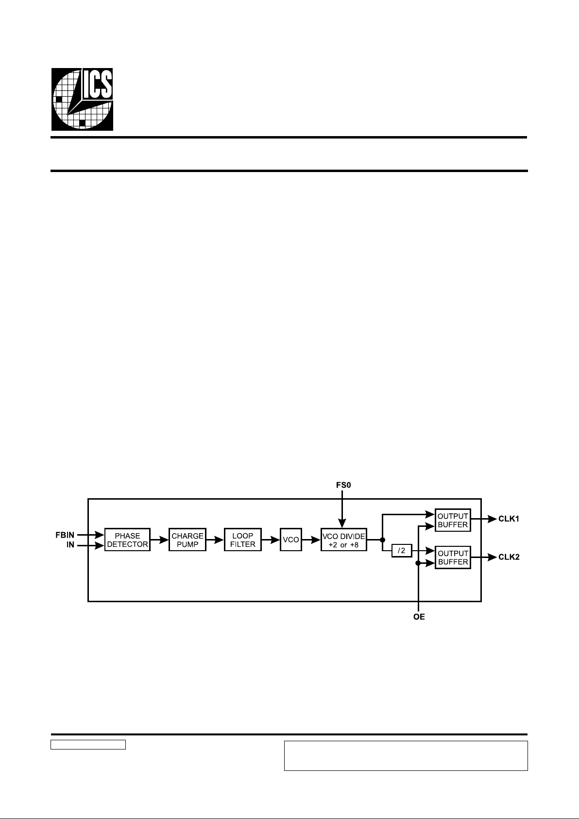
Block Diagram
Video Genlock PLL
AV9173-15RevC051397P
• Phase-detector/VCO circuit block
• Ideal for genlock system
• Reference clock range 12 kHz to 1 MHz
(see specification of output clock range)
• Output clock range 0.625 to 37.5 MHz for CLK1,
depending on input conditions (see Table 1) on page 2.
• Provides h-sync capability with CLK1 outputs
15 to 37.5 MHz for 15kHz input
• On-chip loop filter
• Single 5 volt power supply
• Low power CMOS technology
• Small 8-pin DIP or SOIC package
The AV9173-15 provides the analog circuit blocks required
for implementing a video genlock dot (pixel) clock
generator. It contains a phase detector, charge pump, loop
filter, and voltage-controlled oscillator (VCO). By grouping
these critical analog blocks into one IC and utilizing
external digital functions, performance and design
flexibility are optimized as are development time and
system cost.
When used with an external clock divider, the AV9173-15
forms a Phase-Locked Loop configured as a frequency
synthesizer. The AV9173-15 is designed to accept video
horizontal synchronization (h-sync) pulses and produce a
video dot clock. A separated, negative-going sync input
reference pulse is required at pin 2 (IN).
The AV9173-15 is also suited for other clock recovery
applications in such areas as data communications.
ICS reserves the right to make changes in the device data identified in this
publication without further notice. ICS advises its customers to obtain the latest
version of all device data to verify that any information being relied upon by the
customer is current and accurate.
2
AV9173-15
Pin Descriptions
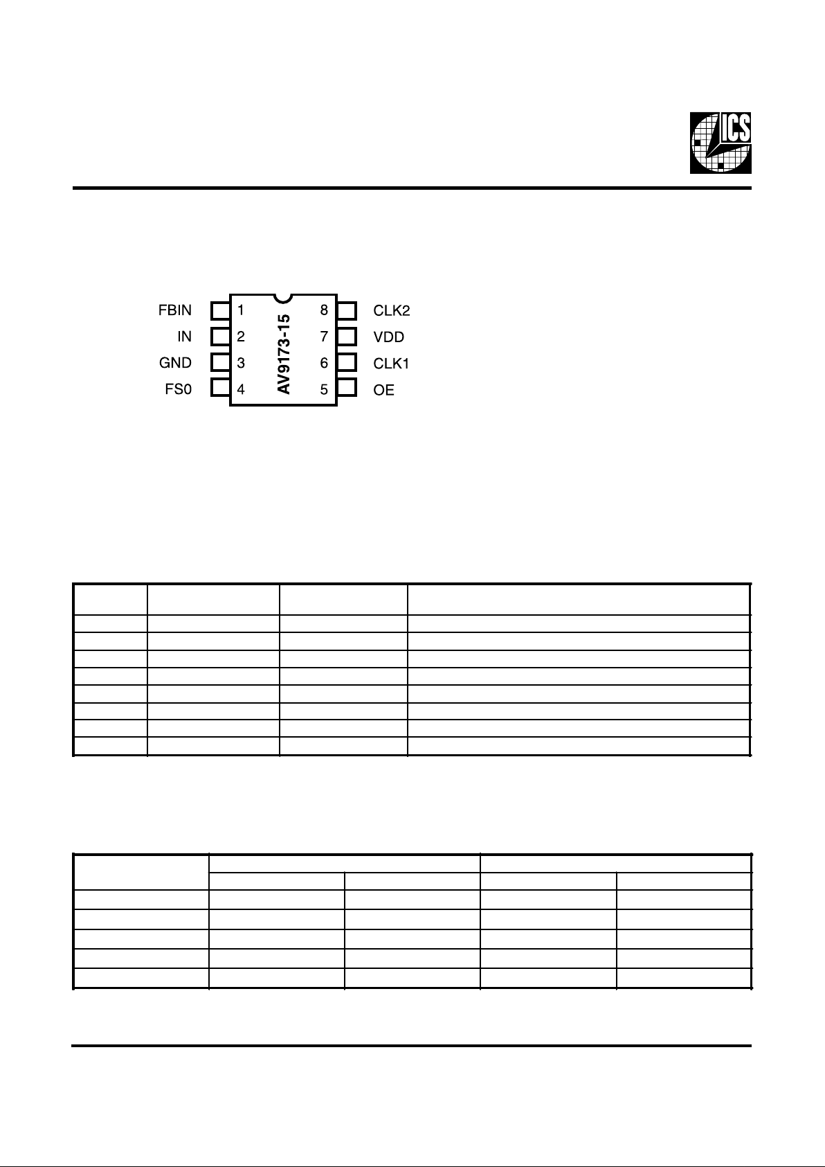
Pin Configuration
8-Pin DIP or SOIC
Table 1: Allowable Input Frequency to Output Frequency
(Outputs in MHz)
PIN
NUMB ER
PIN NAME TYPE DESCRIPTION
1 FBIN Inp ut Feedback Input
2
IN Inp ut Input for reference sync pulse
3 GND — Ground
4 FS0 Inp ut Internal VCO divider select input
5 OE Inp u t Output E nable
6 CLK1 Out put Clock Output 1
7 VDD — Power Supply (+5V)
8 CLK2 Out pu t Cloc k Output 2 (Divided-by-2 from Clock 1)
fIN (kHz)
f
OUT for FS = 0 (M Hz) fOUT for FS = 1 (MHz)
CL K1 Ou tp ut CL K2 O utp u t CL K1 O utp u t CL K2 O u tpu t
12
≤ fIN ≤ 14 kHz
22.0 to 37.5 11.0 to 18.75 5.5 to 9.375 2.75 to 4.6875
14
< fIN ≤ 17 kHz
15 to 37.5 7.5 to 18.75 3.75 to 9.375 1.875 to 4.6875
17
< fIN ≤ 30 kHz
12.5 to 37.5 6.25 to 18.75 3.125 to 9. 375 1.5625 to 4.6875
30
< fIN ≤ 35 kHz
7.5 to 37.5 3.75 to 18.75 1.875 to 9. 375
0.9375 to 4. 6875
35
< fIN ≤ 1000 kHz
5.0 to 37.5 2.5 to 18.75
1.25 to 9.375 0.625 to 4.6875
 Loading...