ICST AV9169CF-46, ICS9169CF-46 Datasheet

Integrated
Circuit
Systems, Inc.
General Description Features
ICS9169C-46
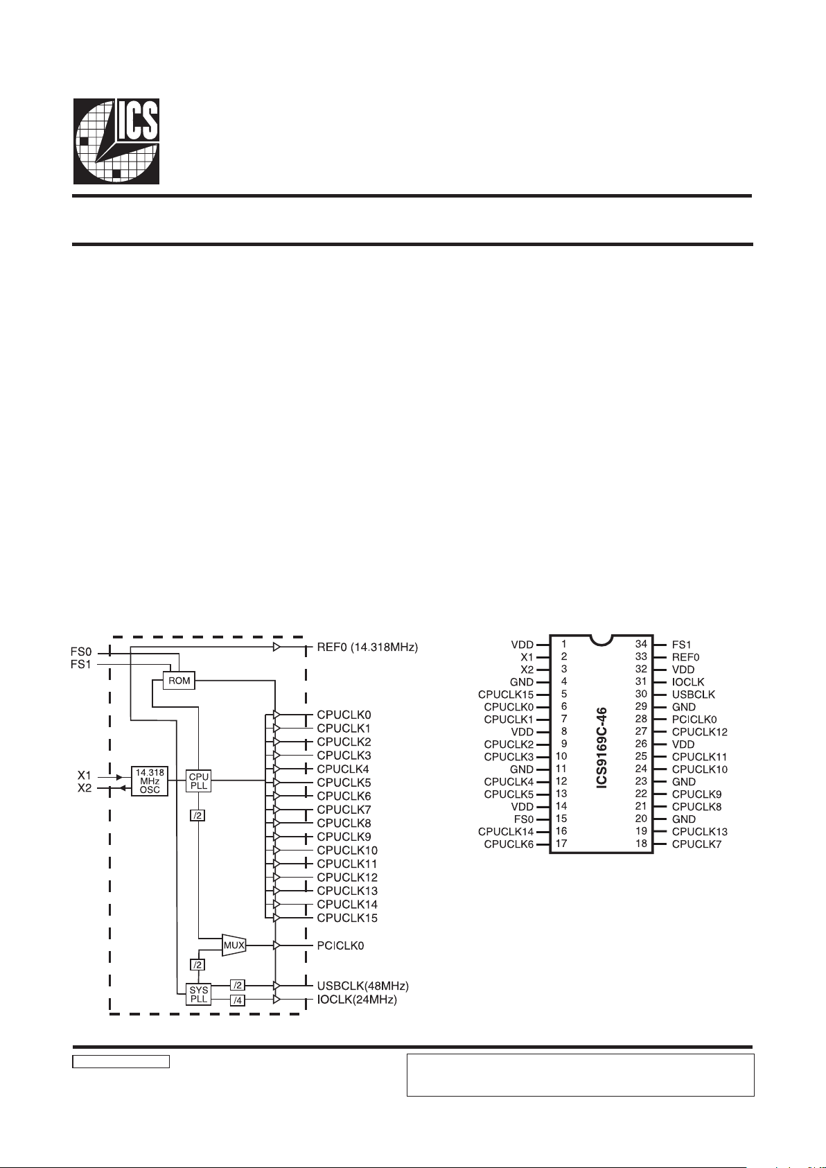
Block Diagram
Frequency Generator for PentiumPro Based Systems
9169C-46RevA072597P
Pin Configuration
34-Pin SSOP
Pentium is a trademark on Intel Corporation.
16 selectable CPU clocks up to 66.66 MHz
One synchronous PCI clock.
One USB clock at 48MHz, meets Intel jitter,
accuracy, as well as rise and fall time requirements
One I/O clock at 24MHz
One Ref. Clock at 14.318MHz
CPU clocks to PCI clock skew of 1-4ns (CPU early)
Low CPU and PCI clock jitter <200ps
Low skew outputs, skew window 250ps for CPU
clocks and for PCI clocks
Improved output drivers are designed for low EMI
Test Mode
3.3V ±10% operation
Space saving and low cost 34-pin SSOP package
The ICS9169C-46 is a Clock Synthesize/Driver chip for
Pentium, PentiumPro or Cyrix 68x86 based motherboards
using SDRAM.
Features include sixteen CPU outputs, twelve of which can
be used to support up to three SDRAM modules. The
PCICLK output can be buffered with an external, low cost
zero delay buffer. Additionally, the device meets the
Pentium and PentiumPro power-up stabilization, which
requires that CPU and PCI clocks be stable within 2ms after
power-up.
The ICS9169C-46 clock outputs are designed for low EMI
emissions. Controlled rise and fall times, unique output
driver circuits and innovative circuit layout techniques enable
the ICS9169C-46 to have lower EMI than other clock
devices.
The ICS9169C-46 accepts a 14.318MHz reference crystal
or clock as its input and runs from a 3.3V supply.
ICS reserves the right to make changes in the device data identified in this
publication without further notice. ICS advises its customers to obtain the latest
version of all device data to verify that any information being relied upon by the
customer is current and accurate.

2
ICS9169C-46
Pin Descriptions
Functionality
3.3V±10%, 0-70°C
Crystal (X1, X2) = 14.31818 MHz
FS1 FS0 XTALIN
CPUCLK (0: 15)
(MHz)
PCICLK0
(MHz)
REF(0:1)
(MHz)
USBCLK
(MHz)
IOCLK
(MHz)
0 0 14.318MHz Hi-Z Hi-Z Hi-Z Hi-Z Hi-Z
0 1 14.318MHz 66.67 33.3 14.318 48 24
1 0 14.318MHz 50.0 25.0 14.318 48 24
1 1 14.318MHz 60.0 30.0 14.318 48 24
Actual Output Frequencies
Output Clocks
Target Frequency
(MHz)
Actual Frequency
(MHz)
CPUCLK (0:15) 50.0 48.83
CPUCLK (0:15) 60.0 60.0
CPUCLK (0:15) 66.67 68.66
USBCLK 48 48.008
IOCLK 24 24.004
PIN NUMBER PIN NAME TYPE DESCRIPTION
1, 8, 14, 26, 32 V
DD
PWR Voltage Supply
2 X1 IN Reference crystal input
3 X2 OUT Reference crystal feedbac k
4, 11 20, 23, 29 GND PWR Ground
5, 6, 7, 9, 10, 12,
13, 16, 17, 18, 19,
21, 22, 24, 25, 27
CPUCLK(0:15) OUT CPU clock outputs
15, 34 FS (0:1) IN CPU clock select input bits. These devices have internal pull-ups
28 PCICLK OUT BUS cl ock output
30 USBCLK OUT USB clock out put 48 MHz
31 IOCLK OUT I/O cloc k output 24 MHz
33 REF0 OUT Reference clock output (14.318 MHz)
 Loading...