ICST AV9169CF-26, ICS9169CF-26 Datasheet

Integrated
Circuit
Systems, Inc.
General Description Features
ICS9169C-26
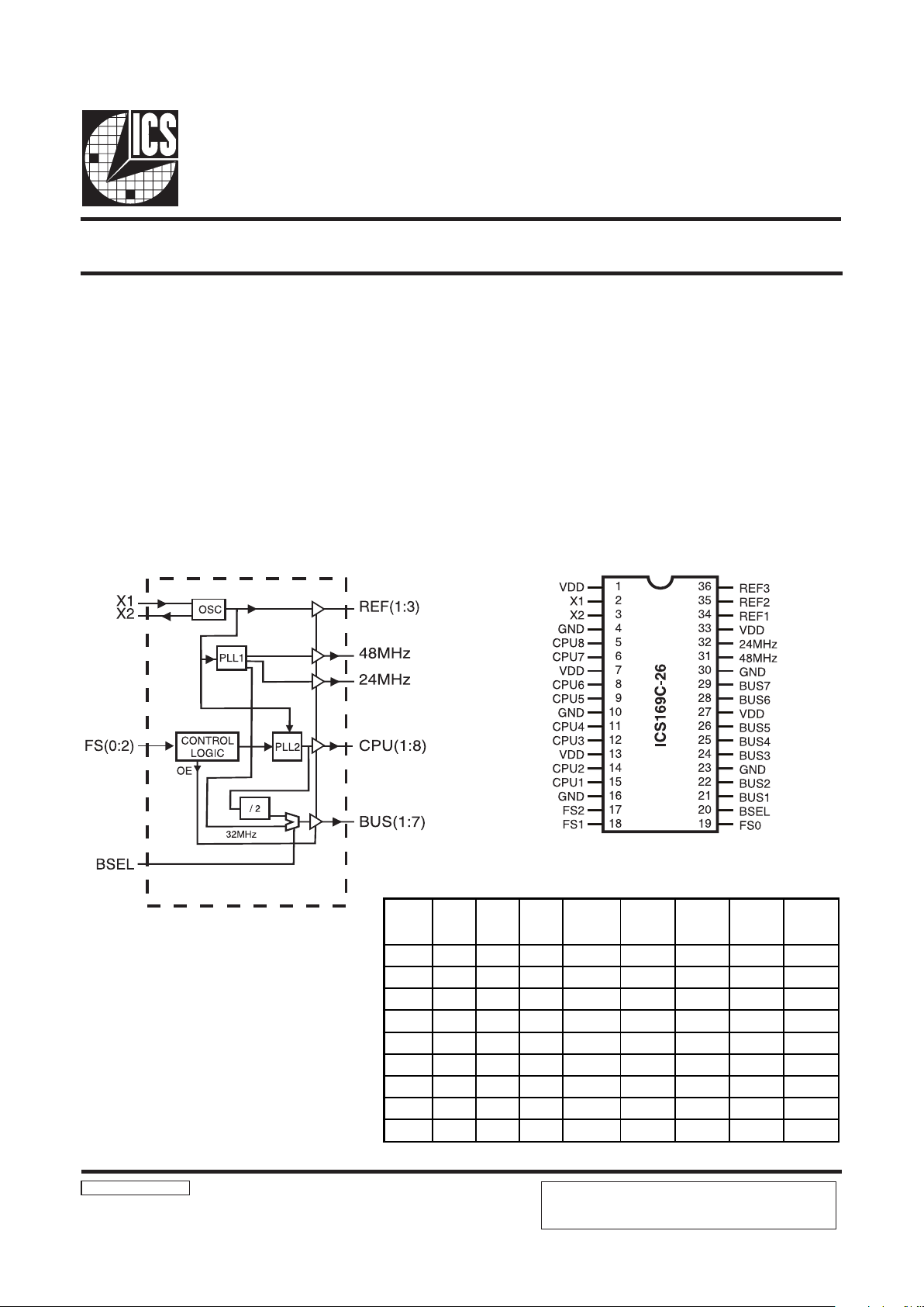
Block Diagram
Frequency Generator and Integrated Buffers
9169C-26RevB091997P
Pin Configuration
Twelve selectable CPU clocks operate up to 83.3 MHZ
Eight selectable CPU clocks operate up to100 MHz
Maximum CPU jitter of ±200ps
Seven BUS clocks support sync or async bus operation
500ps skew window for all synchronous clock edges
CPU clocks to BUS clocks in sync mode skew
1-4ns (CPU early)
Integrated buffer outputs drive up to 30pF loads
3.0V - 3.7V supply range
36-pin SSOP package
48 MHz clock for USB support and 24 MHz clock for FD
36-Pin SSOP
Functionality
3.3V±10%, 0-70°C
Crystal (X1, X2) = 14.31818 MHz
Pentium is a trademark on Intel Corporation.
The ICS9169C-26 is a low-cost frequency generator
designe specifically for Pentium-based chip set systems.
The integrated buffer minimizes skew and provides all the
clocks required. A 14.318 MHz XTAL oscillator provides
the reference clock to generate standard Pentium
frequencies. The CPU clock makes gradual frequency
transitions without violating the PLL timing of internal
microprocessor clock multipliers.
Either synchronous (CPU/2) or asynchronous (32 MHz)
PCI bus operation can be selected.
BSEL FS2 FS1 FS0
CPU
(1:8)
MHz
BUS
(0:7)
MHz
48 MHz 24 MHz
REF
(1:3)
0 0 0 0 55 27.5 48 24 14.318
0 0 0 1 80 40 48 24 14.318
0 0 1 0 100 50 48 24 14.318
0 0 1 1 75 37.5 48 24 14.318
0 1 0 0 50 25 48 24 14.318
0 1 0 1 66.6 33.3 48 24 14.318
0 1 1 0 60 30.0 48 24 14.318
0 1 1 1 Tristate Tristate Tristate Tristate Tristate
1 select select select Tristate 32.0 48 24 14.318
PRODUCT PREVIEW documents contain information on new
products in the sampling or preproduction phase of development.
Characteristic data and other specifications are subject to change
without notice.
Preliminary Product Preview

2
ICS169C-26
Preliminary Product Preview
Pin Descriptions
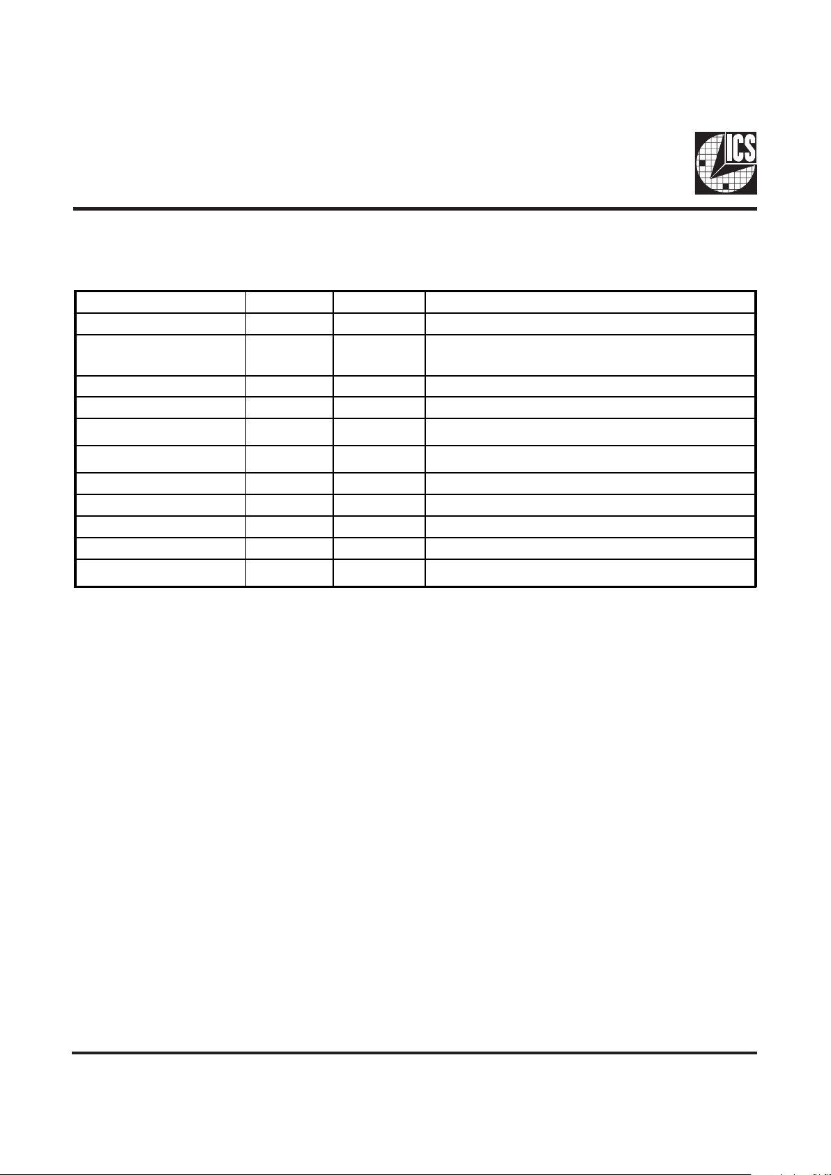
PIN NUMBER PIN NAME TYPE DESCRIPTION
1, 7, 13, 27, 33 VDD PWR Power for contr ol logic, PLL and o utput buffers.
2X1IN
XTAL or external reference frequency input. This input
includes XTAL load capacitance and feedback bias for a 12 16 MHz crystal, nominally 14. 31818 Mhz.
3 X2 OUT XTAL output which includes XTAL load capacitance.
4, 10, 16, 23, 30 GND PWR Ground for logic, PLL and output buffers.
5, 6, 8, 9, 11, 12, 14, 15 CPU(1:8) OUT
Processor clock outputs which are a multiple of the input
reference frequency as shown in the table above.
17, 18, 19 FS(1:2) IN
Frequency mult iplier select pi ns. See table a bove. These input s
have interna l pull-up device s.
20 BSEL IN Selector for sy nchronous or asyn chronous bus op eration.
21, 22, 24, 2 5, 26, 28, 29 BUS(1:7) OUT Bus c lock outputs.
31 48MHz OU T Fixed 48 M Hz clock (wit h 14.318 MHz i nput).
32 24MHz OU T Fixed 24 M Hz clock (wit h 14.318 MHz i nput).
34, 35, 36 REF(1:3) OUT
REF is a buffered copy of the crystal oscillator or reference
input clock, nominally 14.31818 Mhz.
 Loading...