ICST AV9169AM-70 Datasheet

Integrated
Circuit
Systems, Inc.
General Description Features
ICS9169A-70
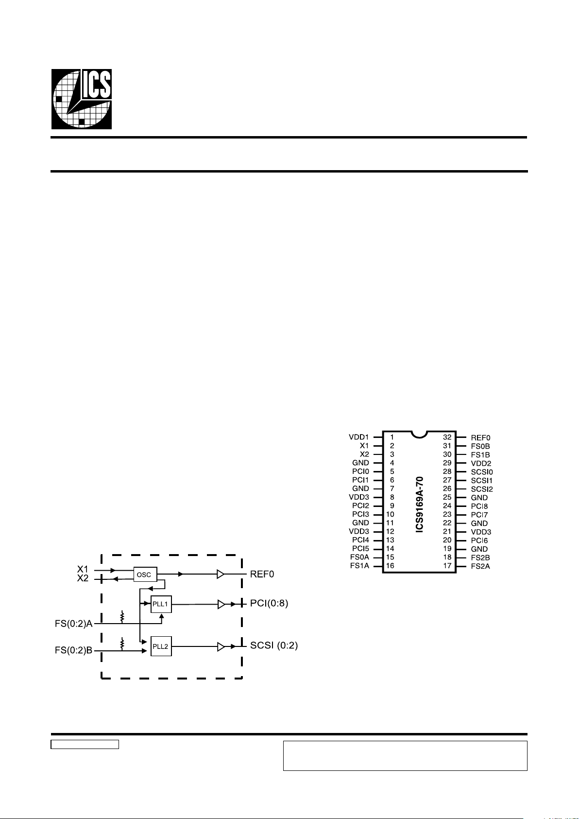
Block Diagram
Frequency Generator for Workstation Systems
9169A-70 Rev B 2/14/01
Pin Configuration
32-Pin SOIC
• 9 PCI outputs selectable from 30 to 66.6MHz
• 3 SCSI outputs, selectable from 10 to 80MHz
• 500ps skew window for all synchronous clock edges
• Integrated buffer outputs drive up to 30pF loads
• 500ps output to output skew window
• Buffers drive 30pF loads nominally 0.8V/ns skew rate
• 3.0V - 3.7Vsupply range
• 32-pin SOIC package
• 48 MHz clock for USB support and 24 MHz clock
for FD
The ICS9169A-70 is a low-cost frequency generator designed
specifically for workstation or PC system clocks. The
integrated buffer minimizes skew and provides all the clocks
required. A 14.318 MHz XTAL oscillator provides the
reference clock to generate standard Pentium frequencies.
The CPU clock makes gradual frequency transitions without
violating the PLL timing of internal microprocessor clock
multipliers.
ICS reserves the right to make changes in the device data identified in this
publication without further notice. ICS advises its customers to obtain the latest
version of all device data to verify that any information being relied upon by the
customer is current and accurate.

2
ICS9169A-70
Pin Descriptions
REBMUNNIPEMANNIPEPYTNOITPIRCSED
11DDVRWP.sreffubtuptuodnaLLP,cigolrofrewoP
21XNI
sihT.tupniycneuqerfecnereferlanretxeroLATX
kcabdeefdnaecnaticapacdaolLATXsedulcnitupni
81813.41yllanimon,latsyrczHM61-21arofsaib
.zhM
32XTUO
daolLATXsedulcnihcihwtuptuoLATX
.ecnaticapac
42,32,02,41,31,01,9,6,5)8:0(ICPTUOstuptuokcolcICP
52,22,91,11,7,4DNGRWP.sreffubtuptuodnaLLP,cigolrofdnuorG
12,21,83DDVRWPstuptuokcolcICProfrewoP
71,61,51A)2:0(SFNI
.evobaelbateeS.sniptcelesreilpitlumycneuqerF
.secivedpulluplanretnievahstupniesehT
922DDVRWPstuptuokcolcISCSrofrewoP
62,72,82)2:0(ISCSTUOstuptuokcolcISCS
81,03,13B)2:0(SFNI
txenelbateeS.sniptcelesreilpitlumycneuqerF
secivedpulluplanretnievahstupniesehT.egap
230FERTUO
rorotallicsolatsyrcehtfoypocdereffubasiFER
.zHM81813.41yllanimon,kcolctupniecnerefer
Note:
X1, X2 contain iternal 18pF crystal load cap. Intended to have external load
caps of 15 to 18pF required for nominal crystal of 17 to 18pF crystal total load.

3
ICS9169A-70
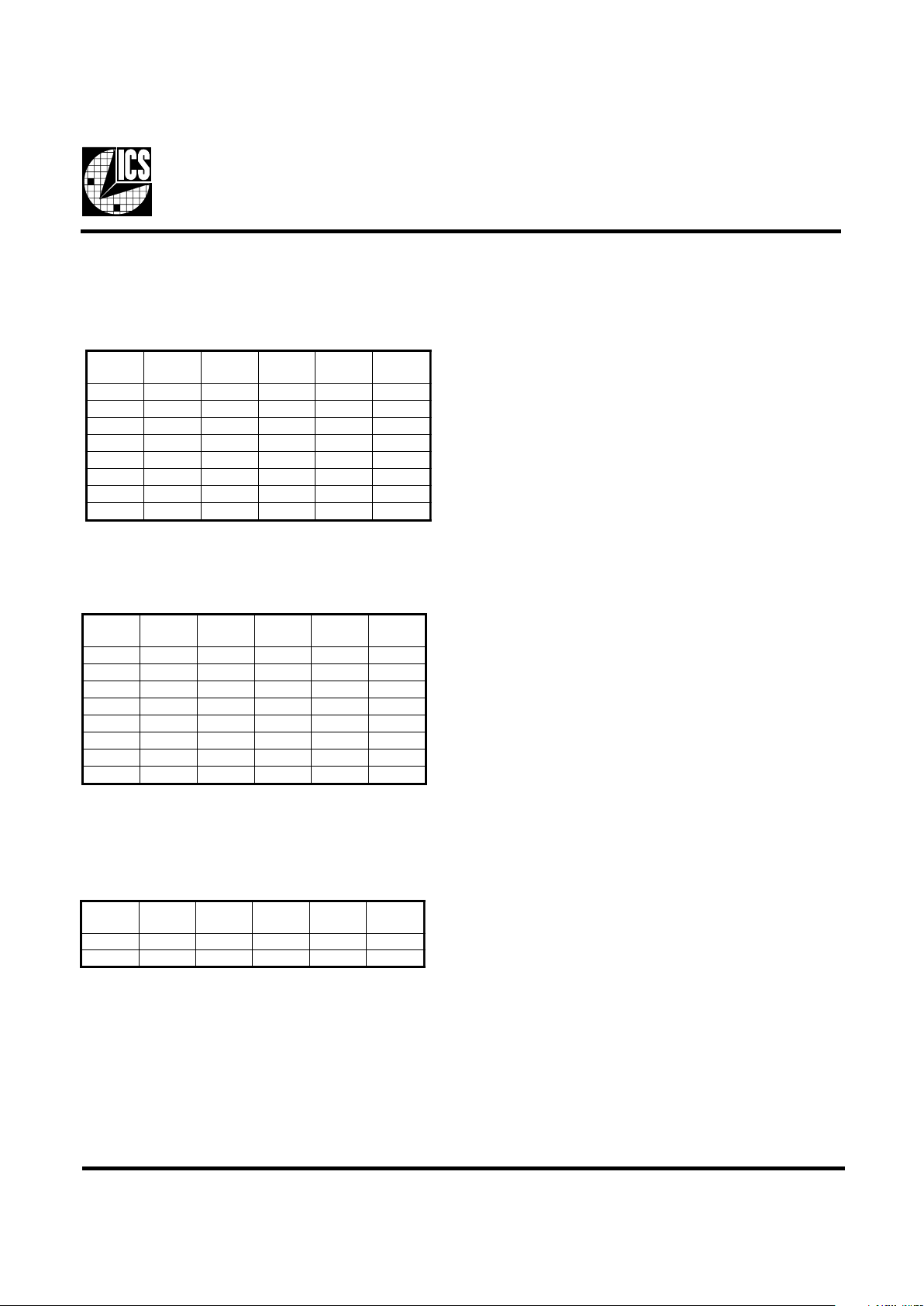
B2SFB1SFB0SF
tegraT
zHM
lautcA
zHM
FER
zHM
000 4242813.41
0018470.84813.41
010 0120.01813.41
0110250.02813.41
100 0490.04813.41
101 0511.05813.41
110 0641.06813.41
1110881.08813.41
A2SFA1SFA0SF
tegraT
zHM
lautcA
zHM
FER
zHM
000 etatsirTetatsirTetatsirT
001 2/FER2/FERFER
010 0370.03813.41
011 3.3372.33813.41
100 0511.05813.41
101 5598.45813.41
110 0641.06813.41
111 6.6636.66813.41
SCSI outputs: SCSI(0:2)
(Assume divide by 2 from VCO)
PCI outputs: PCI (0:8)
(Assume divide by 2 from VCO)
VDD = 3.3±10%, TA = 0 to 70°C
Crystal = 14.31818MHz
Note: When FS(0:2)A is 000 or 001, the Tristate and
Test modes applies to all outputs for REF, PCI, and
SCSI outputs.
Note: 1. In T est mode, each PLL is bypassed. The clock
signal at X1 (externally driven clock or the
crystal) is applied to the divider circuits.
A2SFA1SFA0SFICPISCS
FER
000 etatsirTetatsirTetatsirT
001 2/FER
1
2/FER
1
FER
1
 Loading...