ICST AV9158-03CW24, ICS9158-03CW24 Datasheet

Integrated
Circuit
Systems, Inc.
General Description Features
ICS91 58-03
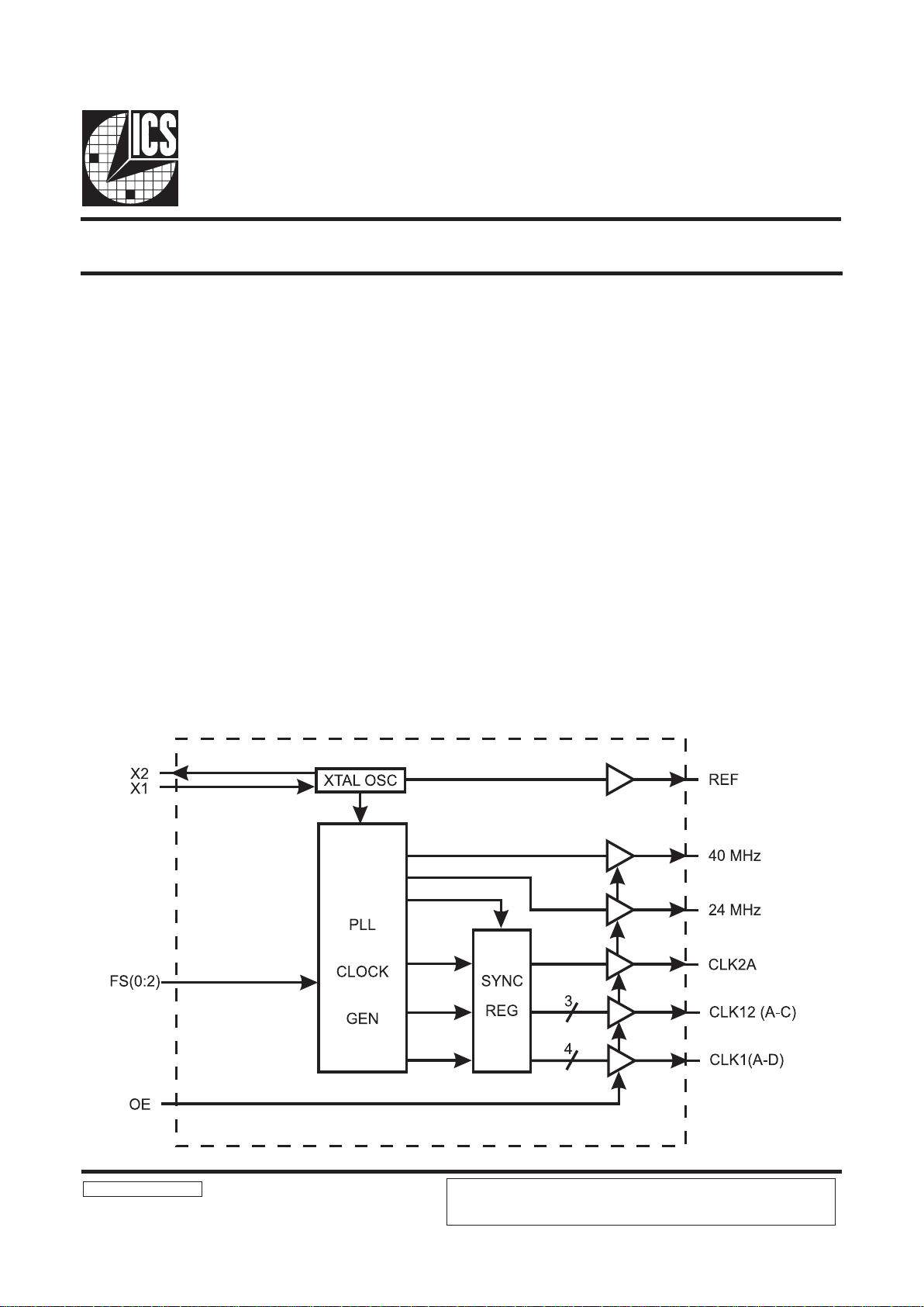
Block Diagram
9158-03 Rev D 7/28/98
Applications
Frequency Generator and Integrated Buffer
The ICS9158-03 is a low-cost frequency generator designed
specifically for desktop and notebook PC applications. Eight
copies of the CPU clock are available.
Each high drive (40mA) output is capable for driving a 30pF
load and has a typical duty cycle of 50/50. The clock
outputs are skew-controlled to within ±250ps.
The ICS9158-03 makes a gradual transition between
frequencies, so that it meets the Intel cycle-to-cycle timing
specification for 486 and Pentium systems.
8 skew-free, high drive CPU/BUS clocks
Up to 100 MHz output
±250ps skew between all outputs
Outputs can drive up to 30pF load and 40mA
50±10% duty cycle
Compatible with 486 and Pentium CPUs
On-chip loop filter components
4.5V - 5.5V supply range
24-pin SOIC package
Ideal for RISC or CISC systems such as 486, Pentium,
PowerPC, etc. requiring multiple CPU and BUS
clocks.
ICS reserves the right to make changes in the device data identified in this publication
without further notice. ICS advises its customers to obtain the latest version of all
device data to verify that any information being relied upon by the customer is current
and accurate.

2
ICS9158-03
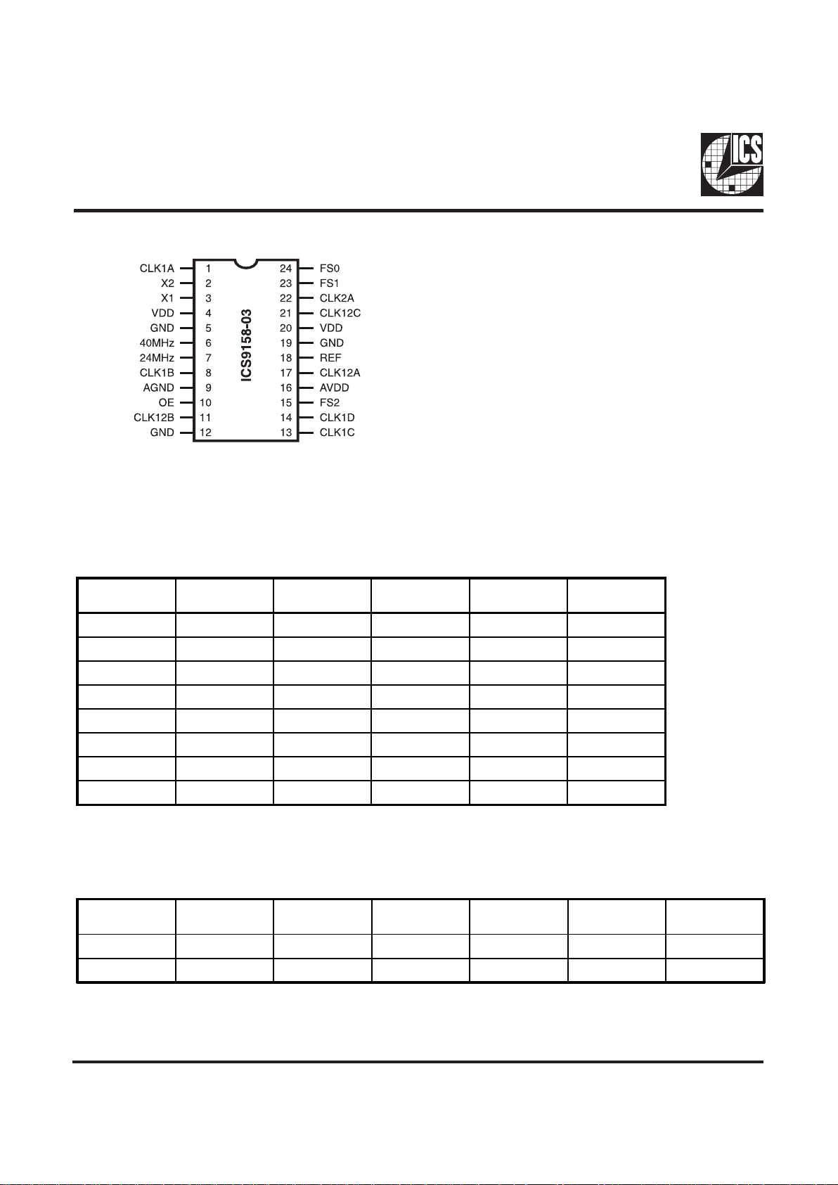
Pin Configuration
24-Pin SOIC
Functionality
(Assuming 14.318 MHz input.)
VDD=5V±10% or 3.3V±10%, TEMP=0-70°C
Peripheral Clocks
FS2 FS1 FS0
CLK2 A
(MHz )
CLK1 2(A -C)
(MHZ )
CL K1( A-D )
(MHz)
000321616
001323216
010321616
011323216
1 0 0 502525
1 0 1505025
1 1 0 66.67 33.33 33.33
1 1 1 60 60 30
OE C L K2A CL K12 (A -C) CL K12 (A -D )
40MHz
(Pin 6 )
24MHz
(Pin 7 )
REF
(Pin 1 8)
1 Runs Runs Runs 39.92 23.95 14.31818
0 TristateTristateTristateTristateTristateTristate

3
ICS9158-03
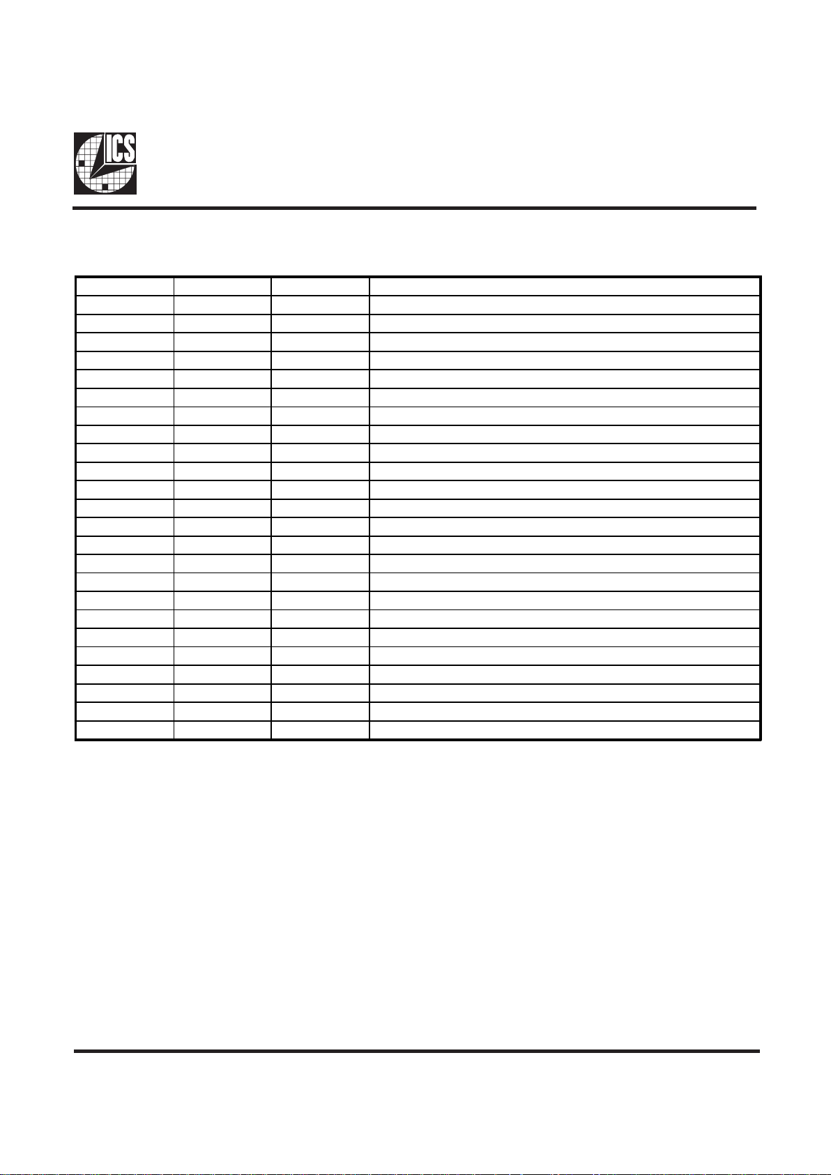
Pin Descriptions for ICS9158-03
PIN NUMBER PIN NAME TYPE DESCRIPTION
1 CLK1A OUT CLK1A clock output
2 X2 OUT Crystal connection
3 X1 IN Crystal connection
4 VDD PWR Digital POWER SUP PLY (+5V)
5 GND PWR Digital GROUND
6 40 M Hz OUT 40 M Hz clock output
7 24 M Hz OUT 24 M Hz floppy disk/combination I/O clock output
8 CLK1B OU T CLK1B clock output
9 AGND PW R ANALOG GROUND
10 OE IN OUTPUT ENABLE. Tristates all outputs when low.
11 CL K12B OUT CLK 12B clock output
12 GND PWR Digital GROUND
13 CLK 1C OUT CLK1C clock output
14 CLK1D OUT CLK1D clock output
15 F S2 IN CPU clock frequ ency select 2
16 AVDD PW R ANALOG power supply (+5V)
17 CLK 12A OUT CLK12A clock output
18 RE F OUT 14.31818 MHz clock output
19 GND PWR Digital GROUND
20 VDD PW R Digital POW ER SU PPLY (+5V )
21 CL K12C OU T 2X CPU clock output
22 CLK2A OUT CPU clock output
23 FS1 IN CPU clock frequency select 1
24 FS0 IN CPU clock frequency select 0
 Loading...