

ICST AV9155C-36CN20, AV9155C-36CM20, AV9155C-23CN20, AV9155C-23CM20, AV9155C-02CN20 Datasheet
...
Integrated
Circuit
Systems, Inc.
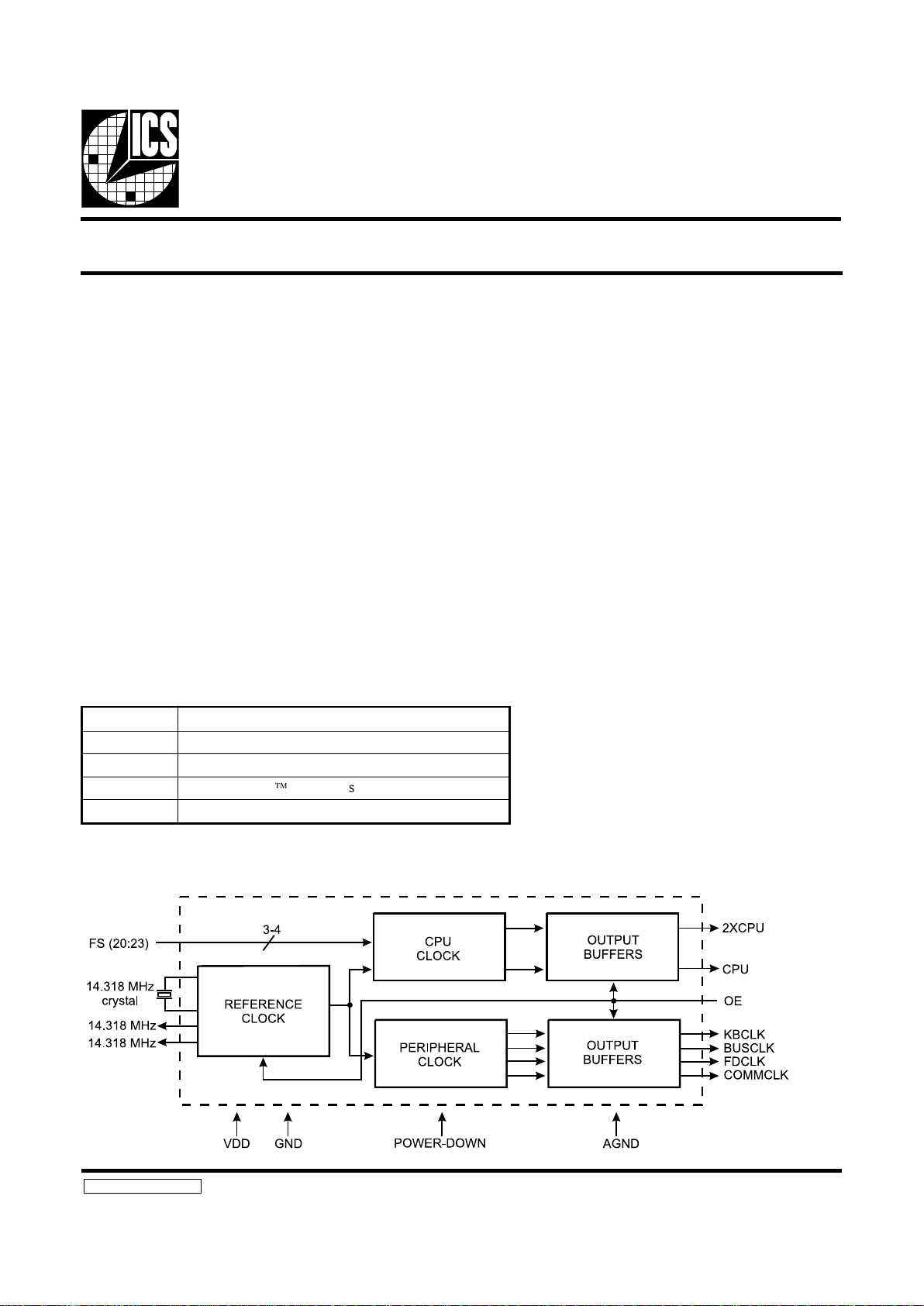
General Description Features
AV9155C
Block Diagram
AV9155C Rev F 12/13/00
Low Cost 20-Pin Frequency Generator
The AV9155C is a low cost frequency generator designed
specifically for desktop and notebook PC applications with
either 3.3V or 5.0V power supply voltage. Its CPU clocks
provide all necessary CPU frequencies for 286, 386 and 486
systems, including support for the latest speeds of processors.
The device uses a 14.318 MHz crystal to generate the CPU
and all peripheral clocks for integrated desktop motherboards.
The dual 14.318 MHz clock outputs allows one output for the
system and one to be the input to an ICS graphics frequency
generator such as the AV9194.
The CPU clock offers the unique feature of smooth, glitchfree transitions from one frequency to the next, making this
ideal device to use whenever slowing the CPU speed. The
AV9155C makes a gradual transition between frequencies, so
that it obeys the Intel cycle-to-cycle timing specification for
486 systems. The simultaneous 2X and 1X CPU clocks offer
controlled skew to within 1.5ns (max) of each other.
ICS offers several versions of the AV9155C. The different
devices are shown below:
• Compatible with 286, 386, and 486 CPUs
• Supports turbo modes
• Generates communications clock, keyboard clock,
floppy disk clock, system reference clock, bus clock
and CPU clock
• Output enable tristates outputs
• Up to 100 MHz at 5V or 3.3V
• 20-pin DIP or SOIC
• All loop filter components internal
• Skew-controlled 2X and 1X CPU clocks
• Power-down option
ICS has been shipping motherboard frequency generators
since April 1990, and is the leader in the area of multiple
output clocks on a single chip. The AV9155C is a third
generation device, and uses ICS’s patented analog CMOS
phase-locked loop technology for low phase jitter. ICS of fers
a broad family of frequency generators for motherboards,
graphics and other applications, including cost-effective
versions with only one or two output clocks. Consult ICS for
all of your clock generation needs.
Pentium is a trademark of Intel Corporation.
TRAPNOITPIRCSED
10-C5519VAKLCSUBzHM61htiwrotarenegkcolcdraobrehtoM
20-C5519VAKLCSUBzHM23htiwrotarenegkcolcdraobrehtoM
32-C5519VAmuitnePsedulcnI
Ô
seicneuqerf
63-C5519VAkcolcISCSzHM04laicepsaserutaeF
2
A V9155C
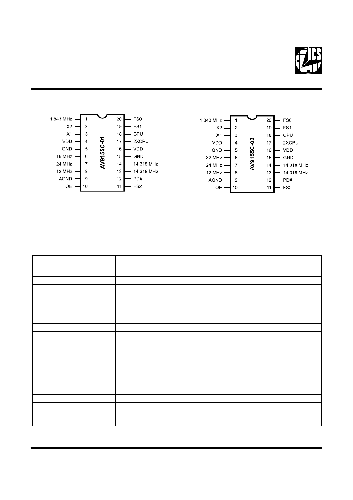
Pin Configuration
20-Pin DIP or SOIC
20-Pin DIP or SOIC
Pin Descriptions for A V9155C-01, -02
NIP
REBMUN
EMANNIPEPYTNOITPIRCSED
1zHM348.1tuptuO.tuptuokcolczHM48.1
22XtuptuO.noitcennoclatsyrC
31XtupnI.noitcennoclatsyrC
4DDV- .)V0.5roV3.3(ylppusrewoplatigiD
5DNG-.dnuorGlatigiD
6zHM23/zHM61tuptuO.tuptuokcolc)20-(zHM23ro)10-(zHM61
7zHM42tuptuO.tuptuokcolcO/Inoitanibmoc/ksidyppolfzHM42
8zHM21tuptuO.tuptuokcolcdraobyekzHM21
9DNGA- .)noisrevlanigiro(dnuorggolanA
01EOtupnI).pu-lluplanretnisaH(.wolnehwstuptuollasetatsirT.elbanetuptuO
112SFtupnI).pu-lluplanretnisaH(.2#tcelesycneuqerfkcolcUPC
21#DPtupnI).pu-lluplanretnisaH(.wolnehwpihceritneffostuhS.nwod-rewoP
31zHM813.41tuptuO.tuptuokcolcecnereferzHM813.41
41zHM813.41tuptuO.tuptuokcolcecnereferzHM813.41
51DNG-.dnuorglatigiD
61DDV- .)V0.5roV3.3(ylppusrewoplatigiD
71UPCX2tuptuO.tuptuokcolcUPCX2
81UPCtuptuO.tuptuokcolcUPCX1
911SFtupnI).pu-lluplanretnisaH(.1#tcelesycneuqerfkcolcUPC
020SFtupnI).pu-lluplanretnisaH(.0#tcelesycneuqerfkcolcUPC
3
AV9155C
Functionality - A V9155C-01
(Using 14.318 MHz input. All frequencies in MHz.)
CLOCK#2 CPU and 2XCPU
*VDD minimum 3.15V.
PERIPHERAL CLOCKS
REFERENCE CLOCKS
Functionality - A V9155C-02
(Using 14.318 MHz input. All frequencies in MHz.)
CLOCK#2 CPU and 2XCPU
* VDD minimum 3.15V
PERIPHERAL CLOCKS
REFERENCE CLOCKS
Frequency Transitions
A key feature of the AV9155C is its ability to provide smooth,
glitch-free frequency transitions on the CPU and 2XCPU
clocks when the frequency select pins are changed. These
frequency transitions do not violate the Intel 486 specification
of less than 0.1% frequency change per clock period.
Using an Input Clock as Reference
The AV9155C is designed to accept a 14.318 MHz crystal as
the input reference. With some external changes, it is possible
to use a crystal oscillator or clock input. Please see application
note AN04 for details on driving the AV9155C with a clock.
KLCMMOC
)1niP(
KLCSUB
)6niP(
KLCDF
)7niP(
KLCBK
)8niP(
348.1614221
KLCMMOC
)1niP(
KLCSUB
)6niP(
KLCDF
)7niP(
KLCBK
)8niP(
348.1234221
1KLCFER
)31niP(
2KLCFER
)41niP(
813.41813.41
1KLCFER
)31niP(
2KLCFER
)41niP(
813.41813.41
2SF
)11niP(
1SF
)91niP(
0SF
)02niP(
UPCX2
)71niP(
UPC
)81niP(
0
0
0
0
1
1
1
1
0
0
1
1
0
0
1
1
0
1
0
1
0
1
0
1
8
61
23
04
05
66.66
*08
*001
4
8
61
02
52
33.33
*04
*05
2SF
)11niP(
1SF
)91niP(
0SF
)02niP(
UPCX2
)71niP(
UPC
)81niP(
0
0
0
0
1
1
1
1
0
0
1
1
0
0
1
1
0
1
0
1
0
1
0
1
8
61
23
04
05
66.66
*08
*001
4
8
61
02
52
33.33
*04
*05
4
A V9155C
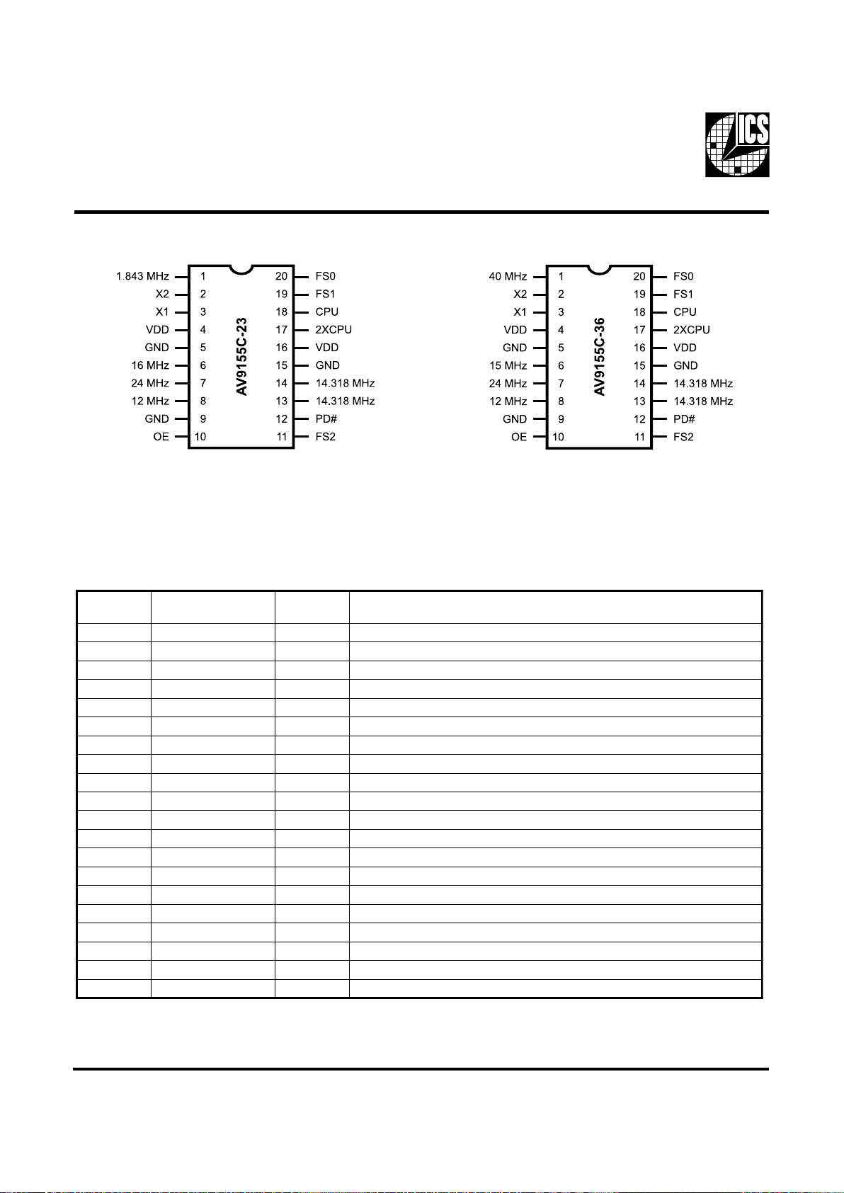
Pin Configuration
Pin Descriptions for A V9155C-23, -36
20-Pin DIP or SOIC
20-Pin DIP or SOIC
NIP
REBMUN
NIP
EMAN
EPYTNOITPIRCSED
1zHM04/348.1tuptuO.tuptuokcolc)63-(ISCSzHM04/)32-(zHM48.1
22XtuptuO.noitcennoclatsyrC
31XtupnI.noitcennoclatsyrC
4DDV- .)V0.5roV3.3(ylppusrewoplatigiD
5DNG-.dnuorglatigiD
6zHM51/zHM61tuptuO.tuptuokcolc)63-(zHM51/)32-(zHM61
7zHM42tuptuO.tuptuokcolcO/Inoitanibmoc/ksidyppolfzHM42
8zHM21tuptuO.tuptuokcolcdraobyekzHM21
9DNGA- .)noisrevlanigiro(dnuorggolanA
01EOtupnI).pu-lluplanretnisaH(.wolnehwstuptuollasetatsirT.elbanetuptuO
112SFtupnI).pu-lluplanretnisah32-(.2#tcelesycneuqerfkcolcUPC
21#DPtupnI).pu-lluplanretnisaH(.wolnehwpihceritneffostuhS.nwod-rewoP
31zHM813.41tuptuO.tuptuokcolcecnereferzHM813.41
41zHM813.41tuptuO.tuptuokcolcecnereferzHM813.41
51DNG-.dnuorglatigiD
61DDV- .)V0.5roV3.3(ylppusrewoplatigiD
71UPCX2tuptuO.tuptuokcolcUPCX2
81UPCtuptuO.tuptuokcolcUPCX1
911SFtupnI).pu-lluplanretnisah32-(.1#tcelesycneuqerfkcolcUPC
020SFtupnI).pu-lluplanretnisah32-(.0#tcelesycneuqerfkcolcUPC
5
AV9155C
CLOCK#2 CPU and 2XCPU
*V
DD
minimum 3.15V
PERIPHERAL CLOCKS
REFERENCE CLOCKS
CLOCK#2 CPU and 2XCPU
*VDD minimum 3.15V
PERIPHERAL CLOCKS
REFERENCE CLOCKS
KLCMMOC
)1niP(
niP(KLCSUB
)6
KLCDF
)7niP(
KLCBK
)8niP(
348.1614221
KLCISCS
)1niP(
niP(KLCSUB
)6
KLCDF
)7niP(
KLCBK
)8niP(
04514221
1KLCFER
)31niP(
2KLCFER
)41niP(
813.41813.41
1KLCFER
)31niP(
2KLCFER
)41niP(
813.41813.41
2SF
)11niP(
1SF
)91niP(
0SF
)02niP(
UPCX2
)71niP(
UPC
)81niP(
0
0
0
0
1
1
1
1
0
0
1
1
0
0
1
1
0
1
0
1
0
1
0
1
8
61
06
04
05
66.66
*08
*001
4
8
03
02
52
33.33
*04
*05
Functionality - A V9155C-23
(Using 14.318 MHz input. All frequencies in MHz.)
Functionality - A V9155C-36
(Using 14.318 MHz input. All frequencies in MHz.)
2SF
)11niP(
1SF
)91niP(
0SF
)02niP(
UPCX2
)71niP(
UPC
)81niP(
0
0
0
0
1
1
1
1
0
0
1
1
0
0
1
1
0
1
0
1
0
1
0
1
*57
23
06
04
05
66.66
*08
25
*5.73
61
03
02
52
33.33
*04
62

6
A V9155C
Electrical Characteristics at 5V
Absolute Maximum Ratings
VDD referenced to GND . . . . . . . . . . . . . . . . . . . . . . 7V
Voltage on I/O pins referenced to GND. . . . . . . . . . . GND -0.5V to VDD +0.5V
Operating temperature under bias. . . . . . . . . . . . . . . . 0°C to +70°C
Power dissipation . . . . . . . . . . . . . . . . . . . . . . . . . . . . 0.5 Watts
Storage temperature . . . . . . . . . . . . . . . . . . . . . . . . . . -40°C to +150°C
Stresses above those listed under Absolute Maximum Ratings may cause permanent damage to the device. This is a stress rating
only and functional operation of the device at these or any other conditions above those indicated in the operational sections
of the specifications is not implied. Exposure to absolute maximum rating conditions for extended periods may affect product
reliability.
V
DD
= 4.0 to 5.5V (5V +10%/-20%); T
A=0
°C to 70°C unless otherwise stated
Notes:
1 Parameter is guaranteed by design and characterization, not subject to production testing.
scitsiretcarahCCD
RETEMARAPLOBMYSSNOITIDNOCTSETNIMPYTXAMSTINU
egatloVwoLtupnIVLIVDDV5=--8.0V
egatloVhgiHtupnIVHIVDDV5=0.2--V
#DP,egatloVhgiHtupnIVDPHIVDDtupni#DProf,V5=2.2--V
tnerruCwoLtupnIILIVNI)nippu-llup(V0=-6153Aµ
tnerruChgiHtupnIIHIVNIV=DD5-05Aµ
egatloVwoLtuptuOVLOILOAm8=-51.04.0V
egatloVhgiHtuptuO
1
VHOIHOAm52-=4.27.3-V
tnerruCwoLtuptuO
1
ILOVLO8.0=5123-Am
tnerruChgiHtuptuO
1
IHOVHOV0.2=-84-03-Am
tnerruCylppuSIDDzHM66,dedaolnU-8306Am
nwod-rewoP,tnerruCylppuSIDPDDKLCSx 0=#DP000=-7.05.1Am
egnahCycneuqerFtuptuO
dnaylppuSrevo
erutarepmeT
1
FD
lacipytottcepserhtiW
ycneuqerf
-200.010.0%
tnerructiucrictrohS
1
ICSkcolctuptuohcaE5204-Am
ecnaticapaCtupnI
1
CI 2X,1XtpecxE--01Fp
ecnaticapaCdaoL
1
CL 2X,1XsniP-02-Fp
rotsiseRpu-lluP
1
RupVtaNIV=DDV1-021053007mhok

7
AV9155C
Electrical Characteristics at 5V
VDD = 4.0 to 5.5V (5V +10%/-20%); T
A=0
°C to 70°C unless otherwise stated
Notes:
1 Parameter is guaranteed by design and characterization, not subject to production testing.
scitsiretcarahCCA
RETEMARAPLOBMYSSNOITIDNOCTSETNIMPYTXAMSTINU
emiTesiRkcolCtupnI
1
trCI--02sn
emiTllaFkcolCtupnI
1
tfCI--02sn
emitesiRtuptuO
1
tr V0.2ot8.0,daolFp52-5.12sn
emitesiR
1
tr
%08ot%02,daolFp52
VDD
-0.20.4sn
emitllaFtuptuO
1
tf V8.0ot0.2,daolFp52-0.10.2sn
emitllaF
1
tf
%02ot%08,daolFp52
VDD
-3.10.3sn
elcycytuD
1
dt V4.1tadaolFp5255/5425/8454/55%
,elcycytuD
1
skcolcecnereferdtV4.1tadaolFp52633405%
amgiseno,rettiJ
1
05ot02,
skcolczHM
1
04dnaUPCno
UPCX2nozHM001ot
t1sljselcyc000,01-8.00.2%
amgiseno,rettiJ
1
dexif,
02wolebskcolc&kcolc
zHM04woleb,UPCnozHM
UPCX2no
t2sljselcyc000,01-8.00.2%
etulosba,rettiJ
1
05ot02,
skcolczHM
1
04dnaUPCno
UPCX2nozHM001ot
t1bajselcyc000,010.4-0.20.4%
etulosba,rettiJ
1
kcolcdexif,
nozHM02wolebskcolc&
nozHM04woleb,UPC
UPCX2
t2bajselcyc000,010.5-0.20.5%
ycneuqerFtupnI
1
fni2813.4123zHM
tuptuOmumixaM
ycneuqerF
1
ftuoUPCX2ta001022zHM
dnaUPCneewtebwekskcolC
stuptuoUPCX2
1
Tks-041004sp
emiTpu-rewoP
1
tOPtzHM66ot-851sm
emiTnoitisnarTycneuqerF
1
ttfHM66.66ot8morf-5.621sm
zHM08ot23morf-8.12.3sm
zHM23ot08morf-5.20.5sm

8
A V9155C
Electrical Characteristics at 3.3V
V
DD
=3.0V to 3.7V, T
A=0
°C to 70°C unless otherwise stated
Notes:
1 Parameter is guaranteed by design and characterization, not subject to production testing.
scitsiretcarahCCD
RETEMARAPLOBMYSSNOITIDNOCTSETNIMPYTXAMSTINU
egatloVwoLtupnIVLIVDDV3.3=--V2.0DDV
egatloVhgiHtupnIVHIVDDV3.3=V7.0DD- - V
#DP,egatloVhgiHtupnIVDPHIVDDtupni#DProf,V3.3=2.2--V
tnerruCwoLtupnIILI)nippu-llup(V0=NIV-1152Aµ
tnerruChgiHtupnIIHIVNIV=DD5-05Aµ
egatloVwoLtuptuOVLOILOAm4=-V50.0DDV1.0DDV
egatloVhgiHtuptuO
1
VHOIHOAm5.3-=-V49.0DD- V
tnerruCwoLtuptuO
1
ILOVLOV2.0=DD2122-Am
tnerruChgiHtuptuO
1
IHOVHOV7.0=DD-11-5.6-Am
tnerruCylppuSIDDzHM6.66,dedaolnU-8254Am
nwod-rewoP,tnerruCylppuSIDPDDKLCSx 0=#DP000=-52.05.0Am
egnahCycneuqerFtuptuO
dnaylppuSrevo
erutarepmeT
1
FD
lacipytottcepserhtiW
ycneuqerf
-200.010.0%
tnerructiucrictrohS
1
ICSkcolctuptuohcaE0203-Am
ecnaticapaCtupnI
1
CI 2X,1XtpecxE--01Fp
ecnaticapaCdaoL
1
CL 2X,1XsniP-02-Fp
rotsiseRpu-lluP
1
RupVtaNIV=DDV1-021033056mhok

9
AV9155C
Electrical Characteristics at 3.3V
VDD = +3.3V±10%, TA=0°C to 70°C unless otherwise stated
Notes:
1 Parameter is guaranteed by design and characterization, not subject to production testing.
2 Output frequencies on 2XCPU of 80 or 100 MHz require minimum V
DD of 3.15V (3.3 -5%).
scitsiretcarahCCA
RETEMARAPLOBMYSSNOITIDNOCTSETNIMPYTXAMSTINU
emiTesiRkcolCtupnI
1
trCI--02sn
emiTllaFkcolCtupnI
1
tfCI--02sn
emitesiR
1
tr
%08ot%02,daolFp52
VDD
-0.30.4sn
emitllaF
1
tf
%02ot%08,daolFp52
VDD
-8.15.2sn
elcycytuD
1
dt V%05tadaolFp52DD048406%
,elcycytuD
1
skcolcecnereferdtV%05tadaolFp52DD336376%
amgiseno,rettiJ
1
t1sljselcyc000,01-8.05.2%
etulosba,rettiJ
1
t1bajselcyc000,010.5-0.20.5%
ycneuqerFtupnI
1
fni2813.4123zhM
ycneuqerFtuptuOmumixaM
2,1
ftuoUPCX2ta7041-zHM
dnaUPCneewtebwekskcolC
stuptuoUPCX2
1
Tks001022005sp
emiTpu-rewoP
1
ttOPzHM66ot-621sm
emiTnoitisnarTycneuqerF
1
ttfzHM0.05ot8morf-621sm

10
A V9155C
A V9155C-01 and AV9155C-02
CLOCK#2 CPU and 2XCPU
PERIPHERAL CLOCKS
Actual Output Frequencies
(Using 14.318 MHz input. All frequencies in MHz.)
AV9155C-23
CPU CLOCK
PERIPHERAL CLOCKS
AV9155C-36
CPU CLOCK
PERIPHERAL CLOCKS
2SF
)11niP(
1SF
)91niP(
0SF
)02niP(
UPCX2
)71niP(
UPC
)81niP(
0
0
0
0
1
1
1
1
0
0
1
1
0
0
1
1
0
1
0
1
0
1
0
1
05.7
15.51
22.23
90.04
11.05
28.66
81.08
32.001
57.3
67.7
11.61
50.02
60.52
14.33
90.04
11.05
2SF
)11niP(
1SF
)91niP(
0SF
)02niP(
UPCX2
)71niP(
UPC
)81niP(
0
0
0
0
1
1
1
1
0
0
1
1
0
0
1
1
0
1
0
1
0
1
0
1
450.8
200.61
578.95
688.93
311.05
674.66
181.08
622.001
720.4
100.8
639.92
349.91
750.52
832.33
190.04
311.05
KLCMMOC
)1niP(
KLCSUB
)7niP(
KLCDF
)6niP(
KLCBK
)8niP(
00.0400.5100.4200.21
2SF
)11niP(
1SF
)91niP(
0SF
)02niP(
UPCX2
)71niP(
UPC
)81niP(
0
0
0
0
1
1
1
1
0
0
1
1
0
0
1
1
0
1
0
1
0
1
0
1
071.57
049.13
631.06
090.04
311.05
674.66
181.08
309.15
*585.73
079.51
860.03
540.02
750.52
832.33
190.04
259.52
KLCMMOC
)1niP(
niP(KLCSUB
)6
KLCDF
)7niP(
KLCBK
)8niP(
648.100.61ro10.2300.4200.21
KLCMMOC
)1niP(
KLCSUB
)6niP(
KLCDF
)7niP(
KLCBK
)8niP(
648.100.6100.4200.21

11
AV9155C
Notes:
1. ICS recommends the use of an isolated ground plane for the AV9155C. All grounds shown on this drawing should be
connected to this ground plane. This ground plane should be connected to the system ground plane at a single point. Please
refer to AV9155C Board Layout Diagram.
2. A single power supply connection for all VDD lines at the 2.2µF decoupling capacitor is recommended to reduce interaction
of analog and digital circuits. The 0.1µF decoupling capacitors should be located as close to each VDD pin as possible.
3. A 33
ΩΩ
ΩΩ
Ω series termination resistor should be used on any clock output which drives more than one load or drives a long trace
(more than about two inches), especially when using high frequencies (>50 MHz). This termination resistor is put in series
with the clock output line close to the clock output. It helps improve jitter performance and reduce EMI by damping standing
waves caused by impedance mismatches in the output clock circuit trace.
4. The ferrite bead does not enhance the performance of the AV9155C, but will reduce EMI radiation from the VDD line.
AV9155C Recommended External Circuit

12
A V9155C
AV9155C Recommended Board Layout
This is the recommended layout for the AV9155C to maximize clock performance. Shown are the power and ground
connections, the ground plane, and the input/output traces.
Use of the isolated ground plane and power connection, as shown, will prevent stray high frequency ground and system noise
from propagating through the device. When compared to using the system ground and power planes, this technique will
minimize output clock jitter. The isolated ground plane should be connected to the system ground plane at one point, near the
2.2µF decoupling cap. For lowest jitter performance, this isolated ground plane should be kept away from clock output pins
and traces. Keeping the isolated ground plane area as small as possible will minimize EMI radiation. Use a sufficient gap
between the isolated ground plane and system ground plane to prevent AC coupling. The ferrite bead in the VDD line optional,
but will help reduce EMI.
The traces to distribute the output clocks should be over a system ground or power supply plane. The trace width should be about
two times the thickness of the PC board between the trace and the underlying plane. These guidelines help minimize clock jitter
and EMI radiation. The traces to distribute power should be as wide as possible.

13
AV9155C
Ordering Information
Example:
20-Pin DIP Packa ge
AV9155C-02CN20,
AV9155C-23CN20, AV9155C-36CN20
Notes:
Tape and reel packaging should be ordered with the suffix T&R. For instance, if the -01 in DIP and tape & reel is required,
order the part as AV9155C-01CN20T&R.
ICS XXXX-PPP M X#W
Lead Count & Package Width
Lead Count=1, 2 or 3 digits
W=.3” SOIC or .6” DIP; None=Standard Width
Package Type
N=DIP (Plastic#) T&R=Tape and Reel
Pattern Number (2 or 3 digit number for parts with ROM code patterns)
Device Type (consists of 3 or 4 digit numbers)
Prefix
ICS, A V=Standard Device

14
A V9155C
Ordering Information
AV9155C-01CW20, AV9155C-02CM20,
A V9155C-23CM20, A V9155C-36CM20
TNUOCDAELL41L61L81L02L42L82L23
LNOISNEMID453.0404.0454.0405.0406.0407.0408.0
ICS XXXX-PPP M X#W
Lead Count & Package Width
Lead Count=1, 2 or 3 digits
W=.3” SOIC or .6” DIP; None=Standard Width
Package Type
W=SOIC T&R=Tape and Reel
Pattern Number (2 or 3 digit number for parts with ROM code patterns)
Device Type (consists of 3 or 4 digit numbers)
Prefix
ICS, AV=Standard Device
Example:
 Loading...