Integrated
Circuit
Systems, Inc.
Preliminary Product Preview
Low Cost 16-Pin Frequency Generator
AV9154A-39
General Description
The ICS9154A-39 is a 0.8mm technology low-cost frequency
generator designed for general purpose PC and disk drive
applications. However, because the ICS9154A-39 uses 0.8mm
technology and the latest phase-locked loop architecture, it
offers significant performance advantages that enable the
device to be used in high performance systems when clock
jitter is a key design issue.
The ICS9154A-39 guarantees a 45/55 duty cycle over all
frequencies. In addition, a worst case jitter of ±250ps is
achieved.
The CPU clock offers the unique feature of smooth, glitchfree transitions from one frequency to the next, making this
the ideal device to use whenever slowing the cpu speed. The
ICS9154A-39 makes a gradual transition between
frequencies.
Features
All loop filter components internal
5V operation
16-pin 150-mil SOIC
Power-down control of CPU clock and Fixed Clock
when PD# goes low
Output enable control of all output pins
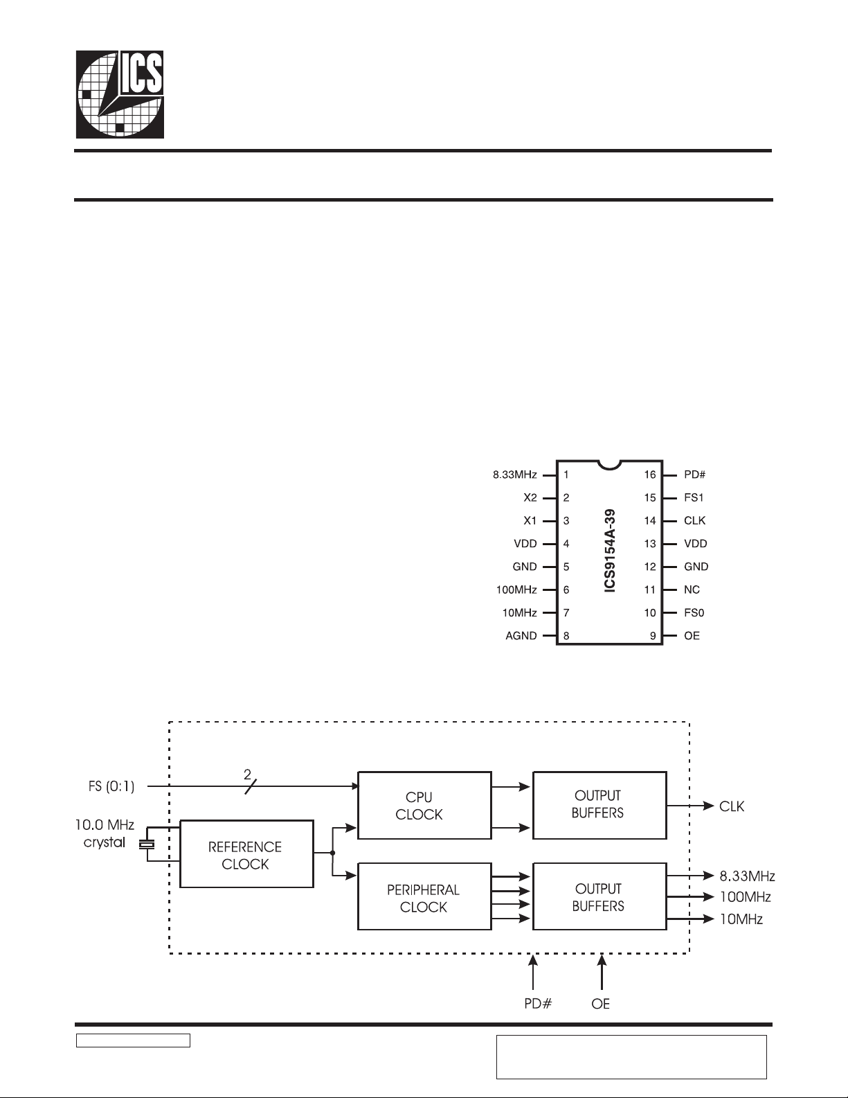
Pin Configuration
Block Diagram
9154-39 Rev B 09/18/97
16-Pin SOIC
PRODUCT PREVIEW documents contain information on new
products in the sampling or preproduction phase of development.
Characteristic data and other specifications are subject to change
without notice.

AV9154A-39
Preliminary Product Preview
Pin Descriptions
PIN
NUMBER
1 8.33 MHz OUT 8.33 MHz output clock.*
2 X2 OUT Crystal Out.
3 X1 IN Crystal In, nominally 10.0 MHz.
4 VDD PWR Digital power (+5V).
5 GND PWR Digital ground.
6 100 MHz OUT 100 MHz clock output.*
7 10 MHz OUT 10 MHz keyboard clock output.*
8 AGND PWR Analog ground.
9 OE IN Tristates outputs when low.
10 FS0 IN Frequency select 0 for CPU clock.
11 NC - No connect (Do not connect to this pin.).
12 GND PWR Digital ground.
13 VDD PWR Digital power (+5V).
14 CPUCLK OUT CPU clock output.
15 FS1 IN Frequency select 1 for CPU clock.
16 PD# IN
PIN NAME TYPE DESCRIPTION
Power-down, shuts off internal clocks and forces outputs to
low logic level when input pulled logic low.
Note: The following input pins are pulled-up to VDD internal: 9, 10, 15 and 16.
Functionality
FS1 FS0 CLK(MHz)
0 0 40.0
0 1 30.0
1 0 37.0
1 1 25.0
These frequencies assume an input frequency of 10.0 Mhz.
2
 Loading...