

Integrated
Circuit
Systems, Inc.
General Description Features
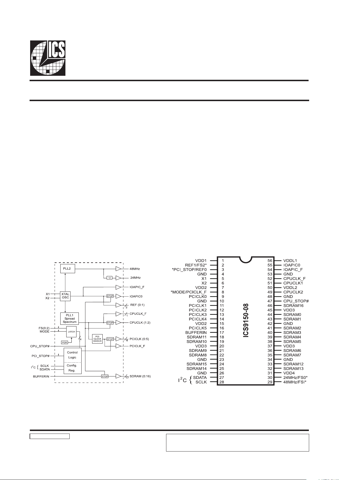
ICS9150-08
Block Diagram
Pentium is a trademark of Intel Corporation
I2C is a trademark of Philips Corporation.
Frequency Generator & Integrated Buffers for Pentium/Pro™
9150-08 Rev E 09/28/98
Pin Configuration
3.3V outputs: SDRAM, PCI, REF, 48/24MHz
2.5V outputs: CPU, IOAPIC
20 ohm CPU clock output impedance
20 ohm PCI clock output impedance
Skew from CPU (earlier) to PCI clock - 1 to 4 ns, center
2.6 ns.
No external load cap for C
L
=18pF crystals
±250 ps CPU, PCI clock skew
250ps (cycle to cycle) CPU jitter
Smooth CPU frequency switching from 50 to 133 MHz
I
2
C interface for programming
2ms power up clock stable time
Clock duty cycle 45-55%.
56 pin 300 mil SSOP package
3.3V operation, 5V tolerant inputs (with series R)
<5.5ns SDRAM propagation delay from Buffer Input
56-Pin SSOP
The ICS9150-08 generates all clocks required for high speed
RISC or CISC microprocessor systems such as Intel
PentiumPro or Cyrix. Eight different reference frequency
multiplying factors are selectable.
Features include three CPU, seven PCI and seventeen SDRAM
clocks. Two reference output is available equal to the crystal
frequency, plus two IOAPIC outputs powered by VDDL1.
One 48 MHz for USB is provided plus a 24 MHz. Spread
Spectrum built in at ±0.5% or ±0.25% modulation to reduce
EMI. Serial programming I
2
C interface allows changing
functions, stop clock programing and Frequency selection. It
is not recommended to use dual function I/O pins to clock
slots (ISA, PIC, CPU, DIMM). The add on card may have a
pull-up or pull-down. Additionally, the device meets the
Pentium power-up stabilization, which requires that CPU and
PCI clocks be stable within 2ms after power-up.
High drive PCICLK and SDRAM outputs typically provide
greater than 1 V/ns slew rate into 30pF loads. CPUCLK outputs
typically provide better than 1V/ns slew rate into 20pF loads
while maintaining 50±5% duty cycle. The REF, 24 and 48 MHz
clock outputs typically provide better than 0.5V/ns slew rates
into 20pF.
Power Groups
VDD1 = REF (0:1), X1, X2
VDD2 = PCICLK_F, PCICLK(0:5)
VDD3 = SDRAM (0:18), supply for PLL core,
VDD4 = 48MHz, 24MHz
VDDL1 = IOAPIC_F
VDDL2 = CPUCLK_F (1:2)
* Internal Pull-up Resistor of 240K to 3.3V on indicated inputs
ICS reserves the right to make changes in the device data identified in this
publication without further notice. ICS advises its customers to obtain the latest
version of all device data to verify that any information being relied upon by the
customer is current and accurate.
2
ICS9150-08
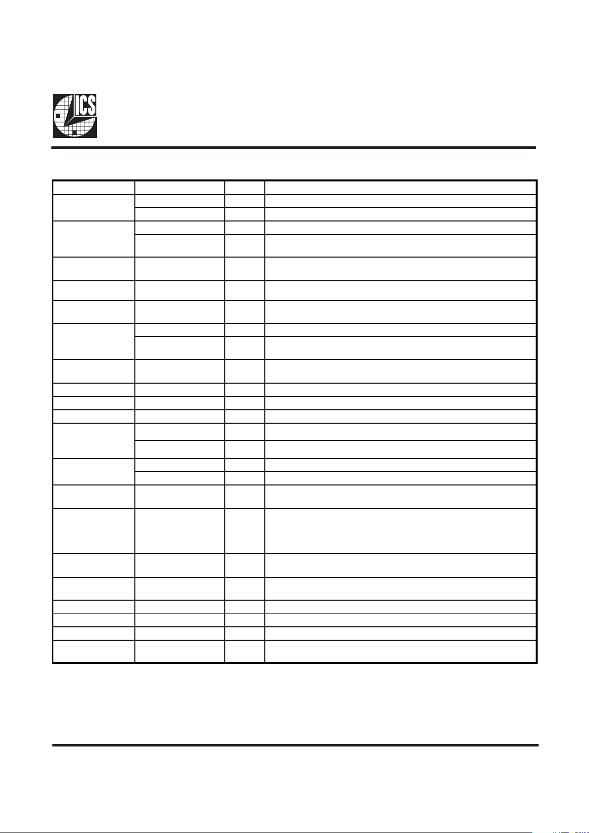
Pin Descriptions
Notes:
1: Bidirectional input/output pins, input logic levels are latched at internal power-on-reset. Use 10Kohm resistor to
program logic Hi to VDD or GND for logic low.
PIN NUMBER PIN NAME TYPE DESCRIPTION
2
REF1 OUT 14.318 MHz reference clock output
FS2
1
IN Latched frequency select input. Has pul l-up to VDD2.
3
REF0 OUT 14. 318MHz reference clock out put
PCI_STOP# IN
Halts PCICLK (0:5) at logic "0" level when low.
(in mobile, MODE=0)
4, 10, 23, 26, 34, 42,
48, 53
GND PW R Ground.
5 X1 IN 14.318MHz input. Has internal load cap, (nominal 33pF).
6 X2 OUT
Crystal output. Has internal l oad cap (33pF) and f eedback
resistor to X1
8
PCICLK_F OUT Free run ning BUS clock not afected by PCI_STOP#
MODE
1
IN
Latched input for MODE select . Converts pin 3 to PCI_STOP# when
low for power management.
9, 11, 12,
13, 14, 16
PCICLK (0:5) OUT PCI Clock Outputs.
17 BUFFERIN IN I nput for Buffers
27 SDATA IN Serial data i n for serial config port. (I
2
C)
28 SCLK IN Clo ck input for s erial config port . (I
2
C)
30
24MHz OUT 24MHz clock output for Super I/O or FD.
FS0
1
IN Latched frequency select input. Has pul l-up to VDD4.
29
48MHz OUT 48MHz clock output for USB.
FS1
1
IN Latched frequency select input. Has pul l-up to VDD2.
1, 7, 15, 20,
31, 37, 45
VDD2, VDD1,
VDD3, VDD4
PWR Nominal 3.3 V power supply, see power groups for function.
18, 19, 21, 22, 24,
25, 32, 33, 35, 36,
38, 39, 40 41, 43,
44, 46
SDRAM
(1:8) (15:12) (7:0), 16
OUT SDRAM clocks
47 C PU_ STOP # IN
Halts CPUCLK (1:2), IOAPIC0, SDRAM (0:16) clocks at logic "0"
level when low.
50, 56 VDDL2, VDDL1 PWR
CPU and IOAPIC clock buffer power supply, either 2.5 or 3.3V
nominal.
55 IOAPIC0 OUT IOAPIC clock output. (14.318 MHz) Poweredby VDDL1
51, 49 CPUCLK (1:2) OUT CPU Output clocks. Powered by VDDL2 (60 or 66. 6MHz)
52 CPUCLK_F OUT Free running CPU output clock. Not affected ty the CPU_STOP#.
54 IOAPIC_F OUT
Freerunning IOAPIC clock output. Not affected by the CPU_STOP#
(14.31818 MHz) Powered by VDDL1
3
ICS9150-08
Functionality
VDD1,2,3 = 3.3V±5%, V
DDL
1,2 = 2.5V±5% or 3.3±5%, TA=0 to 70°C
Crystal (X1, X2) = 14.31818MHz
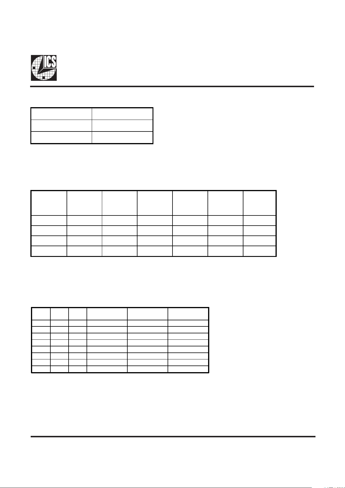
Power Management Functionality
Mode Pin - Power Management Input Control
FS2 FS1 FS0
CPU
(MHz)
PCICLK
(MHz)
REF, IO AP IC
(M Hz)
1 1 1 100.2 33.3 (C PU/3) 14.3 18
1 1 0 133.3
1
33.3 (CPU/4)
1
14.318
101 112
1
37.3
1
14.318
1 0 0 103 34.3 (CPU/3) 14.318
0 1 1 66.8 33.4 (CPU/2) 14.318
0 1 0 83.3 41.65 (CPU/2) 14.318
0 0 1 75 37.5 (CPU/2) 14 .31 8
0 0 0 50 25 (CPU/2) 14.318
CPU_STOP# PCI_STO P#
CPUCLK
Outputs
PCICLK
(0:5)
PCICLK_F ,
REF ,
24/48MHz
and SDRAM
Crystal
OSC
VCO
0 1 Stopped Low Running Running Running Running
1 1 Running Running Running Running Running
1 0 R unning Stopped Low Running Running Runni ng
0 0 Stopped Low Stopp ed Low Running Ru nning Runni ng
MODE, Pin 8
(Latched Input)
Pin 3
0
PCI_STOP#
(INPUT)
1
Ref 0
(OUTPUT)
Note1. Performance not guaranteed
4
ICS9150-08
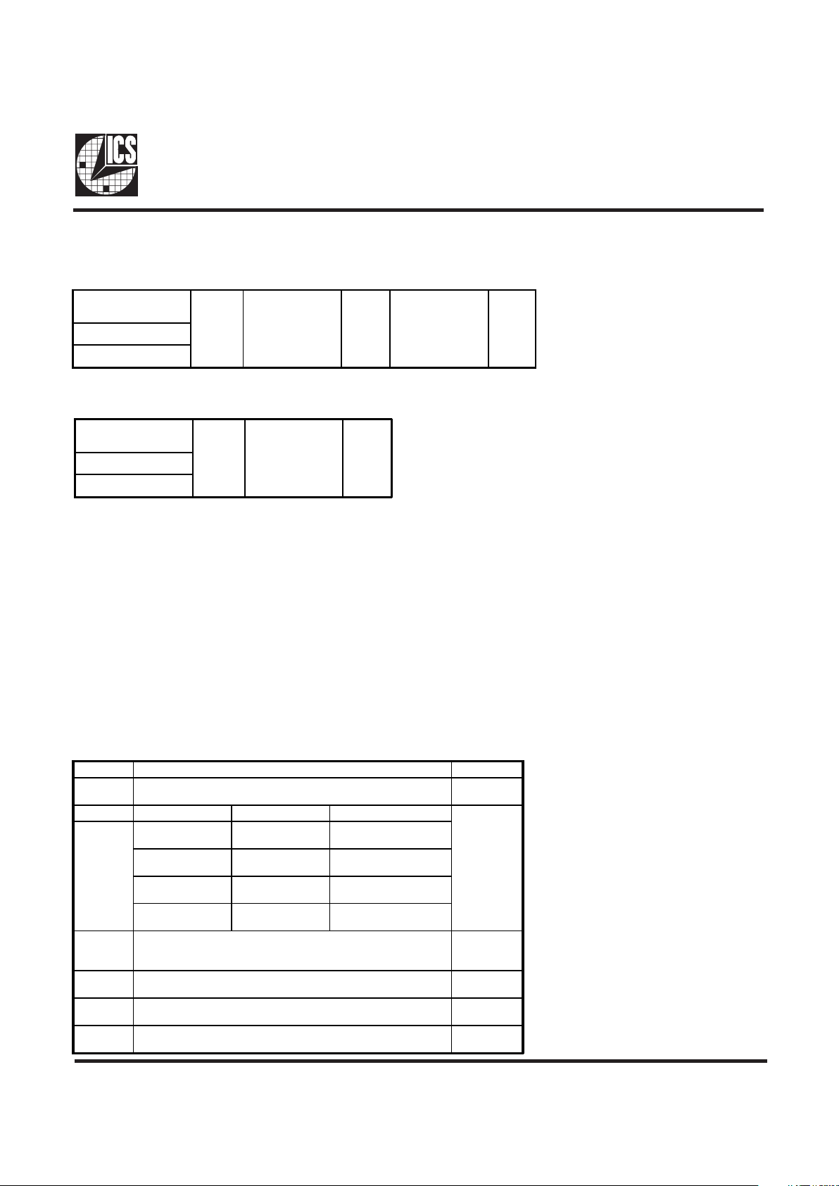
Byte0: Functionality and Frequency Select Register (default = 0)
Serial Configuration Command Bitmap
A. For the clock generator to be addressed by an I2C controller, the following address must be sent as a start sequence,
with an acknoledge bit between each byte.
B. The clock generator is a slave/receiver I
2
C component. It can read back the data stored in the latches for verification. (set
R/W# to 1 above) Read-Back will support Intel PIIX4 "Block-Read" protocol, with a "Byte count" following the
address with R/W#=1, then proceding to Byte 0, 1, 2, ...until STOP.
C. The data transfer rate supported by this clock generator is 100K bits/sec (standard mode)
D. The input is operating at 3.3V logic levels.
E. The data byte format is 8 bit bytes.
F. To simplify the clock generator I
2
C interface, the protocol is set to use only "Block-Writes" from the controller. The
bytes must be accessed in sequential order from lowest to highest byte with the ability to stop after any complete byte
has been transferred. The Command code and Byte count shown above must be sent, but the data is ignored for those
two bytes. The data is loaded until a Stop sequence is issued.
G.. At power-on, all registers are set to a default condition. Byte 0 defaults to a 0, Bytes 1 through 5 default to a 1 (Enabled
output state).
General I2C serial interface information
I2C is a trademark of Philips Corporation
Then Byte 0, 1, 2, etc in
sequence until STOP.
Clock Generator
Address (7 bits)
ACK
+ 8 bits dummy
command code
ACK
+ 8 bits dummy
Byte count
ACK
A(6:0) & R/W#
D2
(H)
Then Byte 0, 1, 2, etc. in
sequence until STOP.
Clock Generat or
Address (7 bits)
ACK
Byte Count
Readback
ACK
A(6:0) & R/W#
D3
(H)
Bit Description PWD
Bit 7
0 - ±0.25% Spread S pectrum Mod ulation
1 - ±0.5% Spread S pectrum Mo dulation
0
Bit6 Bit5 Bit4 CPU clock PCI
Note1
Bit 6:4
111
110
100.2
133.3
2
33.3 (CPU /3)
33.3 (CPU/4)
2
101
100
112.0
2
103
37.3 (CPU/3)
2
34.3 (CPU /3)
011
010
66.8
83.3
33.4 (CPU /2)
41.65(CPU/2)
001
000
75
50
37.5 (CPU /2)
25 (CPU/2)
Bit 3
0 - Frequency is selected by hardware select, Latched
Inputs
1 - Frequency is selected by Bit 6:4 (above)
0
Bit 2
0 - Spread Spectrum center spread type.
1 - Spread Spectrum down spread type.
0
Bit 1
0 - Normal
1 - Spread Spectrum Enabled
0
Bit 0
0 - Running
1- Tristate all outputs
0
Note1. Default at Power-up will be for
latched logic inputs to define
frequency. Bits 4, 5, 6 are default
to 000, and if bit 3 is written to a 1
to use Bits 6:4, then these should
be defined to desired frequency at
same write cycle.
Note2. Performance not guaranteed
Note: PWD = Power-Up Default

5
ICS9150-08
Byte 1: CPU, Active/Inactive Register
(1= enable, 0 = disable)
BIT PI N# PWD DESCRIPTIO N
Bit 7 - 1 Reserved
Bit 6 - 1 Reserved
Bit 5 - 1 Reserved
Bit 4 - 1 Reserved
Bit 3 46 1 SDRAM16 (Act/Inact)
Bit 2 49 1 CPUCLK2 (Act/Inact)
Bit 1 51 1 CPUCLK1 (Act/Inact)
Bit 0 52 1 CPUCLK0 (Act/Inact)
Byte 2: PCI, Active/Inactive Register
(1= enable, 0 = disable)
BIT PIN# PWD DESCRIPTION
Bit 7 - 1 Reserved
Bit 6 8 1 PCICLKF (Act/Inact)
Bit 5 16 1 PCICLK5 (Act/Inact)
Bit 4 14 1 PCICLK4 (Act/Inact)
Bit 3 13 1 PCICLK3 (Act/Inact)
Bit 2 12 1 PCICLK2 (Act/Inact)
Bit 1 11 1 PCICLK1 (Act/Inact)
Bit 0 9 1 PCICLK0 (Act/Inact)
Notes:
1. Inactive means outputs are held LOW and are disabled
from switching.
2. Latched Frequency Selects (FS#) will be inferted logic
load of the input frequency select pin conditions.
BIT PIN# PWD DESCRIPTION
Bit 7 - - Latched FS0#
Bit 6 - 1 Reserved
Bit 5 - 1 Reserved
Bit 4 - - Latched FS1#
Bit 3 - 1 Reserved
Bit 2 - 1 Reserved
Bit 1 - 1 Reserved
Bit 0 - 1 Reserved
Byte 4: Reserved , Active/Inactive Register
(1= enable, 0 = disable)
BIT PIN# PWD DESCRIPTION
Bit 7 - 1 Reserved
Bit 6 - - Latched FS2#
Bit 5 54 1 IOAPIC1 (Act/Inact)
Bit 4 55 1 IOAPIC0 (Act/Inact)
Bit 3 - 1 Reserved
Bit 2 - 1 Reserved
Bit 1 2 1 REF1 (Act/In act)
Bit 0 3 1 REF0 (Act/In act)
Byte 5: Peripheral , Active/Inactive Register
(1= enable, 0 = disable)
Byte 3: SDRAM, Active/Inactive Register
(1= enable, 0 = disable)
BIT PIN# PWD DESCRIPTION
Bit 7 - 1 Reserved
Bit 6 - 1 Reserved
Bit 5 30 1 48MHz (Act/Inact)
Bit 4 29 1 24MHz (Act/Inact)
Bit 3
33, 32,
25, 24
1 SDRAM(12:15) (Act/Inact)
Bit 2
22, 21,
19, 18
1 SDRAM (8:11) (Act/Inact)
Bit 1
39, 38,
36, 35
1 SDRAM (4:7) (Act/Inact)
Bit 0
44, 43,
41, 40
1 SDRAM0 (0:3) (Act/Inact)

6
ICS9150-08
CPU_STOP# Timing Diagram
CPUSTOP# is an asychronous input to the clock synthesizer. It is used to turn off the CPUCLKs for low power operation.
CPU_STOP# is synchronized by the ICS9150-08. All other clocks will continue to run while the CPUCLKs are disabled. The
CPUCLKs will always be stopped in a low state and start in such a manner that guarantees the high pulse width is a full pulse.
CPUCLK on latency is less than 4 CPUCLKs and CPUCLK off latency is less than 4 CPUCLKs.
Notes:
1. All timing is referenced to the internal CPUCLK.
2. CPU_STOP# is an asynchronous input and metastable conditions may exist. This signal is synchronized to the
CPUCLKs inside the ICS9150-08.
3. All other clocks continue to run undisturbed.
4. PCI_STOP# is shown in a high (true) state.
Notes:
1. All timing is referenced to the Internal CPUCLK (defined as inside the device.)
2. PCI_STOP# is an asynchronous input, and metastable conditions may exist. This signal is required to be synchronized
inside the device.
3. All other clocks continue to run undisturbed.
4. CPU_STOP# is shown in a high (true) state.
PCI_STOP# Timing Diagram
PCI_STOP# is an asynchronous input to the ICS9150-08. It is used to turn off the PCICLK (0:5) clocks for low power operation.
PCI_STOP# is synchronized by the ICS9150-08 internally. PCICLK (0:5) clocks are stopped in a low state and started with a full
high pulse width guaranteed. PCICLK (0:5) clock on latency cycles are only one rising PCICLK clock off latency is one PCICLK
clock.
CPUCLK
(Internal)
PCICLK
(Internal)
PCICLK
(Free-running)
CPU_STOP#
PCICLK (0:5)
(External)
PCI_STOP#

7
ICS9150-08
Pins 8, 29, 30, 54 on the ICS9150-08 serve as dual signal
functions to the device. During initial power-up, they act as
input pins. The logic level (voltage) that is present on these
pins at this time is read and stored into a 4-bit internal data
latch. At the end of Power-On reset, (see AC characteristics
for timing values), the device changes the mode of operations
for these pins to an output function. In this mode the pins
produce the specified buffered clocks to external loads.
To program (load) the internal configuration register for these
pins, a resistor is connected to either the VDD (logic 1)
power supply or the GND (logic 0) voltage potential. A 10
Kilohm(10K) resistor is used to provide both the solid CMOS
programming voltage needed during the power-up
programming period and to provide an insignificant load on
the output clock during the subsequent operating period.
Figs. 1 and 2 show the recommended means of implementing
this function. In Fig. 1 either one of the resistors is loaded
onto the board (selective stuffing) to configure the devices
internal logic. Figs. 2a and b provide a single resistor loading
option where either solder spot tabs or a physical jumper
header may be used.
Shared Pin Operation Input/Output Pins
Fig. 1
These figures illustrate the optimal PCB physical layout
options. These configuration resistors are of such a large
ohmic value that they do not effect the low impedance clock
signals. The layouts have been optimized to provide as little
impedance transition to the clock signal as possible, as it
passes through the programming resistor pad(s).

8
ICS9150-08
Fig. 2a
Fig. 2b

9
ICS9150-08
Absolute Maximum Ratings
Supply Voltage . . . . . . . . . . . . . . . . . . . . . . . . . . . . 7.0 V
Logic Inputs . . . . . . . . . . . . . . . . . . . . . . . . . . . . . . GND 0.5 V to V
DD
+0.5 V
Ambient Operating Temperature . . . . . . . . . . . . . 0°C to +70°C
Case Temperature. . . . . . . . . . . . . . . . . . . . . . . . . . 115°C
Storage Temperature . . . . . . . . . . . . . . . . . . . . . . . 65°C to +150°C
Stresses above those listed under Absolute Maximum Ratings may cause permanent damage to the device. These ratings are
stress specifications only and functional operation of the device at these or any other conditions above those listed in the
operational sections of the specifications is not implied. Exposure to absolute maximum rating conditions for extended periods
may affect product reliability.
Electri cal C haracter istics - Input/ Supply/Comm on O utput Par am eters
TA = 0 - 70C; Supp ly Voltage VDD = 3.3 V +/-5% (unless otherwise s t a ted)
PARAMETER SYMBOL COND ITI ON S MIN TYP MAX U NI TS
Input High Voltage V
IH
2V
DD
+0.3 V
Input L ow Volta ge V
IL
VSS-0.3 0.8 V
Suppl y C urrent I
DD
100 180 mA
I
DDL
6.030mA
Input frequenc y F
i
VDD = 3 .3 V; 14.318 MHz
C
IN
Logic Inputs 5 pF
C
INX
X 1 & X2 pins 27 36 45 ps
Transition Time
1
T
trans
To 1st cros sing of target Freq. 1.5 3 ms
Clk Stabiliza tion
1
T
STAB
From VDD = 3.3 V to 1% ta rget Freq. 3 ms
Skew
1
T
CPU-BUSVT
= 1.5 V;
1.0 2.6 4.0 ns
1
G ua renteed by d e sign, not 100% t e sted in pr odu c ti on.
C
L
= 0 pF; Sele c t @ 66M
Inpu t C a pacitance
1

10
ICS9150-08
Elect r i cal C har act er ist i cs - C PU
TA = 0 - 70C; VDD = 3.3 V + / -5%; V
DDL
= 2.5 V +/-5%; CL = 20 pF (unles s otherwise state d)
PARA METER SYMBOL COND ITIO NS MIN TYP MAX UNI TS
O utput Impeda nc e R
DSP2A
1
VO = VDD*(0.5) 10 20
Ω
O utput Impeda nc e R
DSN2A
1
VO = VDD*(0.5) 10 20
Ω
Output High Voltage V
OH2B
IOH = -12.0 mA 2 2.3 V
Output Low Voltage V
OL2B
IOL = 12 mA 0.2 0.4 V
O utput High Curr e nt I
OH2B
VOH = 1 . 7 V -30 -19 m A
O utput L o w Current I
OL2B
VOL = 0. 7 V 25 37 mA
Rise Time t
r2A
1
VOL = 0. 4 V, VOH = 2 . 0 V @ 66M Hz 1.3 1.6 ns
Fa ll T ime t
f2A
1
VOH = 2.0 V, VOL = 0 . 4 V @ 66M Hz 1.1 1.6 ns
Duty Cycle d
t2A
1
VT = 1.25 V 45.0 51.0 55.0 %
Skew
(Window)
t
sk2A
1
VT = 1.25 V 40 250 ps
per iod( norm) V
T
= 1.25 V; 100M Hz 9.75 10 10.2 5 ns
per iod(spr) V
T
= 1.25 V; 100M Hz 9.75 10 10.3 5 ns
Jitter t
j1s2A
1
VT = 1.25 V 120 350 ps
t
j
abs2A
1
VT = 1.25 V -2 50 100 +250 ps
Dev run avg
V
T
= 1.25 V
150 250 ps
1
G ua renteed by des ign, not 100% tes te d in production.
Electr i cal Char act er i sti cs - PC I
TA = 0 - 70C; VDD = 3.3 V +/-5%; CL = 30 pF (unless othe rwise s ta ted)
PA RA METE R SYMBO L CONDITIO N S MI N TYP MAX UN I TS
O utput I mpedance R
DSP1
1
VO = VDD*(0.5 ) 12 23 55
Ω
O utput I mpedance R
DSN1
1
VO = VDD*(0.5 ) 12 20 55
Ω
Output High Voltage V
OH1IOH
= -28 mA 2.4 2.9 V
Output Low Voltage V
OL1IOL
= 23 mA 0.2 0.4 V
Output High Curr ent I
OH1
VOH = 2. 0 V -58 - 22 mA
O utp ut Low Cu rrent I
OL1
VOL = 0.8 V 25 52 mA
Rise Tim e t
r1
1
VOL = 0.8 V, VOH = 2. 4 V 1.5 2.0 ns
Fall Time t
f1
1
VOH = 2. 4 V, VOL = 0. 8 V 1.4 2.0 ns
Duty Cycle d
t1
1
VT = 1.5 V 45.0 50.0 55.0 %
Skew t
sk1
1
VT = 1.5 V 80 250 ps
Jitter t
j1s1
1
VT = 1.5 V 50 150 ps
t
jabs1
1
VT = 1.5 V
200 500 ps
1
Gua renteed by design, not 100% tested in production.

11
ICS9150-08
Elect r i cal Characteri sti cs - SD RA M
TA = 0 - 70C; VDD =V
DDL
3.3 V +/-5%; CL = 30 pF (unles s otherwise sta te d)
PARAMETER SYMBOL CO ND ITIO NS MIN TYP MAX UNI TS
O utput Impeda nc e
R
DSP2A
1
VO = VDD*(0.5) 10 20
Ω
O utput Impeda nc e
R
DSN2 A
1
VO = VDD*(0.5) 10 20
Ω
O utput High V olta ge V
OH2A
IOH = -28 mA 2.4 3 V
O utput Low Voltage V
OL2A
IOL = 19 mA 0.3 0.4 V
Output High Current I
OH2A
VOH = 2. 0 V -72 -42 mA
Output Low Current I
OL2A
VOL = 0.8 V 33 55 mA
Rise Time
t
r2A
1
VOL = 0.8 V, VOH = 2.4 V 1.6 2.0 ns
Fall Time
t
f2A
1
VOH = 2. 4 V, VOL = 0.8 V 1.2 2.0 ns
Duty Cycle
d
t2A
1
VT = 1. 5 V 41 46 51 %
Ske w ( output to o utput )
t
sk2A
1
VT = 1. 5 V 200 600 ps
Ske w Propagation D el ay
( B ufferin to output )
t
sk2A
1
VT = 1.5 V 4.5 55 ns
1
Guarenteed by design, not 100% tested in production.
Electrical Charact eristi c s - 24 M, 48M, REF 1
TA = 0 - 70C; VDD = V
DDL
= 3.3 V +/-5%; CL = 20 p F (unless otherwise sta t ed)
PARAMETER SYMBOL COND ITI ON S MIN TYP MAX UNITS
O utp ut Impedan c e R
DSP5
1
VO = VDD*(0.5) 20 60 W
O utp ut Impedan c e R
DSN5
1
VO = VDD*(0.5) 55 100 W
O utput High Voltage V
OH5
IOH = -8 mA 2.4 2.9 V
Output Low Voltage V
OL5
IOL = 8 mA 0.18 0.4 V
Ou tput High Current I
OH5
VOH = 2.0 V -42 -14 mA
Output Low Current I
OL5
VOL = 0.8 V 16 26 mA
Rise Time t
r5
1
VOL = 0.8 V, VOH = 2.4 V 1.2 2.0 ns
Fall Time t
f5
1
VOH = 2.4 V , VOL = 0.8 V 2.0 2.4 ns
Duty Cycle d
t5
1
VT = 1.5 V 40.0 54.0 60.0 %
Jitter t
j1s5
1
VT = 1.5 V 100 2.1 ns
t
jabs5
1
VT = 1.5 V
0.35 3.5 ns
1
G ua renteed by d e sign, not 100% t e sted in produ c t ion .

12
ICS9150-08
Electrical Characteristics - IOAPIC
TA = 0 - 70C; VDD = V
DDL
= 3.3 V +/-5%; CL = 20 p F (unless otherwise sta t ed)
PARAMETER SYMBOL COND ITI ON S MIN TYP MAX UNITS
O utp ut Impedan c e R
DSP5
1
VO = VDD*(0.5) 20 60 W
O utp ut Impedan c e R
DSN5
1
VO = VDD*(0.5) 55 100 W
O utput High Voltage V
OH5
IOH = -8 mA 2.4 2.9 V
Output Low Voltage V
OL5
IOL = 1.2 mA 0.2 0.4 V
Ou tput High Current I
OH5
VOH = 2.0 V -42 -14 mA
Output Low Current I
OL5
VOL = 0.8 V 10 27 m A
Rise Time t
r5
1
VOL = 0.8 V, VOH = 2.4 V 2.0 2.6 ns
Fall Time t
f5
1
VOH = 2.4 V , VOL = 0.8 V 2.8 3.2 ns
Duty Cycle d
t5
1
VT = 1.5 V 48.0 54.0 58.0 %
Jitter t
j1s5
1
VT = 1.5 V 100 250 ns
t
jabs5
1
VT = 1.5 V
550 800 ps
1
G ua renteed by d e sign, not 100% t e sted in produ c t ion .

13
ICS9150-08
SSOP Package
Ordering Information
ICS9150F-08
Pattern Number (2 or 3 digit number for parts with ROM code patterns)
Package Type
F=SSOP
Device Type (consists of 3 or 4 digit numbers)
Prefix
ICS, AV = Standard Device
Example:
ICS XXXX F - PPP
SYMBOL COMMON DIMENSIO NS VARIATIONS D N
MIN. NOM. MAX. MIN. NOM. MAX.
A .095 .101 .110 AC .620 .625 .630 48
A1 .008 .012 .016 AD .720 .725 .730 56
A2 .088 .090 .092
B .008 .010 .0135
C.005- .010
D See Variations
E .292 .2 96 .299
e0.025 BSC
H .400 .406 .410
h .010 .013 .016
L .024 .032 .040
N See Variations
∝
0° 5° 8°
X .085 .093 .100
ICS reserves the right to make changes in the device data identified in this
publication without further notice. ICS advises its customers to obtain the latest
version of all device data to verify that any information being relied upon by the
customer is current and accurate.
 Loading...