

Integrated
Circuit
Systems, Inc.
General Description Features
ICS9150-04
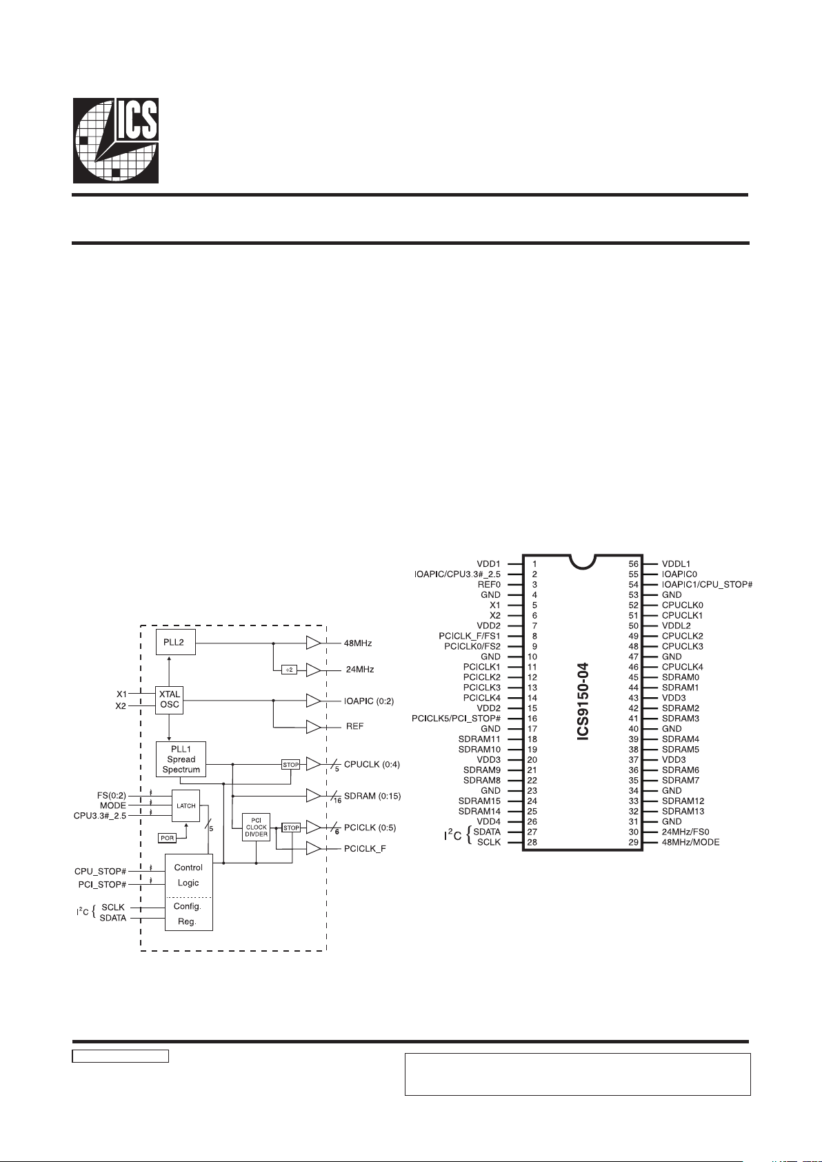
Block Diagram
Pentium is a trademark of Intel Corporation
I2C is a trademark of Philips Corporation.
Pentium Pro™ and SDRAM Frequency Generator
9150-04 RevD 07/27/98
Pin Configuration
Generates five processor, six bus, one 14.31818MHz
(3.3V) three IOAPIC, 16 SDRAM clocks, 48MHz USB
clock and 24MHz Super I/O clock.
Synchronous clocks skew matched to 250 ps window
on CPUCLKs and 500ps window on PCICLKs
Skew from CPU (earlier) to PCI clock - 1 to 4ns, 2.6ns
nom.
Power Management Control Input pins when MODE
Low
VDD(1:4) - 3.3V ±10%
(inputs 5V tolerant w/series R )
VDDL(1:2) - 2.5V or 3.3V ±5%
I
2
C interface for programming stopclocks plus spread
spectrum options (±0.5% or ±1.5%, center spread or
down spread)
56-pin SSOP package
56-Pin SSOP
The ICS9150-04 generates all clocks required for high speed
RISC or CISC microprocessor systems such as Intel
PentiumPro or Cyrix. Eight different reference frequency
multiplying factors are selectable from 50 to 83.3MHz.
Features include five CPU, seven PCI and Sixteen SDRAM
clocks. One reference output is available equal to the crystal
frequency, plus three IOAPIC outputs powered by VDDL1.
One 48 MHz for USB is provided plus a 24 MHz. Spread
Spectrum built in up to ±1.5% modulation to reduce EMI.
Serial programming I
2
C interface allows changing functions,
stop clock programing and Frequency selection. Rise time
adjustment for VDD at 3.3V or 2.5V CPU. Additionally, the
device meets the Pentium power-up stabilization, which
requires that CPU and PCI clocks be stable within 2ms after
power-up.
High drive PCICLK and SDRAM outputs typically provide
greater than 1 V/ns slew rate into 30pF loads. CPUCLK outputs
typically provide better than 1V/ns slew rate into 20pF loads
while maintaining 50±5% duty cycle. The REF 24 and 48 MHz
and SDRAM 12, 13 clock outputs typically provide better
than 0.5V/ns slew rates.
Power Groups
VDD1 = REF, X1, X2
VDD2 = PCICLK_F, PCICLK(0:5)
VDD3 = SDRAM (0:15), supply for PLL core,
VDD4 = 48MHz, 24MHz
VDDL1 = IOAPIC (0:2)
VDDL2 = CPUCLK (0:4)
ICS reserves the right to make changes in the device data identified in this
publication without further notice. ICS advises its customers to obtain the latest
version of all device data to verify that any information being relied upon by the
customer is current and accurate.
2
ICS9150-04
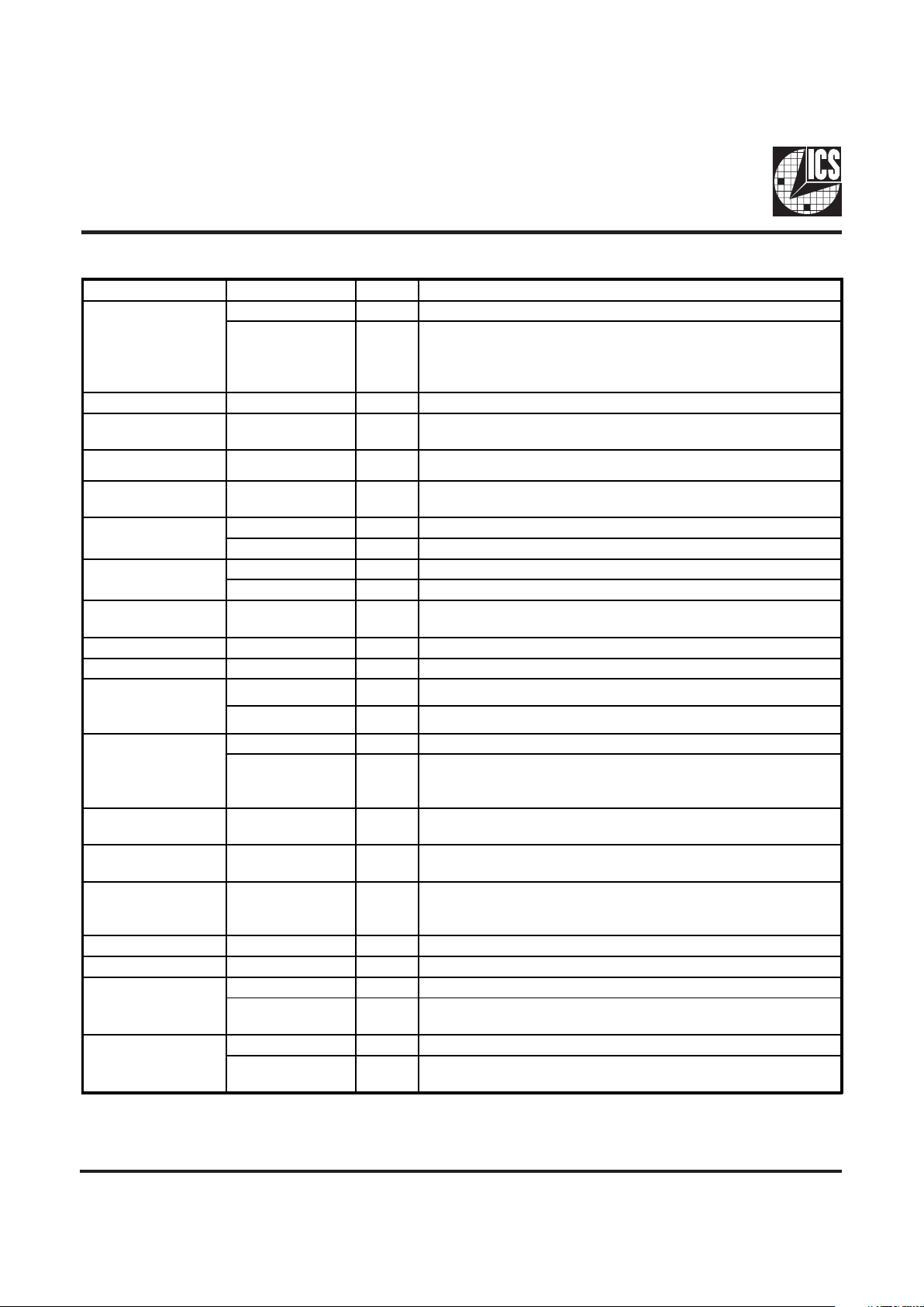
Pin Descriptions
PIN NUMBER PIN NAME TYPE DESCRIPTION
2
IOAPIC2 OUT IOAPIC clock output (14.318MHz) powered by VDDL1
CPU3.3#_2.5 IN
Indic at es whe the r VDDL1 & VDDL2 a re 3.3 o r 2. 5V. Outp ut
buffer strength compensates for VDDL selection to maintain
CPU to SDRAM skew. High = 2.5V, Low = 3.3V. Has pull-up
to VDDL1, mus t us e ser ie s re sis tor for 3. 3 or 5V log ic l evels .
3 REF0 OUT 14.318 MHz reference clock outputs.
4, 10, 17, 23, 31, 34,
40, 47, 53
GND PWR Ground.
5 X1 IN 14.318MHz input. Has internal load cap, (nominal 33pF).
6X2 OUT
Crystal output. Has internal load cap (33pF) and feedback
resistor to X1
8
PCICLK_F OUT Free running BUS clock during PCI_STOP#=0.
FS1
1
IN Latched frequency select input. Has pull-up to VDD2.
9
PCICLK0 OUT BUS clock output
FS2
1
IN Latched frequency select input. Has pull-up to VDD2.
11, 12,
13, 14
PCICLK (1:4) OUT BUS clock outputs.
27 SDATA IN Serial data in for serial config port. (I
2
C)
28 SCLK IN Clock i nput for seri al config port. (I
2
C)
30
24MHz OUT 24MHz clock output for Super I/O or FD.
FS0
1
IN Latched frequency select input. Has pull-up to VDD4.
29
48MHz OUT 48MHz clock output for USB.
MODE
1
IN
Latched input for MODE select. Converts 2 outputs to power
management CPU_STOP# and PCI_STOP# when low. Has pullup to VDD4.
1, 7, 15, 20, 26, 37,43VDD2, VDD1,
VDD3, VDD4
PWR Nominal 3.3V power supply, see power groups for function.
50, 56 VDDL2, VDDL1 PWR
CPU and IOAPIC clock buffer power supply, either 2.5 or 3.3V
nominal.
18, 19, 21, 22, 24,
25, 32, 33, 35 , 36,
38, 39, 41, 42, 44, 45
SDRAM (0:15) OUT SDRAM clocks
55 IOAPIC0 O UT IOAPIC clock output. (14.318 MHz) Poweredby VDDL1
46, 48, 49, 51, 52 CPUCLK (0:4) O UT CPU Output clocks. Powered by VDDL2 (60 or 66.6MHz)
54
IOAPIC1 OUT IOAPIC clock output. (14.31818 MHz) Powered by VDDL1
CPU_STOP# I N
Halts CPUCLK clocks at logic "0" level when low. (in mobile,
MODE=0)
16
PCICL K5 OUT PCI BUS cl ock 5
PCI_STOP# IN
Halts PCICLK (0:4) at logic "0" level when low. (in mobile,
MODE=0)
Notes:
1: Bidirectional input/output pins, input logic levels are latched at internal power-on-reset. Use 10Kohm resistor
to program logic Hi to VDD or GND for logic low.
3
ICS9150-04
Definitions
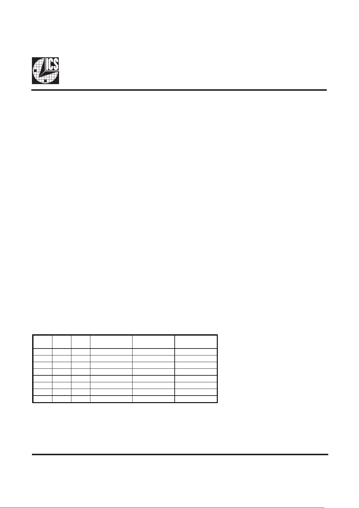
5 Latched Inputs at Internal Power-On Reset:
MODE................................ 48MHz/MODE
CPU 3.3_2.5#V .................. IOAPIC2/CPU3.3#_2.5
FS0 ..................................... 24MHz/FS0
FS1 ..................................... PCICLK_F/FS1
FS2 ..................................... PCICLK0/FS2
Pin shared as
2 Realtime Inputs
Pins 27, 28 - I2C Serial input SDATA & SCLK
Pull-ups
2 pins with input latch or I/O have IOAPIC output function with VDDL1 which can be at 2.5V or 3.3V. These inputs will
have to use series resistor (above 100Ω) to external VIN to be 3.3 & 5V logic input tolerant.
PMOS output stage provides input clamp diode to VDDL.
Nwell resistor Pull-ups 100 to 150KΩ to local VDD
(ie on IOAPIC pins use VDDL1, on FS1, 2 use VDD2, FS0=VDD4 and PCI_STOP#)
Functionality
VDD1,2,3 = 3.3V±5%, V
DDL
1,2 = 2.5V±5% or 3.3±5%, TA=0 to 70°C
Crystal (X1, X2) = 14.31818MHz
FS2 FS1 FS0
CPU,
SDRAM(MHz)
PCICLK (MHz)
REF, IOAPI C
(MHz)
1 1 1 66.8 33.4 (1/2 CPU) 14.318
1 1 0 60.0 30.0 (1/2 CPU) 14.318
1 0 1 75.0 37.5 (1/2 CPU) 14.318
1 0 0 83.3 33.3 14.318
0 1 1 6 8 .5 34.25 (1/2 CPU) 1 4 .3 1 8
0 1 0 8 3 .3 41.65 (1/2 CPU) 1 4 .3 1 8
0 0 1 75.0 32 14.318
0 0 0 50.0 25.0 (1/2 CPU) 14.318
4
ICS9150-04
Mode Pin - Power Management Input Control
Power Management Functionality
Spread Spectrum Functionality
CPU 3.3#_2.5V Buffer selector for CPUCLK driver.
CPU3.3#_2.5
Lat ched I nput Lev el
Buffer Selected
for Operation at:
1 2.5V VD D
0 3 .3V VD D
B YTE0, B it 1
SS_EN
B YTE0, B it 2
SS_TYPE
BYTE0, Bit7
CPU, SDR AM
and PCI CLOCKS
REF, IOAPIC 24,48 M Hz
1
0
0
Frequency modulated in center spread
spectrum mode +1.5%, -1.5%
14.318MHz 24,48MHz
1
Frequency modulated in center spread
spectrum mode +0.5%, -0.5%
14.318MHz 24,48MHz
1
0
F req uenc y mod ula t e d in d ow n s p r e a d
spectrum mode +0%, -3.0%
14.318MHz 24,48MHz
1
F req uenc y mod ula t e d in d ow n s p r e a d
spectrum mode +0%, -1.0%
14.318MHz 24,48MHz
0 X X Normal, Steady frequency mode 14.318MHz 24,48MHz
MODE, Pin 55 Pin 54 Pin 16
0
CPU_STOP#
Input
PCI_STOP#
Input
1
IOAPIC1
Output
PCICLK5
Output
CPU_STOP# PCI_STOP#
CPUCLK
Outputs
PCICLK(0:5)
Outputs
PCICLK_F,
REF, IOAPIC
48MHz
and SDRAM
Crystal
OSC
VCO
0 0 Stopped Low Stopped Low Running Running Running
0 1 Stopped L ow Running Running Running Run ning
1 0 Running Stopped Low Running Running Running
1 1 Runni ng Running Runnin g Running R unning

5
ICS9150-04
VDD(1,2,3,4)
This is the power supply to the internal core logic of the
device as well as the clock output buffers for REF, PCICLK,
and SDRAM.
This pin operates at 3.3V volts. Clocks from the listed buffers
that it supplies will have a voltage swing from Ground to this
level. For the actual guaranteed high and low voltage levels
for the Clocks, please consult the DC parameter table in this
data sheet.
VDDL1,2
This is the power supply for the CPUCLK and IOAPIC output
buffers. The voltage level for these outputs may be 2.5 or
3.3volts. Clocks from the buffers that each supplies will have
a voltage swing from Ground to this level. For the actual
Guaranteed high and low voltage levels of these Clocks,
please consult the DC parameter table in this Data Sheet.
GND
This is the power supply ground (common or negative) return
pin for the internal core logic and all the output buffers.
X1
This input pin serves one of two functions. When the device
is used with a Crystal, X1 acts as the input pin for the
reference signal that comes from the discrete crystal. When
the device is driven by an external clock signal, X1 is the
device input pin for that reference clock. This pin also
implements an internal Crystal loading capacitor that is
connected to ground. With nominal value of 33pF no external
load cap is needed for a CL=17 to 18pF crystal.
X2
This Output pin is used only when the device uses a Crystal
as the reference frequency source. In this mode of operation,
X2 is an output signal that drives (or excites) the discrete
Crystal. The X2 pin will also implement an internal Crystal
loading capacitor that is nominally 33pF.
CPUCLK (0:4)
These Output pins are the Clock Outputs that drive processor
and other CPU related circuitry that requires clocks which are
in tight skew tolerance with the CPU clock. The voltage
swing of these Clocks is controlled by the Voltage level
applied to the VDDL2 pin of the device. See the Functionality
Table for a list of the specific frequencies that are available
for these Clocks and the selection codes to produce them.
SDRAM(0:15)
These Output Clocks are used to drive Dynamic RAMs and
are low skew copies of the CPU Clocks. The voltage swing of
the SDRAMs output is controlled by the supply voltage
that is applied to VDD3 of the device. Operates at 3.3 volts.
IOAPIC (0:2)
These Outputs are fixed frequency Output Clocks that run at
the Reference Input frequency (typically 14.31818MHz) . Its
voltage level swing is controlled by VDDL1 and may operate
at 2.5 or 3.3volts.
REF0
The REF Output is a fixed frequency Clock that runs at the
same frequency as the Input Reference Clock X1 or the
Crystal (typically 14.31818MHz) attached across X1 and X2.
T echnical Pin Function Descriptions
PCICLK_F
This Output is equal to PCICLK(0:5). It is FREE RUNNING, and
will not be stopped by PCI_STOP#.
PCICLK (0:5)
These Output Clocks generate all the PCI timing requirements
for a Pentium/Pro based system. They conform to the current
PCI specification. They run at 1/2 CPU frequency, for most
choices of FS (0:2).
FS(0:2)
These Input pins control the frequency of the Clocks at the
CPU, PCICLK and SDRAM output pins. These inputs are
Bidirectional Input/Output pins, latched at internal power-onreset.
MODE
This Input pin is used to select the Input function of the I/O
pins. An active Low will place the I/O pins in the Input mode
and enable the stop clock functions. (This is the Power
Management Mode)
CPU_STOP#
This is a synchronous active Low Input pin used to stop the
CPUCLK clocks in an active low state. All other Clocks including
SDRAM clocks will continue to run while this function is
enabled. The CPUCLKs will have a turn ON latency of at least
3 CPU clocks. This input pin valid only when MODE=0 (Power
Management Mode)
PCI_STOP#
This is a synchronous active Low Input pin used to stop the
PCICLK clocks in an active low state. It will not effect PCICLK_F
nor any other outputs. This input pin valid only when MODE=0
(Power Management Mode)
I
2
C (SDATA, SCLK)
The SDATA and SCLOCK Inputs are use to program the device.
The clock generator is a slave-receiver device in the I
2
C
protocol. It will allow read-back of the registers. See
configuration map for register functions. The I
2
C specification
in Philips I
2
C Peripherals Data Handbook (1996) should be
followed.
48MHz
This is a fixed frequency Clock output at 48MHz that is typically
used to drive USB devices.
24MHz
This pin is a fixed frequency clock output typically used to
drive Super I/O devices.
CPU 3.3#_2.5
This Input pin controls the CPU output buffer strength for
skew matching CPU and SDRAM outputs to compensate for
the external VDDL supply condition. It is important to use this
function when selecting power supply requirements for
VDDL1,2. A logic 1 (ground) will indicate 2.5V operation and
a logic 0 will indicate 3.3V operation. This pin has an internal
pullup resistor to VDD.
6
ICS9150-04
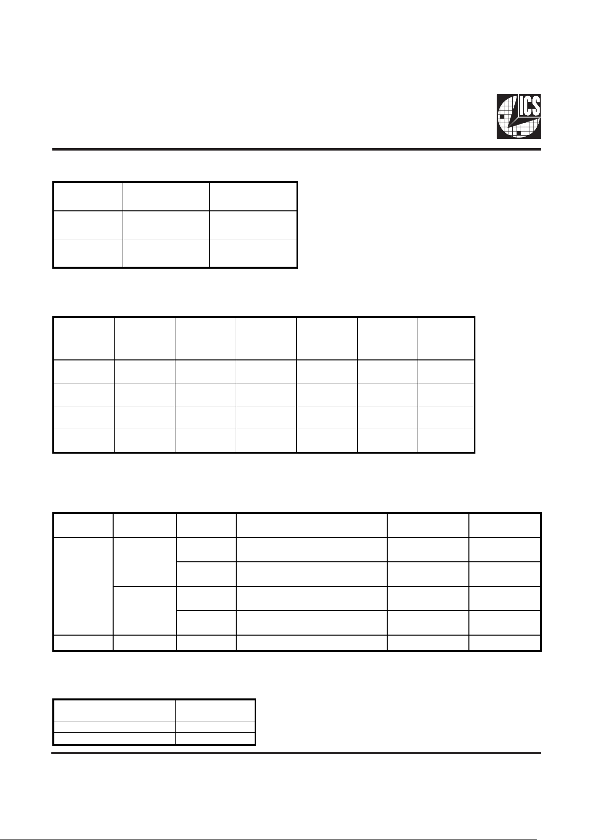
Byte0: Functionality and Frequency Select Register
Serial Configuration Command Bitmap
General I
2
C serial interface information
(default bits 0-3 to logic 0)
A. For the clock generator to be addressed by an I
2
C controller, the following address must be sent as a start sequence,
with an acknowledge bit between each byte.
B. The clock generator is a slave/receiver I
2
C component. It can "read back "(in Philips I2C protocol) the data stored in the
latches for verification. (set R/W# to 1 above). There is no BYTE count supported, so it does not meet the Intel SMB
PIIX4 protocol.
C. The data transfer rate supported by this clock generator is 100K bits/sec (standard mode)
D. The input is operating at 3.3V logic levels.
E. The data byte format is 8 bit bytes.
F. To simplify the clock generator I
2
C interface, the protocol is set to use only block writes from the controller. The bytes
must be accessed in sequential order from lowest to highest byte with the ability to stop after any complete byte has
been transferred. The Command code and Byte count shown above must be sent, but the data is ignored for those two
bytes. The data is loaded until a Stop sequence is issued.
G. The Fixed clocks 24, 48MHz are not addressable in the registers for Stopping. These outputs are always running, except
in Tristate Mode.
H. At power-on, all registers are set to a default condition. See Byte 0 detail for default condition, Bytes 1 through 5 default
to a 1 (Enabled output state)
Then Byte 0, 1, 2, etc in
sequence until STOP.
Byte 0, 1, 2, etc in sequence until STOP.
Clock Generator
Address (7 bits)
ACK
+ 8 bits dummy
command code
ACK
+ 8 bits dummy
Byte count
ACK
A(6:0) & R/W#
D2
(H)
Clock Generator
Address (7 bits)
ACK
Byte 0 ACK Byte 1 ACK
A(6:0) & R/W#
D3
(H)
I2C is a trademark of Philips Corporation
Note: PWD = Power-Up Default
Note 1. Default at Power-up will be for
latched logic inputs to define the
frequency. Bits 4, 5, 6 are default
to 000. If bit 3 is written to a 1 to
use Bits 6:4, then these should be
defined to the desired frequency at
same write cycle.
Bit Desc ription PWD
Bit 7
0 - ±1.5% Spread Spectrum Modulation
1 - ±0.5% Spre ad Spectrum M odulation
0
Bit 6:4
Bit6 B it5 Bit4
111
110
101
100
011
010
001
000
CPU clock
66.8
60.0
75.0
83.3
68.5
83.3
75.0
50.0
PCI
33.4(1/2 CPU)
30.0 (1/2 CPU)
37.5 (1/2 CPU)
33.3
34.5 (1/2 CPU)
41.65 (1/2 CPU )
32.0
25.0 (1/2 CPU)
Note 1
Bit 3
0 - Frequency is selected by hardware select, Latched
Inputs
1 - Frequency is selected by Bit 6:4 (above)
0
Bit 2
0 - Spread Spectrum center spread type. (default)
1 - Spread Spectrum down spread type.
0
Bit 1
Bit 0
Bit1
1
1
0
0
Bit0
1 - Tri-State
0 - Spread Spectrum Ena ble
1 - Testmode
0 - Normal Operation
0
0

7
ICS9150-04
Select Functions
Notes:
1. REF is a test clock on the X1 inputs during test mode.
FUNCTION
DESCRIPTION
OUTPUTS
CPU
PCI,
PCI_F
SDRAM REF IOAPIC
Tri - State Hi-ZHi-ZHi-ZHi-ZHi-Z
Test Mode TCLK/2
1
TCLK/4
1
TCLK/2
1
TCLK
1
TCLK
1
Byte 1: CPU Clock Register
Notes: 1 = Enabled; 0 = Disabled, outputs held low
Byte 2: PCICLK Clock Register
Byte 4: SDRAM Clock Register
Notes: 1 = Enabled; 0 = Disabled, outputs held low
Notes: 1 = Enabled; 0 = Disabled, outputs held low
BIT PIN# PWD DESCRIPTION
Bit 7 - 1 Reserve d
Bit 6 - 1 Reserve d
Bit 5 - 1 Reserve d
Bit 4 46 1 CPUCLK4 (Act/Inact)
Bit 3 48 1 CPUCLK3 (Act/Inact)
Bit 2 49 1 CPUCLK2 (Act/Inact)
Bit 1 51 1 CPUCLK1 (Act/Inact)
Bit 0 52 1 CPUCLK0 (Act/Inact)
Byte 3: SDRAM Clock Register
Notes: 1 = Enabled; 0 = Disabled, outputs held low
BIT PIN# PW D DESC RIPTION
Bit 7 35 1 SDRAM7 (Act/Ina ct)
Bit 6 36 1 SDRAM6 (Act/Ina ct)
Bit 5 38 1 SDRAM5 (Act/Ina ct)
Bit 4 39 1 SDRAM4 (Act/Ina ct)
Bit 3 41 1 SDRAM3 (Act/Ina ct)
Bit 2 42 1 SDRAM2 (Act/Ina ct)
Bit 1 44 1 SDRAM1 (Act/Ina ct)
Bit 0 45 1 SDRAM0 (Act/Ina ct)
BIT PIN# PWD DESCRIPTION
Bit 7 - 1 Reserved
Bit 6 8 1 PCICLK_F (Act/Inact)
Bit 5 1 6 1
PCICLK5 (Act/Inact)
Desktop Mode Only
Bit 4 14 1 PCICLK4 (Act/Inact)
Bit 3 13 1 PCICLK3 (Act/Inact)
Bit 2 12 1 PCICLK2 (Act/Inact)
Bit 1 11 1 PCICLK1 (Act/Inact)
Bit 0 9 1 PCICLK0 (Act/Inact)
BIT PIN# PWD DESCRIPTION
Bit 7 24 1 SDRA M15 (Act/Inact)
Bit 6 25 1 SDRA M14 (Act/Inact)
Bit 5 32 1 SDRA M13 (Act/Inact)
Bit 4 33 1 SDRA M12 (Act/Inact)
Bit 3 18 1 SDRA M11 (Act/Inact)
Bit 2 19 1 SDRA M10 (Act/Inact)
Bit 1 21 1 SDRA M9 (Act/Inact)
Bit 0 22 1 SDRA M8 (Act/Inact)

8
ICS9150-04
ICS9150-04 Power Management Requirements
Notes.
1. Clock on latency is defined from when the clock enable goes active to when the first valid clock comes out of the device.
2. Clock off latency is defined from when the clock enable goes inactive to when the last clock is driven low out of the device.
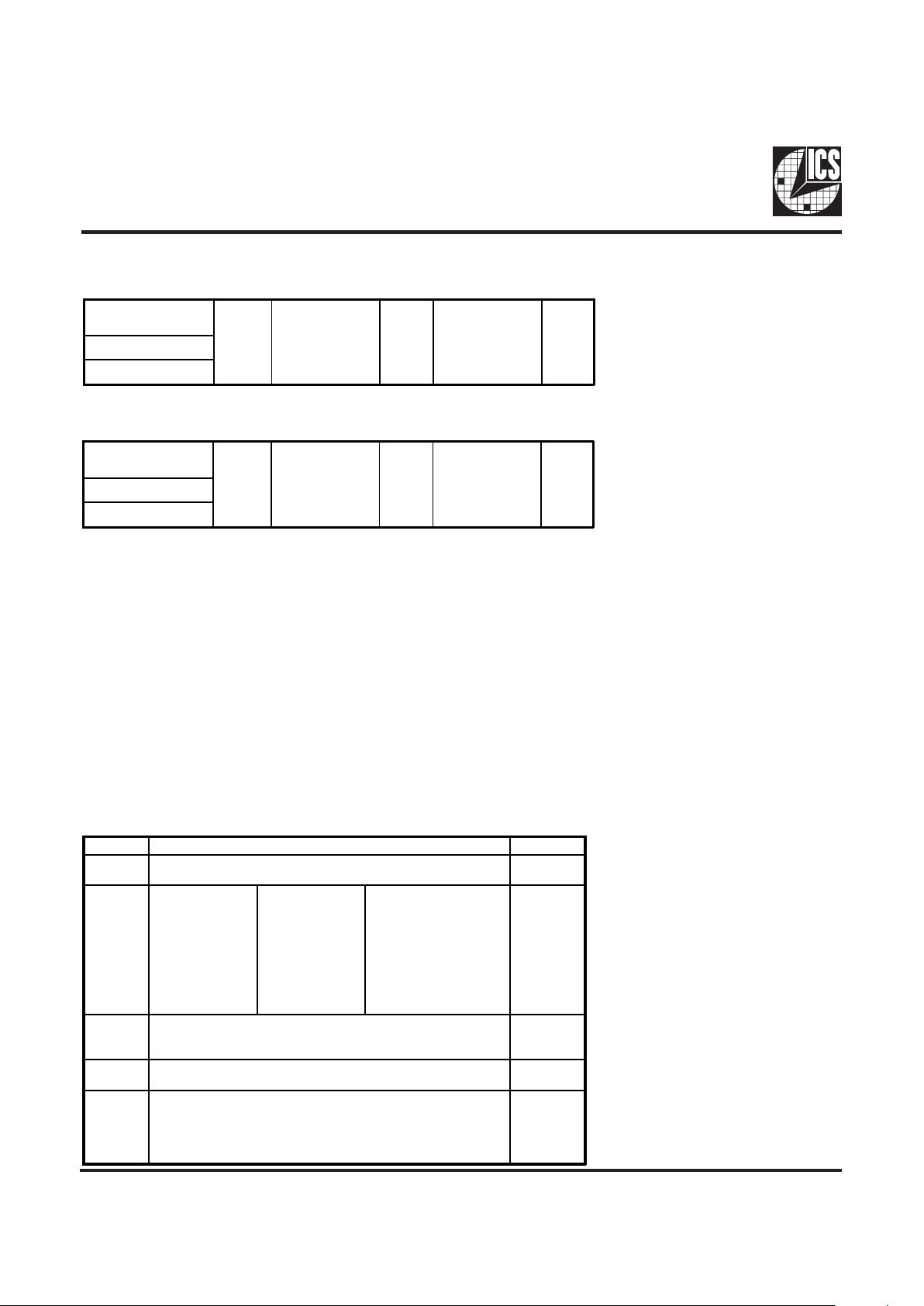
SIGNAL SI GNAL STATE
Latency
No. of rising edges of free
running PCICLK
CPU_ STOP# 0 (Disabled)
2
1
1 (Enabled)
1
1
PCI_STOP# 0 (Di sabled)
2
1
1 (Enabled)
1
1
Byte 5: Peripheral Clock Register
Notes: 1 = Enabled; 0 = Disabled, outputs held low
BIT PIN# PWD DESCRIPTION
Bit 7 - 1 Reserved
Bit 6 2 1 IOAPIC2 (Act/Inact)
Bit 5 54 1
IOAPIC1 (A ct/Inact)
Desktop Mode Only
Bit 4 55 1 IOAPIC0 (Act/Inact)
Bit 3 - 1 Reserved
Bit 2 - 1 Reserved
Bit 1 - 1 Reserved
Bit 0 3 1 REF0 (Act/Inact)
Byte 6: Peripheral Clock Register
Notes:
1. Byte 6 is reserved by Integrated Circuit Systems for
future applications.
BIT PIN# PWD DESCRIPTION
Bit 7 - 1 Reserved
Bit 6 - 1 Reserved
Bit 5 - 1 Reserved
Bit 4 - 1 Reserved
Bit 3 - 1 Reserved
Bit 2 - 1 Reserved
Bit 1 - 1 Reserved
Bit 0 - 1 Reserve

9
ICS9150-04
CPU_STOP# Timing Diagram
CPUSTOP# is an asychronous input to the clock synthesizer. It is used to turn off the CPUCLKs for low power operation.
CPU_STOP# is synchronized by the ICS9150-04. The minimum that the CPUCLK is enabled (CPU_STOP# high pulse) is 100
CPUCLKs. All other clocks will continue to run while the CPUCLKs are disabled. The CPUCLKs will always be stopped in a low
state and start in such a manner that guarantees the high pulse width is a full pulse. CPUCLK on latency is less than 4 CPUCLKs
and CPUCLK off latency is less than 4 CPUCLKs.
Notes:
1. All timing is referenced to the internal CPUCLK.
2. CPU_STOP# is an asynchronous input and metastable conditions may exist. This signal is synchronized to the
CPUCLKs inside the ICS9150-04.
3. All other clocks continue to run undisturbed.
4. PCI_STOP# is shown in a high (true) state.
Notes:
1. All timing is referenced to the Internal CPUCLK (defined as inside the ICS9150 device.)
2. PCI_STOP# is an asynchronous input, and metastable conditions may exist. This signal is required to be synchronized
inside the ICS9150.
3. All other clocks continue to run undisturbed.
4. CPU_STOP# is shown in a high (true) state.
PCI_STOP# Timing Diagram
PCI_STOP# is an asynchronous input to the ICS9150-04. It is used to turn off the PCICLK (0:5) clocks for low power operation.
PCI_STOP# is synchronized by the ICS9150-04 internally. The minimum that the PCICLK (0:5) clocks are enabled (PCI_STOP#
high pulse) is at least 10 PCICLK (0:5) clocks. PCICLK (0:5) clocks are stopped in a low state and started with a full high pulse
width guaranteed. PCICLK (0:5) clock on latency cycles are only one rising PCICLK clock off latency is one PCICLK clock.

10
ICS9150-04
Pins 2, 8, 9, 29 and 30 on the ICS9150-04 serve as dual
signal functions to the device. During initial power-up, they
act as input pins. The logic level (voltage) that is present on
these pins at this time is read and stored into a 4-bit internal
data latch. At the end of Power-On reset, (see AC
characteristics for timing values), the device changes the
mode of operations for these pins to an output function. In
this mode the pins produce the specified buffered clocks to
external loads.
To program (load) the internal configuration register for
these pins, a resistor is connected to either the VDD (logic 1)
power supply or the GND (logic 0) voltage potential. A 10
Kilohm(10K) resistor is used to provide both the solid CMOS
programming voltage needed during the power-up
programming period and to provide an insignificant load on
the output clock during the subsequent operating period.
Figs. 1 and 2 show the recommended means of implementing
this function. In Fig. 1 either one of the resistors is loaded
onto the board (selective stuffing) to configure the device’s
internal logic. Figs. 2a and b provide a single resistor
loading option where either solder spot tabs or a physical
jumper header may be used.
Shared Pin Operation Input/Output Pins
Fig. 1
These figures illustrate the optimal PCB physical layout
options. These configuration resistors are of such a large
ohmic value that they do not effect the low impedance clock
signals. The layouts have been optimized to provide as little
impedance transition to the clock signal as possible, as it
passes through the programming resistor pad(s).

11
ICS9150-04
Fig. 2a
Fig. 2b

12
ICS9150-04
Absolute Maximum Ratings
Supply Voltage . . . . . . . . . . . . . . . . . . . . . . . . . . . . 7.0 V
Logic Inputs . . . . . . . . . . . . . . . . . . . . . . . . . . . . . . GND 0.5 V to V
DD
+0.5 V
Ambient Operating Temperature . . . . . . . . . . . . . 0°C to +70°C
Storage Temperature . . . . . . . . . . . . . . . . . . . . . . . 65°C to +150°C
Stresses above those listed under Absolute Maximum Ratings may cause permanent damage to the device. These ratings are
stress specifications only and functional operation of the device at these or any other conditions above those listed in the
operational sections of the specifications is not implied. Exposure to absolute maximum rating conditions for extended periods
may affect product reliability.
Electrical C haracteristi cs - Input/ Supply/C om m on Output Parameters
TA = 0 - 70C; Supply Voltage VDD = V
DDL
= 3 .3 V + / -5% (unle ss oth e rwis e stated)
PARA METER SY MBOL COND ITI O NS MIN TYP MAX UNITS
In put High Voltage V
IH
2V
DD
+0.3 V
Input Low V olta ge V
IL
VSS-0.3 0.8 V
Input High Current I
IH
VIN = V
DD
0.1 5
µ
A
Inpu t Low C urrent I
IL1
VIN = 0 V; Inputs with no pull -up r e sis tors -5 2.0
µ
A
Inpu t Low C urrent I
IL2
VIN = 0 V; Inputs with pull -up r e sis tors -200 -100
µ
A
Operating I
DD3.3OPCL
= 0 pF; Sele c t @ 66MHz 135 160 m A
Suppl y C urrent
Input frequency F
i
VDD = 3 .3 V; 14.318 MHz
In put C apacit a n c e
1
C
IN
Logic Inputs 5 pF
C
INX
X 1 & X2 pins 27 36 45 pF
Tr ansition Time
1
T
trans
To 1s t c rossing of targe t Freq. 2 ms
Settling Tim e
1
T
s
From 1st c rossing t o 1% target Freq. ms
Clk Stabiliza tion
1
T
STAB
From VDD = 3.3 V to 1% t a rget Freq. 2 ms
Skew
1
T
CPU-SDRAM1VT
= 1.5 V; VDD = 3.3; 200 350 ps
66.8 MHz; SDRAM Le a ds
T
CPU-PCI1VT
= 1.5 V ;
12.24 ns
1
G ua renteed by de sign, not 100% t e sted i n production.
Electr ical Character ist ics - Input/Suppl y/Comm on O utput Parameter s
TA = 0 - 70C; S uppl y Voltage VDD = V
DDL
= 3. 3 V +/-5% (unless otherwise stated)
PARAMETER SYMBOL CONDI TIONS MIN TYP MAX UNITS
I
DD2.5OP
CL = 0 pF; Sel ect @ 66M 5 30 mA
T
CPU-SDRAM2
VT = 1.5V; VTL = 1. 25V ; V
DDL
= 2. 5;
66.8MHz; SDRAM Leads
500 800 ps
T
CPU-PCI2VT
= 1.5V; VTL = 1. 25V ; CPU Leads 1 2.5 4 ns
1
Guarenteed by design, not 100% t est ed in produc tion.
Operating S upply
Current Sk ew
1

13
ICS9150-04
Ele ctrical C h aracteri stics - C P U
TA = 0 - 70C; VDD = 3.3 V +/-5%, V
DDL
= 2.5 V +/-5%; CL = 10 - 20 pF ( unl ess otherwise sta t ed)
PARAMETER SY MBOL COND ITI O NS MIN TYP MAX UN ITS
Output Impedance
RDSP2B
1
VO = VDD*(0.5) 10 25
Ω
Output Impedance
RDS N2B
1
VO = VDD*(0.5) 10 25
Ω
Output High Voltage VOH2B I
OH
= -8 mA 2 2.2 V
Output Low Voltage VOL2B I
OL
= 12 mA 0.3 0.4 V
Ou tput High Current IOH 2B V
OH
= 2.0 V -20 -16 mA
Output Low Current IOL2B V
OL
= 0.7 V 19 26 mA
Rise Time
tr2B
1
VOL = 0.4 V, VOH = 2.0 V 2.5 3 ns
Fall Time
tf2B
1
VOH = 2.0 V, VOL = 0.4 V 1.6 2 ns
Duty Cycle
dt2B
1
VT = 1.25 V 43 46 55 %
Skew
tsk2B
1
VT = 1.25 V 60 250 ps
Jitter, Single Edge
Displacement
2
tjsed2B
1
VT = 1.25 V 200 300 ps
Jitter, One Sigma
tj1s2B
1
VT = 1.25 V 80 150 ps
Jitter , A bs olute
tjabs2B
1
VT = 1.25 V
-30 0 80 300 ps
1
G uara n t e ed by design, not 100% tested in p roduction.
2 Edge di splac eme nt o f a perio d relative to a 1 0-clock-cycle rolling average pe riod.
Ele ctrical C h aracteristic s - CPU
TA = 0 - 70C; VDD = V
DDL
= 3 .3 V +/-10%; CL = 10 - 20 pF (unless otherw ise stated)
PARA METER SYMBOL CON D ITI O N S MIN TYP MAX UNITS
Output Impedance R
DSP2A
1
VO = VDD*(0.5) 10 20
Ω
Output Impedance R
DSN2 A
1
VO = VDD*(0.5) 10 20
Ω
Out put High Volta ge V
OH2AIOH
= -28 mA 2. 5 2.6 V
Output Low Voltage V
OL2AIOL
= 27 mA 0.3 5 0.4 V
Output High Current I
OH2A
VOH = 2 .0 V - 29 -23 mA
Output Low Current I
OL2A
VOL = 0.8 V 33 37 mA
Rise Tim e t
r2A
1
VOL = 0.4 V, VOH = 2 .4 V 1.9 2. 5 ns
Fall T ime t
f2A
1
VOH = 2.4 V, VOL = 0.4 V 1.4 2 ns
Duty Cycle d
t2A
1
VT = 1.5 V 45 48 55 %
Skew t
sk2A
1
VT = 1.5 V 80 250 ps
Jitter, Single Edge
Displacement
2
tjsed2A
1
VT = 1.25 V 200 250 ps
Jitter, One Sigma t
j1s2A
1
VT = 1.5 V 60 150 ps
Jitter , Abs olute
t
jabs2A
1
VT = 1.5 V
- 300 200 300 ps

14
ICS9150-04
Elect ri cal C haracteri st ics - PCI
TA = 0 - 70C; VDD = V
DDL
= 3.3 V + /-10%; CL = 30 pF (unless otherwise s tated)
PARAMETER SYMBOL CONDITIONS MIN TYP MAX UNITS
O ut p ut Impedan c e R
DSP1
1
VO = VDD*(0.5) 12 55
Ω
O ut p ut Impedan c e R
DSN1
1
VO = VDD*(0.5) 12 55
Ω
Output High Voltage V
OH1IOH
= -28 mA 2.4 3 V
Output Low Voltage V
OL1IOL
= 23 mA 0.2 0.4 V
Output High Current I
OH1
VOH = 2.0 V -60 -40 mA
Output Low Current I
OL1
VOL = 0.8 V 41 50 mA
Rise Tim e t
r1
1
VOL = 0.4 V, VOH = 2. 4 V 1.4 2 ns
Fa ll T im e t
f1
1
VOH = 2.4 V , VOL = 0. 4 V 1.3 2 ns
Duty Cycle d
t1
1
VT = 1.5 V 45 49 55 %
Skew t
sk1
1
VT = 1.5 V 80 500 ps
Jitter, One Sigma
1
t
j1s1
VT = 1.5 V, synchronous, excl uding sele c t 4 3 0 15 0 ps
t
j1s1a
VT = 1.5 V, synchronous, selec t 4 385 55 0 ps
t
j1s1b
VT = 1.5 V, asynchronous, select 1 175 250 ps
Jitter, Absolute
1
t
jabs1
VT = 1.5 V, synchronous, excl uding sele c t 4 -250 100 250 ps
t
j1s1a
VT = 1.5 V, synchronous, select 4 -700 510 700 ps
t
jabs1bVT
= 1 . 5 V, asynchronous, select 1
-500 390 500 ps
1
G uarenteed by des ign, not 100% tes ted in production.

15
ICS9150-04
Ele ctri cal Characteristics - S DRAM
TA = 0 - 70C; VDD = V
DDL
= 3 .3 V + / -10%; CL = 20 - 30 pF ( unl e ss ot he rwis e sta t ed)
PARAMETER SYMBOL COND ITI ON S MIN TYP MAX UNI TS
O utp ut Impedanc e
R
DSP3
1
VO = VDD*(0.5) 10 24
Ω
O utp ut Impedanc e
R
DSN3
1
VO = VDD*(0.5) 10 24
Ω
Output High Voltage V
OH3IOH
= -28 mA (except SD R AM12,13) 2. 4 3 V
V
OH3aIOH
= -16 mA (SDRA M12,13) 2.4 2.6 V
Output Low Voltage V
OL3IOL
= 23 m A (except SDRAM12,13) 0.2 0.4 V
V
OL3aIOL
= 9 mA ( SDRAM12, 13) 0. 3 0.4 V
O utput High Current I
OH3
VOH = 2.0 V ( except SDRAM12, 13) -60 -40 mA
I
OH3a
VOH = 2.0 V (SDRAM12,13) -32 -22 mA
Output Low Current I
OL3
VOL = 0.8 V ( except SDRAM12, 13) 41 50 mA
I
OL3a
VOL = 0.8 V ( SDRAM12, 1 3) 16 25 mA
T
r3
1
VOL = 0.4 V, VOH = 2.4
(e xc e pt S DRAM12,13)
1.2 2 ns
T
r3a
1
VOL = 0.4 V, VOH = 2.4 V ( SDRAM12, 1 3) 2.5 4 ns
T
f3
1
VOH = 2.4 V, VOL = 0.4
(e xc e pt S DRAM12,13)
1.1 2 ns
T
f3a
1
VOH = 2.4 V, VOL = 0.4 V (SDRAM12,13) 2.7 4 ns
Duty Cycle
D
t3
1
VT = 1.5 V 45 51 57 %
Skew
T
sk3
1
VT = 1.5 V (exce pt SDRAM12, 13 ) 285 500 ps
Jitter, One Sigma
T
j
1s3
1
VT = 1.5 V 50 150 ps
Jitter, Absolute
T
j
abs3
1
VT = 1.5 V -250 - 250 ps
1
G ua ranteed by de sign, not 100% tested in production .
Rise Time
Fall Time

16
ICS9150-04
Ele ctri cal Characteristics - IOAPIC
TA = 0 - 70C; VDD = 3.3 V +/-5%, V
DDL
= 2.5 V +/-5%; CL = 10 - 20 pF ( unl ess otherwis e state d )
PARAMETER SYMBOL CON DI TIO N S MIN TYP MAX U NI TS
O utp ut Impedanc e R
DSP4B
1
VO = VDD*(0.5) 10 30
Ω
O utp ut Impedanc e R
DSN4 B
1
VO = VDD*(0.5) 10 30
Ω
Output High Voltage V
OH4\BIOH
= -8 mA 2 2.1 V
Output Low Voltage V
OL4BIOL
= 12 m A 0.3 0.4 V
O utput High Current I
OH4B
VOH = 1.7 V -20 -16 mA
Output Low Current I
OL4B
VOL = 0.7 V 19 26 mA
Rise Time t
r4B
1
VOL = 0.4 V, VOH = 2.0 V 1.9 4 ns
Fall Time t
f4B
1
VOH = 2.0 V, VOL = 0.4 V 1.5 3.2 ns
Duty Cycle d
t4B
1
VT = 1.25 V 455355%
Skew t
sk4B
1
VT = 1.25 V 60 250 ps
Jitter, One Sigma t
j1s4B
1
VT = 1.25 V 1 3 %
Jitter, Absolute
t
jabs4B
1
VT = 1.25 V
-5 5 %
1
G ua ranteed by de sign, not 100% t e sted i n production.
Electrical Characteristics - IOAPIC
TA = 0 - 70C; VDD = V
DDL
= 3 .3 V + / -10%; CL = 10 - 20 pF ( unl e ss ot he rwis e sta t ed)
PARAMETER SYMBOL CONDI TIO N S MIN TYP MAX UNITS
O utpu t Frequenc y F
O4
14.318 MHz
O utp ut Impedanc e R
DSP4A
1
VO = VDD*(0.5) 10 30
Ω
O utp ut Impedanc e R
DSN4A
1
VO = VDD*(0.5) 10 30
Ω
Output High Voltage V
OH4AIOH
= -16 mA 2.4 2.6 V
Output Low Voltage V
OL4AIOL
= 9 m A 0.3 0.4 V
O utput High Current I
OH4A
VOH = 2.0 V -32 -22 mA
Output Low Current I
OL4A
VOL = 0.8 V 16 25 m A
Rise Time t
r4A
1
VOL = 0.4 V, VOH = 2.4 V 1.8 4 ns
Fall Time t
f4A
1
VOH = 2.4 V, VOL = 0.4 V 2.2 4 ns
Duty Cycle d
t4A
1
VT = 1.5 V 45 53 57 %
Skew t
sk4A
1
VT = 1.25 V 60 250 ps
Jitter, One Sigma t
j1s4A
1
VT = 1.5 V 1 3 %
Jitter, Absolute
t
jabs4A
1
VT = 1.5 V
-5 - 5 %
1
G ua ranteed by de sign, not 100% tested in production.

17
ICS9150-04
Ele ctrica l Charact eristics - 24MHz, 48MHz, REF0
TA = 0 - 70C; VDD = V
DDL
= 3 .3 V + / -10%; CL = 10 -20 pF ( unl e ss otherw i se s t a t ed)
PARAMETER SYMBOL COND ITI ON S MIN TYP MAX UN I TS
O utpu t Frequenc y F
O24M
24 MH z
O utpu t Frequenc y F
O48M
48 MH z
O utpu t Frequenc y F
OREF
14.318 MHz
O utp ut Impedanc e R
DSP5
1
VO = VDD*(0.5) 20 60
Ω
O utp ut Impedanc e R
DSN5
1
VO = VDD*(0.5) 20 60
Ω
Output High Voltage V
OH5IOH
= -16 mA 2.4 2.6 V
Output Low Voltage V
OL5IOL
= 9 mA 0.3 0.4 V
O utput High Current I
OH5
VOH = 2.0 V -32 -22 mA
Output Low Current I
OL5
VOL = 0.8 V 16 25 mA
Rise Time t
r5
1
VOL = 0.4 V, VOH = 2.4 V 1.7 4 ns
Fall Time t
f5
1
VOH = 2.4 V, VOL = 0.4 V 2.1 4 ns
Duty Cycle d
t5
1
VT = 1.5 V 45 54 57 %
Jitter, One Sigma t
j1s5
1
VT = 1.5 V 1 3 %
Jitter, Absolute
t
jabs5
1
VT = 1.5 V
-5 - 5 %
1
G ua ranteed by de sign, not 100% t e sted i n production.

18
ICS9150-04
General Layout Precautions:
1) Use a ground plane on the top layer
of the PCB in all areas not used by
traces.
2) Make all power traces and vias as
wide as possible to lower inductance.
Notes:
1 All clock outputs should have series
terminating resistor. Not shown in all
places to improve readibility of
diagram
2 Optional EMI capacitor should be
used on all CPU, SDRAM, and PCI
outputs.
3 Optional crystal load capacitors are
recommended.
Capacitor Values:
C1, C2 : Crystal load values determined by user
C3 : 100pF ceramic
All unmarked capacitors are 0.01µF ceramic

19
ICS9150-04
SSOP Package
Ordering Information
ICS9150F-04
Pattern Number (2 or 3 digit number for parts with ROM code patterns)
Package Type
F=SSOP
Device Type (consists of 3 or 4 digit numbers)
Prefix
ICS, AV = Standard Device
Example:
ICS XXXX F - PPP
SYMBOL C OMMON DIMENSIONS VARIATIONS D N
MIN. NOM. MAX. MIN. NOM. MAX.
A .095 .101 .110 AC .620 .625 .630 48
A1 .008 .012 .016 AD .720 .725 .730 56
A2 .088 .090 .092
B .008 .010 .0135
C.005- .010
D See Variations
E .292 .296 .29 9
e0.025 BSC
H .400 .406 .410
h .010 .013 .016
L .024 .032 .040
N See Variations
∝
0° 5° 8°
X .085 .093 .100
ICS reserves the right to make changes in the device data identified in this
publication without further notice. ICS advises its customers to obtain the latest
version of all device data to verify that any information being relied upon by the
customer is current and accurate.
 Loading...