

Integrated
Circuit
Systems, Inc.
General Description Features
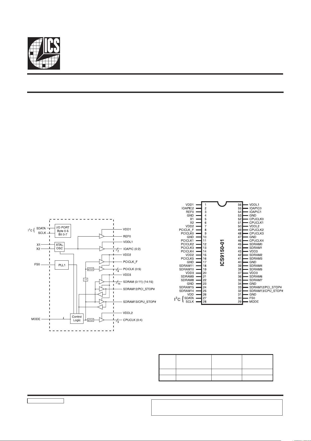
ICS9150-01
Block Diagram
Pentium is a trademark of Intel Corporation
Pentium Pro™ and SDRAM Frequency Generator
9150-01 RevE 4/25/01
Pin Configuration
The ICS9150-01 generates all clocks required for high speed
RISC or CISC microprocessor systems such as Intel
PentiumPro. Two different reference frequency multiplying
factors are externally selectable with smooth frequency
transitions. An output enable is provided for testability.
High drive PCICLK and SDRAM outputs typically provide
greater than 1 V/ns slew rate into 30 pF loads. CPUCLK
outputs typically provide better than 1V/ns slew rate into
20 pF loads while maintaining 50
±
5% duty cycle. The REF
clock outputs typically provide better than 0.5V/ns slew rates.
• Generates five processor, six bus, one 14.31818MHz
and 16 SDRAM clocks.
• Synchronous clocks skew matched to 250 ps window
on PCLKs and 500ps window on BCLKs
• Test clock mode eases system design
• Selectable multiplying ratios
• Custom configurations available
• Output frequency ranges to 100 MHz (depending on
option)
• 3.0V – 3.7V supply range
• PC serial configuration interface
• Power Management Control Input pins
• 56-pin SSOP package
56-Pin SSOP
Functionality
0SF
,KLCUPC
MARDS
)zHM(
FER,1X
)zHM(
KLCICP
)zHM(
00.06813.4103
16.66813.413.33
ICS reserves the right to make changes in the device data identified in this
publication without further notice. ICS advises its customers to obtain the latest
version of all device data to verify that any information being relied upon by the
customer is current and accurate.
2
ICS9150-01
Pin Descriptions
Power Groups
VDD = Supply for PLL core
VDD1 = REF 0, X1, X2
VDD2 = PCICLK_F, PCICLK (0:5)
VDD3 = SDRAM (0:11) (14:15), SDRAM13/CPU_STOP#, SDRAM12/PCI_STOP#
VDDL1 = IOAPIC (0:2)
VDDL2 = CPUCLK (0:4)
REBMUNNIPEMANNIPEPYTNOITPIRCSED
30FERTUO.stuptuokcolcecnereferzHM813.41
,13,32,71,01,4
35,74,04,43
DNGRWP.dnuorG
51XNI.pacdaollanretnisaH.tupnizHM813.41
62XTUO1XotrotsiserkcabdeefdnapacdaollanretnisaH.tuptuolatsyrC
92EDOMNI
,serutaeftnemeganamrewopgnilbanerofniptcelesedoM
.pullupsah
8F_KLCICPTUO.0=#POTS_ICPgnirudkcolcSUBgninnureerF
31,21,11,9
,4161
)5:0(KLCICPTUO.stuptuokcolcSUB
030SFNI
kcolcMARDS/UPC.zHM06rozHM6.66gnilbanerofniptceleS
ycneuqerf
72ATADSNI.tropgifnoclairesrofniatadlaireS
82KLCSNI.tropgifnoclairesroftupnikcolC
,62,02,51,7,1
34,73
,1DDV,2DDV
3DDV,DDV
RWP.noitcnufrofspuorgrewopees,ylppusrewopV3.3lanimoN
65,051LDDV,2LDDVRWP
V3.3ro5.2rehtie,ylppusrewopreffubkcolcCIPAOIdnaUPC
.lanimon
,42,22,12,91,81
,63,53,33,23,52
,44,24,14,93,83
54
)11:0(MARDS
)51:41(
TUO)zHM6.66/06(skcolcMARDS
55,45,2)2:0(CIPAOITUO1LDDVybderewoP)zHM81813.41(.tuptuokcolcCIPAOI
25,15,94,84,64)4:0(KLCUPCTUO)zHM6.66ro06(2LDDVybderewoP.skcolctuptuOUPC
23
31MARDSTUO)zHM6.66/06(kcolcMARDS
#POTS_UPCNI.wolnehwlevel"0"cigoltaskcolcKLCUPCstlaH
33
21MARDSTUO)zHM6.66/06(kcolcMARDS
#POTS_ICPNI.wolnehwlevel"0"cigolta)5:0(KLCICPstlaH
3
ICS9150-01
Power-On Conditions
Example:
a) if MODE = 1, pins 33 and 32 are configured as SDRAM12, and SDRAM13 respectively.
b) if MODE = 0, pins 33 and 32 are configured as PCI_STOP#, and CPU_STOP# respectively.
Power-On Default Conditions
At power-up and before device programming, all clocks will default to an enabled and “on” condition. The frequencies that are then
produced are on the FS and MODE pin as shown in the table below.
KCOLC PU-REWOPTANOITIDNOCTLUAFED
0FERzHM81813.41
)2:0(CIPAOIzHM81813.41
#06/66LESEDOM#NIPNOITPIRCSEDNOITCNUF
11
64,84,94,15,25sKLCUPCelbasid/elbanegifnoclaires/w-zHM6.66
,93,14,24,44,54
,12,22,53,63,83
,52,23,33,81,91
42
MARDSstuptuoMARDSllA-zHM6.66
,41,31,21,11,9
8,61
sKLCICPelbasid/elbanegifnoclaires/w-zHM3.33
01
64,84,94,15,25sKLCUPCelbasid/elbanegifnoclaires/w-zHM06
,93,14,24,44,54
,12,22,53,63,83
,52,23,33,81,91
42
MARDSelbasid/elbanegifnoclaires/w-zHM06
,41,31,21,11,9
8,61
sKLCICPelbasid/elbanegifnoclaires/w-zHM03
1
0
64,84,94,15,25sKLCUPCelbasid/elbanegifnoclaires/w-zHM6.66
,93,14,24,44,54
,12,22,53,63,83
42,52,81,91
MARDSstuptuoMARDSllA-zHM6.66
33#POTS_ICPwolnehwdeppotsskcolc)5:0(ICP,tnemeganaMrewoP
23#POTS_UPCwolnehwdeppotsskcolcUPC,nemeganaMrewoP
00
64,84,94,15,25sKLCUPCelbasid/elbanegifnoclaires/w-zHM06
,93,14,24,44,54
,12,22,53,63,83
42,52,81,91
MARDSelbasid/elbanegifnoclaires/w-zHM06
33#POTS_ICPwolnehwdeppotsskcolc)5:0(ICP,tnemeganaMrewoP
23#POTS_UPCwolnehwdeppotsskcolcUPC,nemeganaMrewoP

4
ICS9150-01
VDD(1,2,3)
This is the power supply to the internal core logic of the device as well
as the clock output buffers for REF(0:1), PCICLK, and
SDRAM(0:7).
This pin operates at 3.3V volts. Clocks from the listed buffers that it
supplies will have a voltage swing from Ground to this level. For the
actual guaranteed high and low voltage levels for the Clocks, please
consult the DC parameter table in this data sheet.
VDDL1,2
This is the power supplies for the CPUCLK and IOAPCI output
buffers. The voltage level for these outputs may be 2.5 or 3.3volts.
Clocks from the buffers that each supplies will have a voltage swing
from Ground to this level. For the actual Guaranteed high and low
voltage levels of these Clocks, please consult the DC parameter
table in this Data Sheet.
GND
This is the power supply ground (common or negative) return pin for
the internal core logic and all the output buffers.
X1
This input pin serves one of two functions. When the device is used
with a Crystal, X1 acts as the input pin for the reference signal that
comes from the discrete crystal. When the device is driven by an
external clock signal, X1 is the device input pin for that reference
clock. This pin also implements an internal Crystal loading capacitor
that is connected to ground. See the data tables for the value of this
capacitor.
X2
This Output pin is used only when the device uses a Crystal as the
reference frequency source. In this mode of operation, X2 is an
output signal that drives (or excites) the discrete Crystal. The X2 pin
will also implement an internal Crystal loading capacitor that is
connected to ground. See the Data Sheet for the value of this
capacitor.
CPUCLK (0:4)
These Output pins are the Clock Outputs that drive processor and
other CPU related circuitry that requires clocks which are in tight
skew tolerance with the CPU clock. The voltage swing of these
Clocks are controlled by the Voltage level applied to the VDDL2 pin
of the device. See the Functionality Table for a list of the specific
frequencies that are available for these Clocks and the selection
codes to produce them.
SDRAM(0:15)
These Output Clocks are use to drive Dynamic RAM’s and are low
skew copies of the CPU Clocks. The voltage swing of the
SDRAM’s output is controlled by the supply voltage that is applied
to VDD3 of the device, operates at 3.3 volts.
IOAPIC (0:2)
These Outputs are fixed frequency Output Clocks that run at the
Reference Input (typically 14.31818MHz) . Its voltage level swing
is controlled by VDDL1 and may operate at 2.5 or 3.3volts.
Technical Pin Function Descriptions
REF0
The REF Output is a fixed frequency Clock that runs at the same
frequency as the Input Reference Clock X1 or the Crystal (typically
14.31818MHz) attached across X1 and X2.
PCICLK_F
This Output is equal to PCICLK(0:5) and is FREE RUNNING, and
will not be stopped by PCI_STP#.
PCICLK (0:5)
These Output Clocks generate all the PCI timing requirements for a
Pentium/Pro based system. They conform to the current PCI
specification. They run at 1/2 CPU frequency.
FS0
This Input pin controls the frequency of the Clocks at the CPU,
PCICLK and SDRAM output pins. If a logic “1” value is present on
this pin, the 66.6 MHz Clock will be selected. If a logic “0” is used,
the 60MHz frequency will be selected. (This is the Power Management
Mode)
MODE
This Input pin is used to select the Input function of the I/O pins.
An active Low will place the I/O pins in the Input mode and enable
those stop clock functions. (This is the Power Management Mode)
CPU_STOP#
This is a synchronous active Low Input pin used to stop the CPUCLK
clocks in an active low state. All other Clocks including SDRAM
clocks will continue to run while this function is enabled. The
CPUCLK’s will have a turn ON latency of at least 3 CPU clocks. This
input pin only valid when MODE=0 (Power Management Mode)
PCI_STOP#
This is a synchronous active Low Input pin used to stop the PCICLK
clocks in an active low state. It will not effect PCICLK_F nor any
other outputs. This input pin only valid when MODE=0 (Power
Management Mode)
I
2
C
The SDATA and SCLOCK Inputs are use to program the device. The
clock generator is a slave-receiver device in the I
2
C protocol. It will
allow read-back of the registers. See configuration map for register
functions. The I
2
C specification in Philips I2C Peripherals Data
Handbook (1996) should be followed.
5
ICS9150-01
Serial Configuration Command Bitmaps
Byte 0: Functional and Frequency Select Clock Register (default = 0)
TIB#NIPNOITPIRCSEDDWP
7tiB- devreseR0
6tiB- noitarepolamronrof0ebtsuM0
5tiB
-noitarepolamronrof0ebtsuM
0
-
epytslortnoC,murtcepSdaerpSnI
)daerpsnwod=1,deretnec=0(
4tiB
-noitarepolamronrof0ebtsuM
0
-
slortnoCslortnoC,murtcepSdaerpSnI
%gnidaerpS
)%6.0=1,%8.1=0(
3tiB- devreseR0
2tiB- devreseR0
1tiB
0tiB
-
1tiB
1
1
0
0
0tiB
etatS-irT-1
elbanEmurtcepSdaerpS-0
edomtseT-1
noitarepolamroN-0
0
0
General I2C serial interface information
A. For the clock generator to be addressed by an I2C controller, the following address must be sent as a start sequence, with
an acknowledge bit between each byte.
B. The clock generator is a slave/receiver I2C component. It can "read back "(in Philips I2C protocol) the data stored in the
latches for verification. (set R/W# to 1 above). There is no BYTE count supported, so it does not meet the Intel SMB
PIIX4 protocol.
C. The data transfer rate supported by this clock generator is 100K bits/sec (standard mode)
D. The input is operating at 3.3V logic levels.
E. The data byte format is 8 bit bytes.
F. To simplify the clock generator I2C interface, the protocol is set to use only block writes from the controller. The bytes
must be accessed in sequential order from lowest to highest byte with the ability to stop after any complete byte has
been transferred. The Command code and Byte count shown above must be sent, but the data is ignored for those two
bytes. The data is loaded until a Stop sequence is issued.
G. In the power down mode (PWR_DWN# Low), the SDATA and SCLK pins are tristated and the internal data latches
maintain all prior programming information.
H. At power-on, all registers are set to a default condition. See Byte 0 detail for default condition, Bytes 1 through 5 default
to a 1 (Enabled output state)
Then Byte 0, 1, 2, etc in
sequence until STOP.
Byte 0, 1, 2, etc in sequence until STOP.
rotareneGkcolC
)stib7(sserddA
KCA
ymmudstib8+
edocdnammoc
KCA
ymmudstib8+
tnuocetyB
KCA
#W/R&)0:6(A
2D)H(
rotareneGkcolC
)stib7(sserddA
KCA0etyBKCA1etyBKCA
#W/R&)0:6(A
3D)H(
Note: PWD = Power-Up Default
I2C is a trademark of Philips Corporation

6
ICS9150-01
Byte 1: CPU Clock Register
Select Functions
Notes:
1. REF is a test clock on the X1 inputs during test mode.
Notes: 1 = Enabled; 0 = Disabled, outputs held low
Byte 2: PCICLK Clock Register
Byte 4: SDRAM Clock Register
Notes: 1 = Enabled; 0 = Disabled, outputs held low
Notes: 1 = Enabled; 0 = Disabled, outputs held low
TIB#NIPDWPNOITPIRCSED
7tiB-1 devreseR
6tiB81 )tcanI/tcA(F_KLCICP
5tiB611 )tcanI/tcA(5KLCICP
4tiB411 )tcanI/tcA(4KLCICP
3tiB311 )tcanI/tcA(3KLCICP
2tiB211 )tcanI/tcA(2KLCICP
1tiB111 )tcanI/tcA(1KLCICP
0tiB91 )tcanI/tcA(0KLCICP
TIB#NIPDWPNOITPIRCSED
7tiB-1 devreseR
6tiB-1 devreseR
5tiB-1 devreseR
4tiB641 )tcanI/tcA(4KLCUPC
3tiB841 )tcanI/tcA(3KLCUPC
2tiB941 )tcanI/tcA(2KLCUPC
1tiB151 )tcanI/tcA(1KLCUPC
0tiB251 )tcanI/tcA(0KLCUPC
Byte 3: SDRAM Clock Register
Notes: 1 = Enabled; 0 = Disabled, outputs held low
NOITCNUF
NOITPIRCSED
STUPTUO
UPC
,ICP
F_ICP
MARDSFERCIPAOI
etatS-irTZ-iHZ-iHZ-iHZ-iHZ-iH
edoMtseT2/KLCT
1
4/KLCT
1
2/KLCT
1
KLCT
1
KLCT
1
TIB#NIPDWPNOITPIRCSED
7tiB531 )tcanI/tcA(7MARDS
6tiB631 )tcanI/tcA(6MARDS
5tiB831 )tcanI/tcA(5MARDS
4tiB931 )tcanI/tcA(4MARDS
3tiB141 )tcanI/tcA(3MARDS
2tiB241 )tcanI/tcA(2MARDS
1tiB441 )tcanI/tcA(1MARDS
0tiB541 )tcanI/tcA(0MARDS
TIB#NIPDWPNOITPIRCSED
7tiB421 )tcanI/tcA(51MARDS
6tiB521 )tcanI/tcA(41MARDS
5tiB231
)tcanI/tcA(31MARDS
ylnOpotkseD
4tiB331
)tcanI/tcA(21MARDS
ylnOpotkseD
3tiB811 )tcanI/tcA(11MARDS
2tiB911 )tcanI/tcA(01MARDS
1tiB121 )tcanI/tcA(9MARDS
0tiB221 )tcanI/tcA(8MARDS

7
ICS9150-01
Power Management
ICS9150-01 Power Management Requirements
Clock Enable Configuration
Full clock cycle timing is guaranteed at all times after the system has initially powered up except where noted. The first clock
pulse coming out of a stopped clock condition may be slightly distorted due to clock network charging circuitry. Board routing
and signal loading may have a large impact on the initial clock distortion also.
Notes.
1. Clock on latency is defined from when the clock enable goes active to when the first valid clock comes out of the device.
2. Clock off latency is defined from when the clock enable goes inactive to when the last clock is driven low out of the device.
Byte 5: Peripheral Clock Register
Notes: 1 = Enabled; 0 = Disabled, outputs held low
TIB#NIPDWPNOITPIRCSED
7tiB-1 devreseR
6tiB21 )tcanI/tcA(2CIPAOI
5tiB451 )tcanI/tcA(1CIPAOI
4tiB551 )tcanI/tcA(0CIPAOI
3tiB-1 devreseR
2tiB-1 devreseR
1tiB-1 devreseR
0tiB31 )tcanI/tcA(0FER
#POTS_UPC#POTS_ICPKLCUPCKLCICP
,skcolCrehtO
,MARDS
,FER
sCIPAOI
latsyrCsOCV
00 woLwoLgninnuRgninnuRgninnuR
01 woLzHM03/3.33gninnuRgninnuRgninnuR
10 zHM06/6.66woLgninnuRgninnuRgninnuR
11 zHM06/6.66zHM03/3.33gninnuRgninnuRgninnuR
LANGISETATSLANGIS
ycnetaL
gninnureerffosegdegnisirfo.oN
KLCICP
#POTS_UPC
)delbasiD(0
2
1
)delbanE(1
1
1
#POTS_ICP
)delbasiD(0
2
1
)delbanE(1
1
1
Byte 6: Optional Register for Future
Notes:
1. Byte 6 is reserved by Integrated Circuit Systems for
future applications.
TIB#NIPDWPNOITPIRCSED
7tiB-1 devreseR
6tiB-1 devreseR
5tiB-1 devreseR
4tiB-1 devreseR
3tiB-1 devreseR
2tiB-1 devreseR
1tiB-1 devreseR
0tiB-1 devreseR

8
ICS9150-01
CPU_STOP# Timing Diagram
CPUSTOP# is an asychronous input to the clock synthesizer. It is used to turn off the CPUCLKs for low power operation.
CPU_STOP# is synchronized by the ICS9150-01. The minimum that the CPUCLK is enabled (CPU_STOP# high pulse) is
100 CPUCLKs. All other clocks will continue to run while the CPUCLKs are disabled. The CPUCLKs will always be stopped
in a low state and start in such a manner that guarantees the high pulse width is a full pulse. CPUCLK on latency is less than
4 CPUCLKs and CPUCLK off latency is less than 4 CPUCLKs.
Notes:
1. All timing is referenced to the internal CPUCLK.
2. CPU_STOP# is an asynchronous input and metastable conditions may exist. This signal is synchronized to the CPUCLKs
inside the ICS9150-01.
3. All other clocks continue to run undisturbed.
4. PCI_STOP# is shown in a high (true) state.

9
ICS9150-01
PCI_STOP# Timing Diagram
PCI_STOP# is an asynchronous input to the ICS9150-01. It is used to turn off the PCICLK (0:5) clocks for low power
operation. PCI_STOP# is synchronized by the ICS9150-01 internally. The minimum that the PCICLK (0:5) clocks are enabled
(PCI_STOP# high pulse) is at least 10 PCICLK (0:5) clocks. PCICLK (0:5) clocks are stopped in a low state and started with
a full high pulse width guaranteed. PCICLK (0:5) clock on latency cycles are only one rising PCICLK clock off latency is one
PCICLK clock.
Notes:
1. All timing is referenced to the Internal CPUCLK (defined as inside the ICS9150 device.)
2. PCI_STOP# is an asynchronous input, and metastable conditions may exist. This signal is required to be synchronized
inside the ICS9150.
3. All other clocks continue to run undisturbed.
4. CPU_STOP# is shown in a high (true) state.

10
ICS9150-01
Absolute Maximum Ratings
Supply Voltage . . . . . . . . . . . . . . . . . . . . . . . . . . 7.0 V
Logic Inputs . . . . . . . . . . . . . . . . . . . . . . . . . . . . GND –0.5 V to VDD +0.5 V
Ambient Operating Temperature . . . . . . . . . . . . 0°C to +70°C
Storage Temperature . . . . . . . . . . . . . . . . . . . . . –65°C to +150°C
Stresses above those listed under Absolute Maximum Ratings may cause permanent damage to the device. These ratings are
stress specifications only and functional operation of the device at these or any other conditions above those listed in the
operational sections of the specifications is not implied. Exposure to absolute maximum rating conditions for extended
periods may affect product reliability.
Electrical Characteristics - Input/Supply/Common Output Parameters
TA = 0 - 70C; Supply Voltage VDD = V
DDL
= 3.3 V +/-5% (unless otherwise stated)
PARAMETER SYMBOL CONDITIONS MIN TYP MAX UNITS
Input High Voltage V
IH
2V
DD
+0.3 V
Input Low Voltage V
IL
VSS-0.3 0.8 V
Input High Current I
IH
VIN = V
DD
0.1 5
µ
A
Input Low Current I
IL1
VIN = 0 V; Inputs with no pull-up resistors -5 2.0
µ
A
Input Low Current I
IL2
VIN = 0 V; Inputs with pull-up resistors -200 -100
µ
A
Operating I
DD3.3OP
CL = 0 pF; Select @ 66M 75 95 mA
Supply Current
Outputs Disabled I
DD3.3OE
CL = 0 pF; With input address to Vdd or GND 18 25 mA
Supply Current
Input Capacitance
1
C
IN
Logic Inputs 5 pF
C
INX
X1 & X2 pins 27 36 45 pF
Transition Time
1
T
trans
To 1st crossing of target Freq. 3 ms
Settling Time
1
T
s
From 1st crossing to 1% target Freq. 5 ms
Clk Stabilization
1
T
STAB
From VDD = 3.3 V to 1% target Freq. 5 3 ms
T
CPU-SDRAM2VT
= 1.5 V 200 500 ps
Skew
1
T
CPU-PCI2VT
= 1.5 V 1 2 4 ns
T
REF-IOAPICVT
= 1.5 V
900 ps

11
ICS9150-01
Electrical Characteristics - Input/Supply/Common Output Parameters
TA = 0 - 70C; Supply Voltage VDD = 3.3 V +/-5%, V
DDL
= 2.5 V +/-5% (unless otherwise stated)
PARAMETER SYMBOL CONDITIONS MIN TYP MAX UNITS
Operating I
DD2.5OP
CL = 0 pF; Select @ 66M 6 8 9.5 mA
Supply Current
T
CPU-SDRAM2VT
= 1.5 V; VTL = 1.25 V; SDRAM Leads 250 500 ps
Skew
1
T
CPU-PCI2VT
= 1.5 V; VTL = 1.25 V; CPU Leads 1 2 4 ns
T
REF-IOAPICVT
= 1.5 V; VTL = 1.25 V; CPU Leads
860 ps
1
Guarenteed by design, not 100% tested in production.
Electrical Characteristics - CPU
TA = 0 - 70C; VDD = 3.3 V +/-5%, V
DDL
= 2.5 V +/-5%; CL = 10 - 20 pF (unless otherwise stated)
PARAMETER SYMBOL CONDITIONS MIN TYP MAX UNITS
Output Impedance R
DSP2B
1
VO = VDD*(0.5) 15 45
Ω
Output Impedance R
DSN2B
1
VO = VDD*(0.5) 15 45
Ω
Output High Voltage V
OH2BIOH
= -12.0 mA 2 2.6 V
Output Low Voltage V
OL2BIOL
= 12 mA 0.3 0.4 V
Output High Current I
OH2B
VOH = 1.7 V -25 -16 mA
Output Low Current I
OL2B
VOL = 0.7 V 19 26 mA
Rise Time t
r2B
1
VOL = 0.4 V, VOH = 2.0 V 1.7 2 ns
Fall Time t
f2 B
1
VOH = 2.0 V, VOL = 0.4 V 1.5 2 ns
Duty Cycle d
t2B
1
VT = 1.25 V 45 50 55 %
Skew t
sk2B
1
VT = 1.25 V 60 250 ps
t
jcyc-cyc2B
1
VT = 1.25 V 150 250 ps
Jitter t
j1s2B
1
VT = 1.25 V 30 150 ps
t
jabs2B
1
VT = 1.25 V
-250 80 +250 ps
1
Guarenteed by design, not 100% tested in production.

12
ICS9150-01
Electrical Characteristics - IOAPIC
TA = 0 - 70C; VDD = 3.3 V +/-5%, V
DDL
= 2.5 V +/-5%; CL = 10 - 20 pF (unless otherwise stated)
PARAMETER SYMBOL CONDITIONS MIN TYP MAX UNITS
Output Impedance R
DSP4B
1
VO = VDD*(0.5) 10 30
Ω
Output Impedance R
DSN4B
1
VO = VDD*(0.5) 10 30
Ω
Output High Voltage V
OH4\BIOH
= -18 mA 2 2.4 V
Output Low Voltage V
OL4B
IOL = 18 mA 0.45 0.5 V
Output High Current I
OH4B
VOH = 1.7 V -25 -16 mA
Output Low Current I
OL4B
VOL = 0.7 V 19 26 mA
Rise Time t
r4B
1
VOL = 0.4 V, VOH = 2.0 V 1.4 1.6 ns
Fall Time t
f4 B
1
VOH = 2.0 V, VOL = 0.4 V 1.2 1.6 ns
Duty Cycle d
t4B
1
VT = 1.25 V 40 54 60 %
t
jcyc-cyc4B
1
VT = 1.25 V 1400 ps
Jitter t
j1s4B
1
VT = 1.25 V 300 400 ps
t
jabs4B
1
VT = 1.25 V
-1000 800 1000 ps
1
Guarenteed by design, not 100% tested in production.
Electrical Characteristics - REF0
TA = 0 - 70C; VDD = V
DDL
= 3.3 V +/-5%; CL = 20 - 45 pF (unles s otherwise s tated)
PARAMETER SYMBOL CONDITIONS MIN TYP MAX UNITS
Output Impedance R
DSP7
VO = VDD*(0.5) 10 24
Ω
Output Impedance R
DSN7
VO = VDD*(0.5) 10 24
Ω
Output High Voltage V
OH7
IOH = -30 mA 2.6 2.75 V
Output Low Voltage V
OL7
IOL = 23 mA 0.3 0.4 V
Output High Current I
OH7
VOH = 2.0 V -62 -54 mA
Output Low Current I
OL7
VOL = 0.8 V 42 50 mA
Rise Time T
r7
1
VOL = 0.4 V, VOH = 2.4 V 0.9 2 ns
Fall Time T
f7
1
VOH = 2.4 V, VOL = 0.4 V 0.9 2 ns
Duty Cycle D
t7
1
VT = 1.5 V 40 54 60 %
t
jcyc-cyc7B
1
VT = 1.25 V 1400 ps
Jitter t
j1s7B
1
VT = 1.25 V 350 ps
t
jabs7B
1
VT = 1.25 V
-1000 900 1000 ps
1
Guarenteed by design, not 100% tested in production.

13
ICS9150-01
Electrical Characteristics - PCI
TA = 0 - 70C; VDD = V
DDL
= 3.3 V +/-5%; CL = 30 pF (unless otherwise stated)
PARAMETER SYMBOL CONDITIONS MIN TYP MAX UNITS
Output Impedance R
DSP1
1
VO = VDD*(0.5) 12 55
Ω
Output Impedance R
DSN1
1
VO = VDD*(0.5) 12 55
Ω
Output High Voltage V
OH1
IOH = -11 mA 2.6 3.1 V
Output Low Voltage V
OL1
IOL = 9.4 mA 0.15 0.4 V
Output High Current I
OH1
VOH = 2.0 V -65 -54 mA
Output Low Current I
OL1
VOL = 0.8 V 40 54 mA
Rise Time t
r1
1
VOL = 0.4 V, VOH = 2.4 V 1.5 2 ns
Fall Time t
f1
1
VOH = 2.4 V, VOL = 0.4 V 1.4 2 ns
Duty Cycle d
t1
1
VT = 1.5 V 45 50 55 %
Skew t
sk1
1
VT = 1.5 V 200 500 ps
Jitter t
j1s1
1
VT = 1.5 V 10 150 ps
t
jabs1
1
VT = 1.5 V
-250 65 250 ps
1
Guarenteed by design, not 100% tested in production.
Electrical Characteristics - SDRAM
TA = 0 - 70C; VDD = V
DDL
= 3.3 V +/-5%; CL = 20 - 30 pF (unless otherwise stated)
PARAMETER SYMBOL CONDITIONS MIN TYP MAX UNITS
Output Impedance R
DSP3
1
VO = VDD*(0.5) 10 24
Ω
Output Impedance R
DSN3
1
VO = VDD*(0.5) 10 24
Ω
Outp ut High Voltage V
OH3
IOH = -30 mA 2.6 2.8 V
Output Low Voltage V
OL3
IOL = 23 mA 0.3 0.4 V
Output High Current I
OH3
VOH = 2.0 V -67 -54 mA
Output Low Current I
OL3
VOL = 0.8 V 40 55 mA
Rise Time T
r3
1
VOL = 0.4 V, VOH = 2.4 V 1.5 2 ns
Fall Time T
f3
1
VOH = 2.4 V, VOL = 0.4 V 1.4 2 ns
Duty Cycle D
t3
1
VT = 1.5 V 45 50 55 %
Skew T
sk3
1
VT = 1.5 V 200 500 ps
Jitter T
j1s3
1
VT = 1.5 V 50 150 ps
T
jabs3
1
VT = 1.5 V
-250 100 250 p s
1
Guarenteed by design, not 100% tested in production.

14
ICS9150-01
Ordering Information
ICS9150F-01
Pattern Number (2 or 3 digit number for parts with ROM code patterns)
Package Type
F=SSOP
Device Type
Prefix
ICS, AV = Standard Device
Example:
ICS XXXX F - PPP
ICS reserves the right to make changes in the device data identified in this
publication without further notice. ICS advises its customers to obtain the latest
version of all device data to verify that any information being relied upon by the
customer is current and accurate.
INDEX
AREA
INDEX
AREA
12
1 2
N
D
h x 45°
h x 45°
E1
E
SEATING
PLANE
SEATING
PLANE
A1
A
e
-C-
- C -
b
.10 (.004) C
.10 (.004) C
c
L
300 mil SSOP Package
MIN MAX MIN MAX
A 2.41 2.80 .095 .110
A1 0.20 0.40 .008 .016
b 0.20 0.34 .008 .0135
c 0.13 0.25 .005 .010
D
E 10.03 10.68 .395 .420
E1 7.40 7.60 .291 .299
e
h 0.38 0.64 .015 .025
L 0.50 1.02 .020 .040
N
α
0° 8° 0° 8°
MIN MAX MIN MAX
56 18.31 18.55 .720 .730
10-003 4
R eference Doc.: J ED EC Publication 95, M O-118
VARIATIONS
SEE VARIATIONS SEE VARIATIONS
N
D mm. D (inch)
SEE VARIATIONS SEE VARIATIONS
0.635 BASIC 0.025 BASIC
SYMBOL
In Millimeters In Inc hes
COMMON DIMENSIONS COMMON DIMENSIONS
 Loading...