

Integrated
Circuit
Systems, Inc.
General Description Features
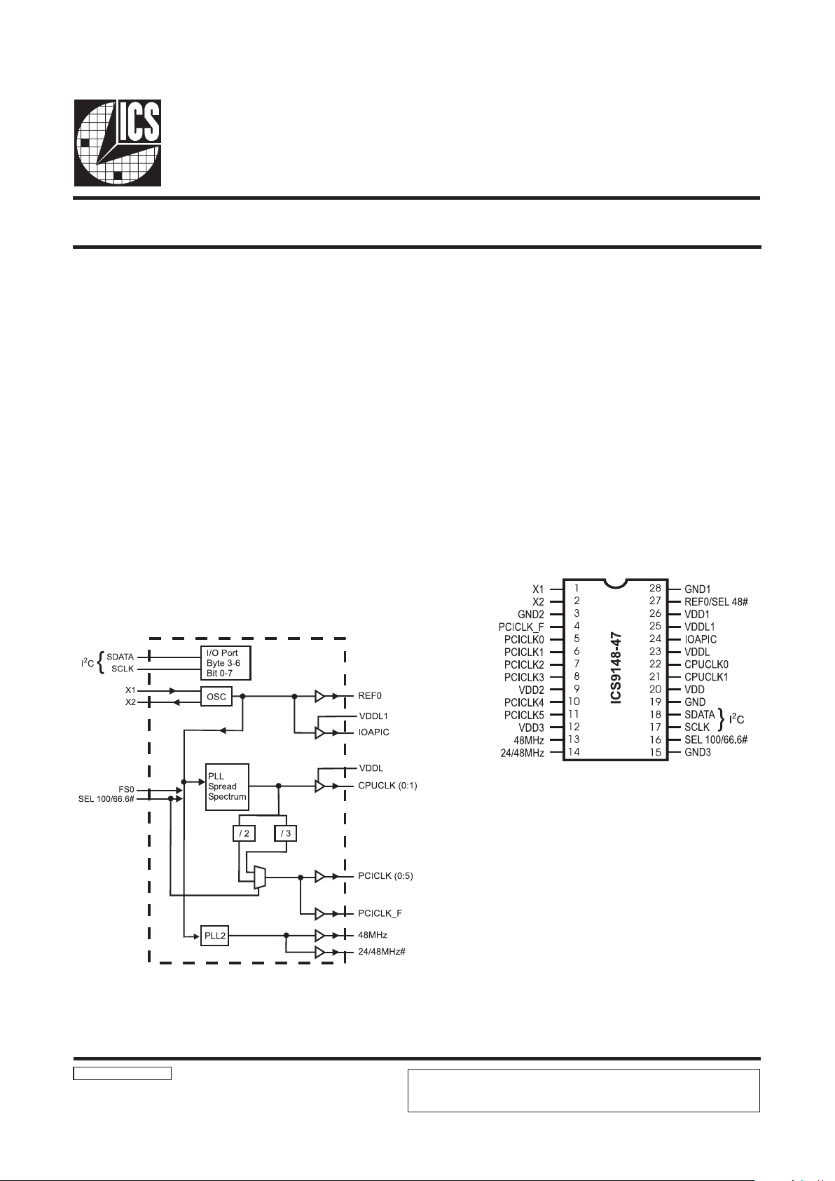
ICS9148-47
Block Diagram
Pentium/ProTM System Clock Chip
9148-47 Rev D 08/04/98
Pin Configuration
28 pin SOIC
Pentium is a trademark on Intel Corporation.
Generates system clocks for CPU, PCI, IOAPIC ,
14.314 MHz, 48 and 24MHz.
Supports single or dual processor systems
Skew from CPU (earlier) to PCI clock 1 to 4ns
Separate 2.5V and 3.3V supply pins
2.5V outputs: CPU, IOAPIC
3.3V outputs: PCI, REF
No power supply sequence requirements
28 pin SOIC
Spread Sectrum operation optional for PLL1
CPU frequencies to 100MHz are supported.
The ICS9148-47 is part of a reduced pin count two-chip clock
solution for designs using an Intel BX style chipset.
Companion SDRAM buffers are ICS9179-11 and 12.
There are two PLLs, with the first PLL capable of spread
spectrum operation. Spread spectrum typically reduces system
EMI by 8-10dB. The second PLL provides support for USB
(48MHz) and 24MHz requirements. CPU frequencies up to
100MHz are supported.
The I2C interface allows stop clock programming, frequency
selection, and spread spectrum operation to be programmed.
Clock outputs include two CPU (2.5V or 3.3V), seven PCI
(3.3V), one REF (3.3V), one IOAPIC (2.5V or 3.3V), one 48MHz,
and one selectable 48/24MHz.
Ground Groups
GND = Ground Source Core
GND1 = REF0, X1, X2
GND2 = PCICLK_F, PCICLK (0:5)
GND3=48MHz
GNDL = CPUCLK (0:1)
Power Groups
VDD = Supply for PLL core
VDD1 = REF0, X1, X2
VDD2 = PCICLK_F, PCICLK (0:5)
VDD3 = 48MHz
VDDL = CPUCLK (0:1)
VDDL1=IOAPIC
ICS reserves the right to make changes in the device data identified in this
publication without further notice. ICS advises its customers to obtain the latest
version of all device data to verify that any information being relied upon by the
customer is current and accurate.
2
ICS9148-47
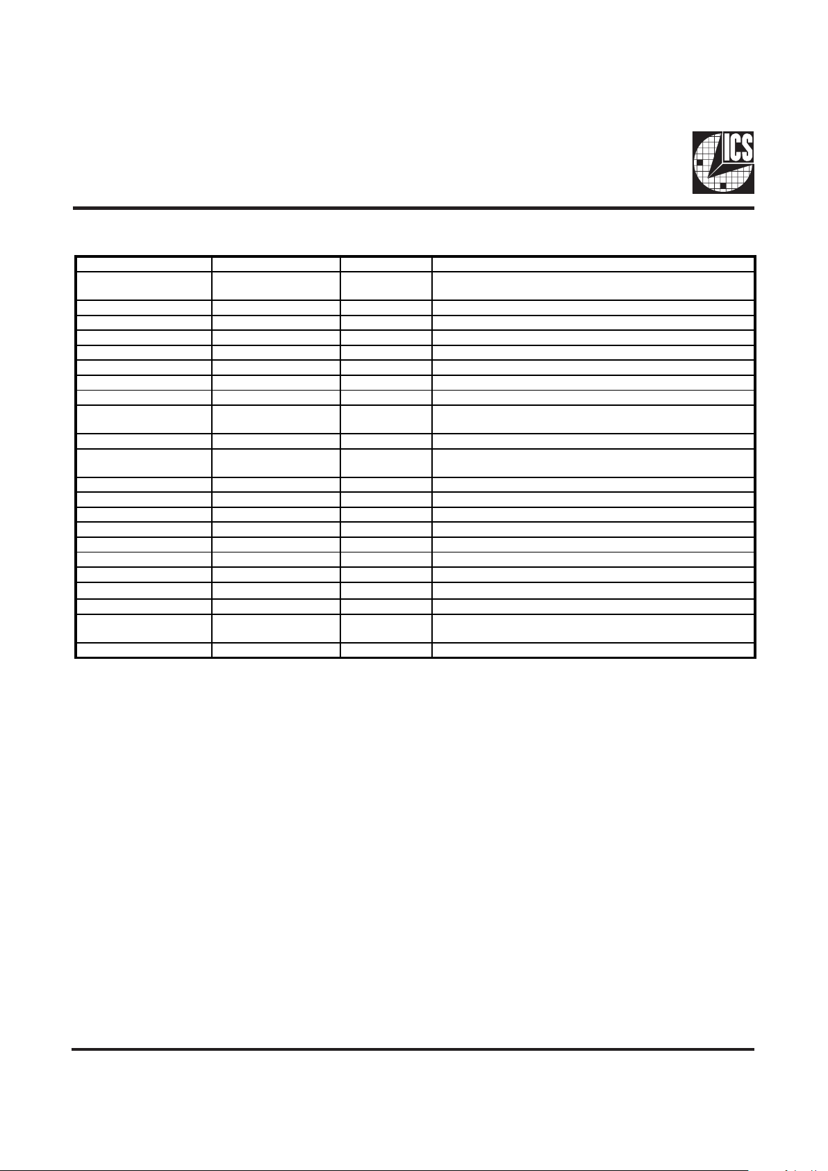
Pin Descriptions
PIN NUMBER PIN NAME TYPE DESCRIPTION
1X1IN
XTAL_IN 14.318MH z Crystal in put, has interna l 33pF load
cap and feed back resistor fro m X2
2 X2 OUT XTAL_OUT Crystal ou tput, has intern al load cap 33pF
3 GND2 PWR Ground for PCI outputs
4 PCICLK_F OUT Free Running PCI output
5, 6, 7, 8, 10 , 11 PCICLK (0:5) OUT PCI clock outp uts. TTL compati ble 3.3 V
6, 9 VDD2 PWR Power for PCICLK output s, nominally 3.3V
12 VDD3 PWR Poer for 48MHz
13 48MHz OUT Fixed CLK output @ 48MHz
14 24/48MHz OUT
Fixed CLK output; 24MHz if pin 27 =1 at power up, 48MHz
if pin 27=0 a t power up.
15 GND3 PWR Ground for 48MHz
16 SEL100/66 .6# IN
Select pin for enablin g 100MHz or 66.6M Hz
H=100MHz, L= 66.6MHz (PCI always synchronou s 33.3MHz)
17 SCLK IN Clock input for I
2
C input
18 SDATA IN Data input for I
2
C input
19 GND PWR Ground for CPUCL K (0:1 )
20 VDD PWR Power for PLL core
21, 22 CPUCLK (1:0) OUT CPU and Host clock outputs nominally 2.5V
23 VDDL PWR Power for CPU outputs, nominally 2.5V
24 IOAPIC OUT IOAPIC clock output 14.318MHz.
25 VDDL PWR Power for IOAPIC
26 VDD1 PWR Power for REF outputs.
27 REF0/SEL 48# OUT/IN
14.318MHz clock outpu t/Latched input at power up. When
low, pin 14 is 48MHz.
28 GND 1 PWR Ground for REF outputs, X1, X2.
3
ICS9148-47
General I2C serial interface information
The information in this section assumes familiarity with I2C programming. For more information, contact ICS for an I2C
programming application note.
How to Write:
Send the address D2
(H)
.
Send two additional dummy bytes, a command code
and byte count.
Send the desired number of data bytes.
See the diagram below:
Note that the acknowledge bit is sent by the clock chip, and pulls the data line low. There is no minimum of data bytes that must
be sent.
How to Read:
Send the address D3
(H)
.
Send the byte count in binary coded decimal
Read back the desired number of data bytes
See the diagram below:
The following specifications should be observed:
1. Operating voltage for I2C pins is 3.3V
2. Maximum data transfer rate (SCLK) is 100K bits/sec.
Clock Generator
Address (7 bits)
ACK
+ 8 bits
dummy
command code
ACK
+ 8 bits
dummy Byte
count
ACK
Data Byte
1
ACK
Data Byte
N
ACK
A(6:0) & R/W#
D2
(H)
Clock Generator
Address (7 bits)
ACK
Byte
Count
ACK
Data Byte
1
ACK
Data Byte
N
A(6:0) & R/W#
D3(H)

4
ICS9148-47
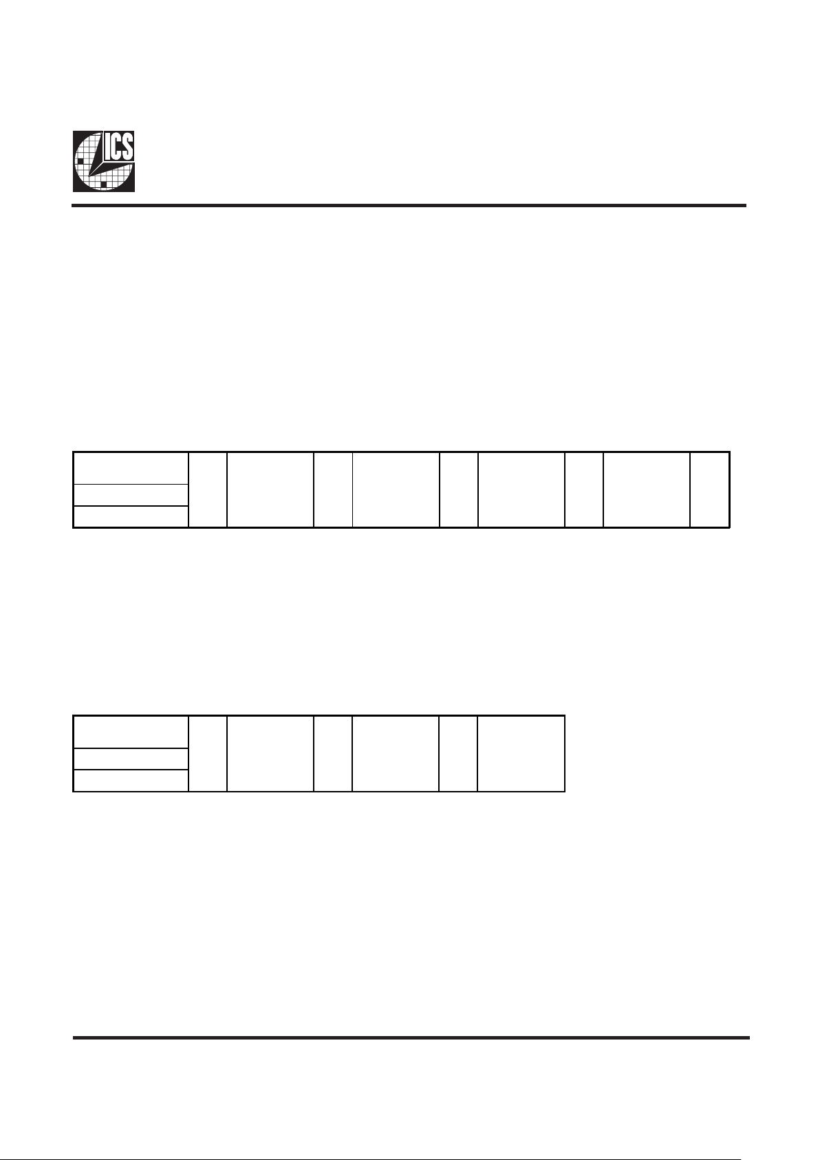
Note: PWD = Power-Up Default
Byte 3: Functionality & Frequency Select
& Spread Slect Register
Notes: 1 = Enabled; 0 = Disabled, outputs held low
Bit Description PWD
7(Reserved)0
6:4
Bit
654
CPU PCI
Spread
Percentage
000
001
010
011
100
101
110
111
68.5
75.0
83.3
66.6
103
112
133.3
100
34.25
37.5
41.6
33.3
34.3
37.3
44.43
33.33
±0.5% Center
±0.5% Center
±0.5% Center
±0.5% Center
±0.5% Center
±0.5% Center
±0.5% Center
±0.5% Center
0
3
0 - Frequency is selec ted by hard ware select
SEL100/66.6#
1 - Frequency is selected by 6:4 above
0
2(Reserved)
10
00 - Normal operation
01 - Test mode
10 - Spread sp rectrum ON
11 - Tristate all outputs
00
Byte 4:
Notes: 1 = Enabled; 0 = Disabled, outputs held low
Bit Pin# Pin Name PWD
Description
Bit Value = 0 Bit Value = 1
7 - - - (Reserved) (Reserved)
6 - - - (Reserved) (Reserved)
5 - - - (Reserved) (Reserved)
4 - - - (Reserved) (Reserved)
3 - - - (Reserved) (Reserved)
221CPUCLK11
Disabled
(low)
Enabled
1 - - 0 (Reserved) (Reserved)
022CPUCLK01
(Disabled)
(low)
Enabled
Byte 5:
Notes: 1 = Enabled; 0 = Disabled, outputs held low
Bit Pin# Pin Name PWD
Description
Bit Value = 0 Bit Value = 1
74PCICLK_F1
Disabled
(low)
Enabled
6 11 PCICLK5 1
Disabled
(low)
Enabled
5 10 PCICLK4 1
Disabled
(low)
Enabled
4 - - 0 (Reserved) (Reserved)
38PCICLK31
Disabled
(low)
Enabled
27PCICLK21
Disabled
(low)
Enabled
16PCICLK11
Disabled
(low)
Enabled
05PCICLK01
Disabled
(low)
Enabled
Serial Bitmap
Byte 6:
Notes:
1 = Enabled; 0 = Disabled, outputs held low
For pin 27, there are 2 output stages together for 1 pin. These 2
latches must be both 0 or 1 simultaneously or there will be a short to
ground if one is disabled and the other is running.
Bit Pin# Pin Name PWD
Description
Bit Value = 0 Bit Va lue = 1
7 - - 0 (Reserved) (Reserved)
6 - - 0 (Reserved) (Reserved)
524IOAPIC 1
Disabled
(low)
Enabled
4 - - 0 (Reserved) (Reserved)
3 - - 0 (Rese rved) (Reserved)
2 - - 0 (Reserved) (Reserved)
127 REF0 1
(Disabled)
(low)
Enabled
027 REF0 1
(Disabled)
(low)
Enabled

5
ICS9148-47
Absolute Maximum Ratings
Supply Voltage . . . . . . . . . . . . . . . . . . . . . . . . . . . 7.0 V
Logic Inputs . . . . . . . . . . . . . . . . . . . . . . . . . . . . GND 0.5 V to VDD +0.5 V
Ambient Operating Temperature . . . . . . . . . . . . 0°C to +70°C
Storage Temperature . . . . . . . . . . . . . . . . . . . . . . 65°C to +150°C
Stresses above those listed under Absolute Maximum Ratings may cause permanent damage to the device. These ratings are
stress specifications only and functional operation of the device at these or any other conditions above those listed in the
operational sections of the specifications is not implied. Exposure to absolute maximum rating conditions for extended periods
may affect product reliability.
Electrical Charact eristics - Input/Supply/Com m on O utput Parameters
TA = 0 - 70C; Supply Voltage VDD = V
DDL
= 3.3 V +/ -5% (unle s s otherwise s ta te d)
PARAMETER SYMBOL CONDITIONS MIN TYP MAX UNITS
Input High Voltage V
IH
2V
DD
+0.3 V
Input L ow Volta ge V
IL
VSS-0.3 0.8 V
Inpu t High Cur rent I
IH
VIN = V
DD
0.1 5
µ
A
Input Low Current I
IL1
VIN = 0 V; Input s w i t h no pul l -up resistor s -5 2.0
µ
A
Input Low Current I
IL2
VIN = 0 V; Input s w i t h pul l -up resistor s -200 -100
µ
A
Operating I
DD3.3OP66CL
= 0 pF; Select @ 66MHz 60 170 mA
Suppl y C urrent I
DD3.3OP100CL
= 0 pF; Select @ 100MHz 66 170
Power Down I
DD3.3PD
CL = 0 pF; With i nput addr ess to Vdd or GND 3 650
µ
A
Suppl y C urrent
Input frequen cy F
i
VDD = 3.3 V; 14.318 MH z
Input Capacita nce
1
C
IN
Logic Inputs 5 pF
C
INX
X 1 & X2 pins 27 36 45 pF
Tr a nsition Time
1
T
trans
To 1st cros sing of ta rget Freq. 3 ms
Settling Tim e
1
T
s
From 1st cr ossing to 1% t a rget Freq. 5 ms
Clk Stabiliza tion
1
T
STAB
From VDD = 3.3 V to 1% target Freq. 3 ms
Skew
1
T
AGP-PCI1VT
= 1.5 V;
13.54 ns
1
G ua ranteed by de sign, not 100% tes t ed in production.

6
ICS9148-47
Electrical Characteristics - Input /S upply/ Com m on O ut put Paramet ers
TA = 0 - 70C; Supply Voltage VDD = 3.3 V +/-5%, V
DDL
= 2.5 V + /- 5% (u nl e ss otherwise stated)
PARAMETER SYMBOL CONDITIONS MIN TY P MAX UNITS
Oper ating I
DD2.5OP66
CL = 0 pF; Select @ 66.8 MHz 16 72 mA
Supply Cu r r e nt I
DD2. 5OP100CL
= 0 pF; Select @ 100 MHz 23 100 m A
Power Down Supply
Current
I
DD2.5PD
CL = 0 pF; With input ad dr es s to Vdd
or G ND
10 100
µ
A
t
CPU-AGP
00.51 ns
t
CPU-PCI2
VT = 1.5 V; VTL = 1.25 V
12.64 ns
1
G uaranteed by design, not 100% tested in production.
Skew
1
Ele ctri ca l Characteristics - CPUCLK
TA = 0 - 70C; VDD = 3.3 V +/-5%, V
DDL
= 2.5 V +/ -5%; CL = 20 pF (unless otherwise stated)
PARAMETER SYMBO L CON D ITI ON S MIN TYP MAX UNI TS
Output High Voltage V
OH2B
IOH = -12.0 m A 2 2. 3 V
Output Low Voltage V
OL2B
IOL = 12 mA 0.2 0.4 V
O utput High Current I
OH2B
VOH = 1 .7 V - 41 -19 mA
Ou tput Low Current I
OL2B
VOL = 0.7 V 19 37 mA
Rise Time t
r2B
1
VOL = 0.4 V, VOH = 2.0 V 1.25 1.6 ns
Fall Time t
f2B
1
VOH = 2.0 V, VOL = 0 .4 V 1 1. 6 ns
Duty Cycle d
t2B
1
VT = 1.25 V 454855%
Skew t
sk2B
1
VT = 1.25 V 30 175 ps
Jitter, Cycle-to-cycle t
jcyc-cyc2B
1
VT = 1.25 V 150 250 ps
Jitter, One Sigm a t
j1s2B
1
VT = 1.25 V 40 150 ps
Jitter, Abs olute
t
jabs2B
1
VT = 1.25 V
-2 50 140 + 250 ps
1
G ua ranteed by d e sign, not 100% tes t ed in production.

7
ICS9148-47
Electrical Characteristics - PCICLK
TA = 0 - 70C; VDD = V
DDL
= 3.3 V +/-5%; CL = 30 pF
PARAMETER SY MBOL CONDITIONS MIN TYP MAX UNITS
O utput High Voltage V
OH1
IOH = -11 mA 2.4 3.1 V
Output Low Voltage V
OL1
IOL = 9.4 mA 0.1 0.4 V
Ou tput Hig h Current I
OH1
VOH = 2.0 V -62 -22 mA
Output Low Current I
OL1
VOL = 0.8 V 16 57 m A
Rise Time
1
t
r1
VOL = 0.4 V, VOH = 2.4 V 1.5 2 ns
Fall Time
1
t
f1
VOH = 2.4 V , VOL = 0.4 V 1.1 2 ns
Duty Cycle
1
d
t1
VT = 1.5 V 45 50 55 %
Skew
1
t
sk1
VT = 1.5 V 140 500 ps
Jitter, One S igm a
1
t
j1s1
VT = 1.5 V 17 150 ps
Jitter, Absolute
1
t
jabs1
VT = 1.5 V
-500 70 500 ps
1
Guar a nt eed by design, not 100% tested in product ion.
Electrical Characteristics - IOAPIC
TA = 0 - 70C; VDD = 3.3 V +/-5%, V
DDL
= 2.5 V +/-5%; CL = 20 pF
PARAMETER SY MBOL CONDITIONS MIN TYP MAX UNITS
O utput High Voltage V
OH4BIOH
= -18 mA 2 2.2 V
Output Low Voltage V
OL4B
IOL = 18 mA 0.33 0.4 V
Ou tput Hig h Current I
OH4B
VOH = 1.7 V -41 -28 mA
Output Low Current I
OL4B
VOL = 0.7 V 29 37 m A
Rise Time
1
T
r4B
VOL = 0.4 V, VOH = 2.0 V 1.3 1.6 ns
Fall Time
1
T
f4B
VOH = 2.0 V , VOL = 0.4 V 1.1 1.6 ns
Duty Cycle
1
D
t4B
VT = 1.25 V 45 54 55 %
Ske w
1
t
sk4B
1
VT = 1.25 V 60 250 ps
Jitter, One S igm a
1
T
j1s4B
VT = 1.25 V 1 3 %
Jitter, Absolute
1
T
jabs4B
VT = 1.25 V
-5 5 %
1
Guar a nt eed by design, not 100% tested in product ion.

8
ICS9148-47
Ele ctrical C haracteristics - 48, 24 MHz
TA = 0 - 70C; VDD = V
DDL
= 3.3 V +/-5%; CL = 20 pF (unless otherwise stat ed)
PARAMETER SY MBOL CONDITIONS MIN TY P MAX UNITS
O utput High Voltage V
OH5
IOH = -12 mA 2.6 3 V
Output Low Voltage V
OL5
IOL = 9 mA 0.14 0.4 V
Ou tput Hig h Current I
OH5
VOH = 2.0 V -44 -22 mA
Output Low Current I
OL5
VOL = 0.8 V 16 42 m A
Rise Time
1
t
r5
VOL = 0.4 V, VOH = 2.4 V 1.2 4 ns
Fall Time
1
t
f5
VOH = 2.4 V , VOL = 0.4 V 1.2 4 ns
Duty Cycle
1
d
t5
VT = 1.5 V 45 52 55 %
Jitter, One S igm a
1
t
j1s5
VT = 1.5 V 1 3 %
Jitter, Absolute
1
t
jabs5
VT = 1.5 V
35%
1
Guar a nt eed by design, not 100% tested in product ion.
Ele ctrical C haracteristics - REF
TA = 0 - 70C; VDD = V
DDL
= 3.3 V +/-5%; CL = 20 pF (unless otherwise stat ed)
PARAMETER SY MBOL CONDITIONS MIN TY P MAX UNITS
O utput High Voltage V
OH5
IOH = -12 mA 2.6 3.1 V
Output Low Voltage V
OL5
IOL = 9 mA 0.17 0.4 V
Ou tput Hig h Current I
OH5
VOH = 2.0 V -44 -22 mA
Output Low Current I
OL5
VOL = 0.8 V 29 42 m A
Rise Time
1
t
r5
VOL = 0.4 V, VOH = 2.4 V 1.4 2 ns
Fall Time
1
t
f5
VOH = 2.4 V , VOL = 0.4 V 1.1 2 ns
Duty Cycle
1
d
t5
VT = 1.5 V 47 54 57 %
Jitter, One S igm a
1
t
j1s5
VT = 1.5 V 1 3 %
Jitter, Absolute
1
t
jabs5
VT = 1.5 V
35%
1
Guar a nt eed by design, not 100% tested in product ion.

9
ICS9148-47
SOIC Package
LEAD COUNT 28L
DIMENSION L 0.704
Ordering Information
ICS9148M-47
Pattern Number (2 or 3 digit number for parts with ROM code patterns)
Package Type
M=SOIC
Device Type (consists of 3 or 4 digit numbers)
Prefix
ICS, AV = Standard Device
Example:
ICS XXXX M - PPP
ICS reserves the right to make changes in the device data identified in this
publication without further notice. ICS advises its customers to obtain the latest
version of all device data to verify that any information being relied upon by the
customer is current and accurate.
 Loading...