

Integrated
Circuit
Systems, Inc.
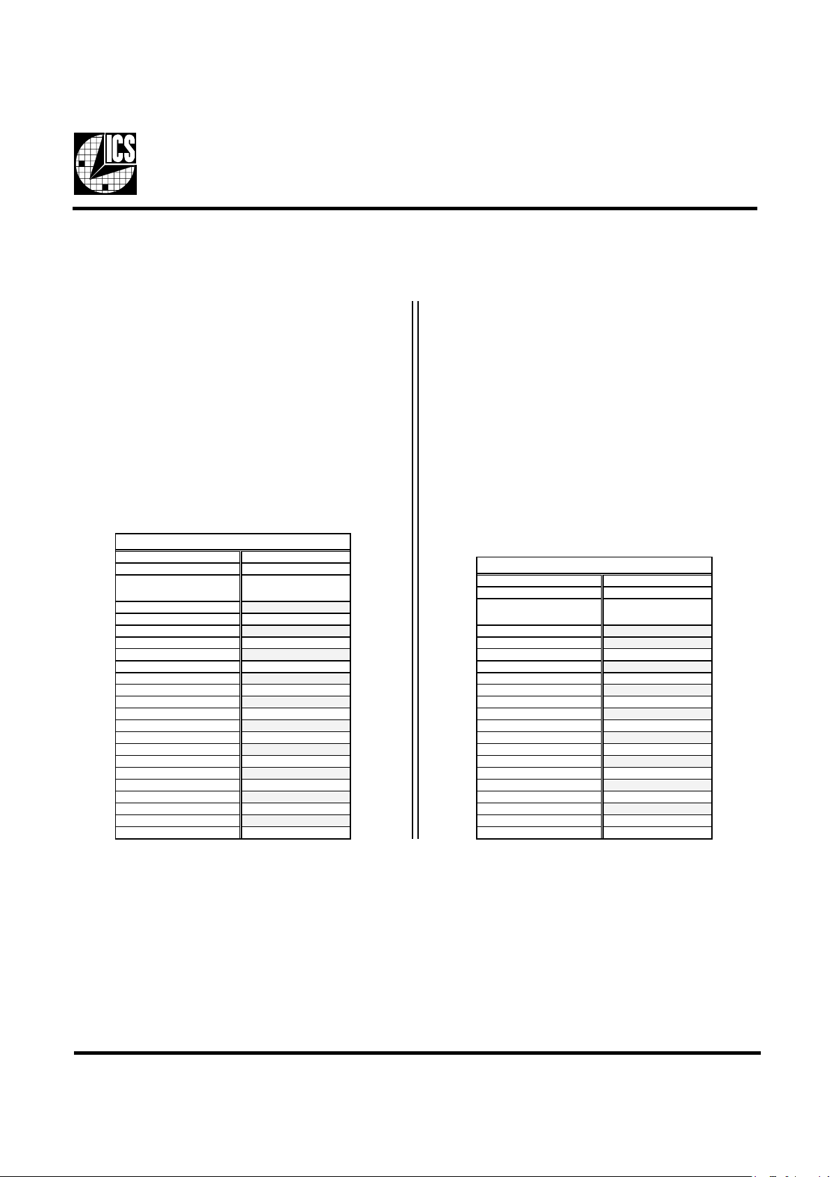
General Description Features
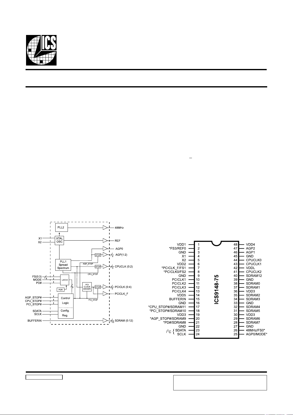
ICS9148-75
Block Diagram
Pentium is a trademark of Intel Corporation
I2C is a trademark of Philips Corporation
Frequency Generator & Integrated Buffers for Mother Boards
9148-75 Rev C 3/01/00
Pin Configuration
48-Pin SSOP
Power Groups
VDD1 = REF (0:1), X1, X2
VDD2 = PCICLK_F, PCICLK(0:5)
VDD3 = SDRAM (0:11), supply for PLL core
VDD4 = AGP (1:2)
VDD5 = Fixed PLL, 48MHz , AGP0
VDDL = CPUCLK (0:3)
* Internal Pull-up Resistor of
240K to 3.3V on indicated inputs
The ICS9148-75 generates all clocks required for high speed
RISC or CISC microprocessor systems such as Intel
PentiumPro™, AMD™ or Cyrix™. Sixteen different reference
frequency multiplying factors are externally selectable with
smooth frequency transitions.
Spread spectrum may be enabled through I2C programming.
Spread spectrum typically reduces system EMI by 8dB to
10dB. This simplifies EMI qualification without resorting to
board design iterations or costly shielding. The ICS9148-75
employs a proprietary closed loop design, which tightly
controls the percentage of spreading over process and
temperature variations.
Serial programming I2C interface allows changing functions,
stop clock programming and frequency selection. The
SDRAM12 output may be used as a feed back into an off chip
PLL.
• Generates the following system clocks:
- 3 CPU(2.5V/3.3V) up to 100MHz.
- 6 PCI(3.3V) @ 33.3MHz (including one free
running PCICLK)
- 3AGP(3.3V) @ 2 x PCI
- 13 SDRAMs(3.3V) up to 100MHz
- 1 REF (3.3V) @ 14.318MHz
- 1 - 48MHz (3.3V) fixed
• Skew characteristics:
- CPU – CPU
<250ps
- CPU(early) – PCI : 1-4ns
- AGP – PCI: 250ps
- PCI – PCI <500ps
• Supports Spread Spectrum modulation & I2C
programming for Power Management, Frequency Select
• Efficient Power management scheme through power
down PCI, AGP and CPU_STOP clocks.
• Uses external 14.318MHz crystal
• 48 pin 300mil SSOP.
PRODUCT PREVIEW documents contain information on new
products in the sampling or preproduction phase of development.
Characteristic data and other specifications are subject to change
without notice.
Preliminary Product Preview
2
ICS9148-75
Preliminary Product Preview
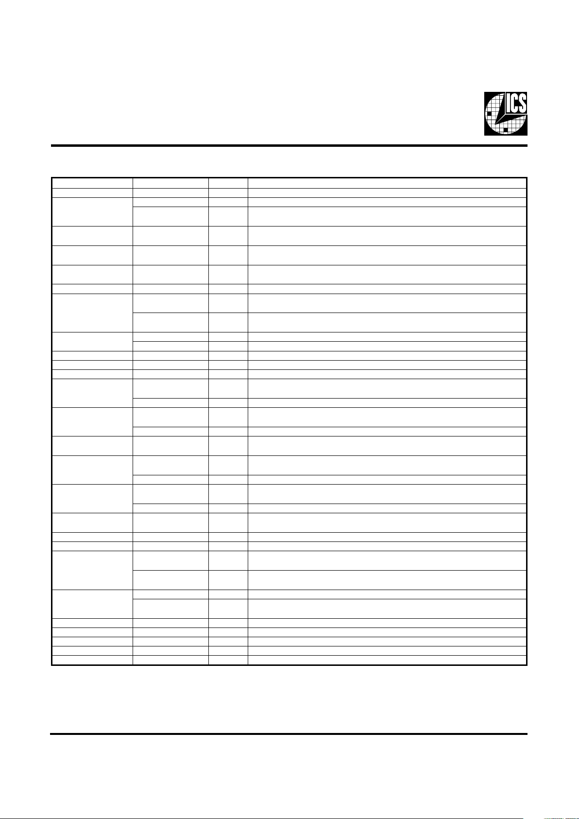
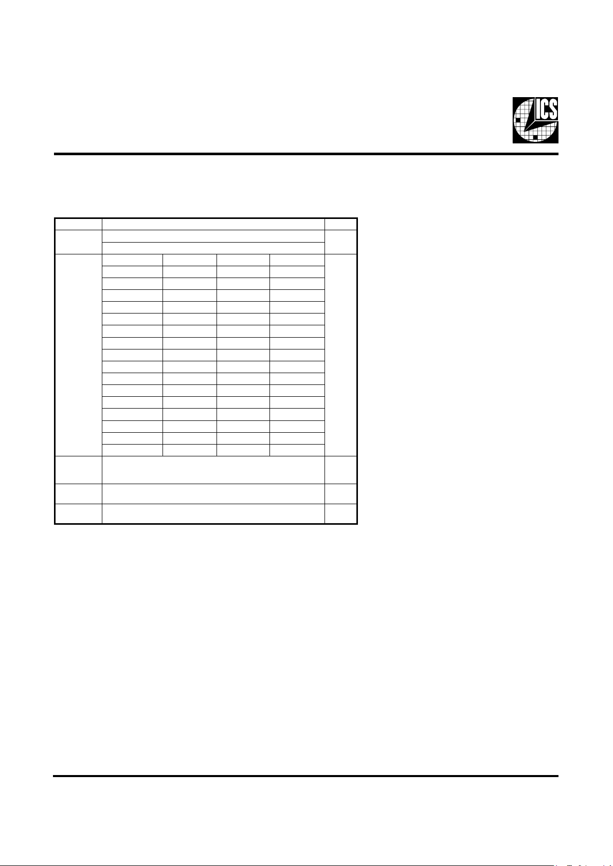
Pin Descriptions
Notes:
1: Internal Pull-up Resistor of 240K to 3.3V on indicated inputs
2: Bidirectional input/output pins, input logic levels are latched at internal power-on-reset. Use 10Kohm resistor to
program logic Hi to VDD or GND for logic low.
REBMUNNIPEMANNIPEPYTNOITPIRCSED
11DDVRWPV3.3lanimon,ylppusrewopLATX,)2:0(feR
2
0FERTUO.kcolcecnereferzHM813.41
3SFNI
ehtsnimretedsnipSFrehtohtiwgnolA.tupnIdehctaL.niptcelesycneuqerF
.seicneuwerfPGA&ICP,MARDS,UPC
,72,22,61,9,3
54,93,33
DNGRWPdnuorG
41XNI
kcabdeefdna)Fp33(pacdaollanretnisah,tupnilatsyrC
2Xmorfrotsiser
52XTUO
daollanretnisaH.zHM813.41yllanimon,tuptuolatsyrC
)Fp33(pac
62DDVRWPV3.3lanimon,)5:0(KLCICPdnaF_KLCICProfylppuS
7
F_KLCICPTUO
wekssn4-1htiwsKLCUPChtiwsuonorhcnyS.tuptuokcolcICPgninnureerF
#POTS_ICPybdetceffatonsisihT)ylraeUPC(
1SF
2,1
NI
ehtsnimretedsnipSFrehtohtiwgnolA.tupnIdehctaL.niptcelesycneuqerF
.seicneuwerfPGA&ICP,MARDS,UPC
8
0KLCICPTUO )ylraeUPC(wekssn4-1htiwsKLCUPCsuonuorhcnyS.stuptuokcolcICP
2SF
2,1
NItupnIdehctaL.niptcelesycneuqerF
31,21,11,01)4:1(KLCICPTUO )ylraeUPC(wekssn4-1htiwsKLCUPCsuonuorhcnyS.stuptuokcolcICP
415DDVRWP0PGA,zHM84,LLPdexifrofylppuS
51NIREFFUBNI.sreffubMARDSrofniptupnI
71
#POTS_UPCNI
eliboMni(woltupninehw,level0cigoltaskcolc)3:0(KLCUPCstlaH
)0=EDOM,edoM
11MARDSTUOtuptuokcolcMARDS
81
#POTS_ICP
1
NI
,edomelibomnI(woltupninehw,level0cigoltaskcolc)5:0(KLCICPstlaH
)0=EDOM
01MARDSTUOtuptuokcolcMARDS
,43,23,13,92,82
83,73,53
)9:0(MARDSTUO.stuptuokcolcMARDS
02
#POTS_PGA
1
NI
tupninehwlevel"0"cigoltaskcolc)2:1(PGAstlahtupnisuonorhcnysasihT
0PGAtceffatonseoD)0=EDOM,edoMeliboMni(wol
9MARDSTUOtuptuokcolcMARDS
12
#DP
1
NI
lanretni&latsyrc,OCVehtspotStupninwoDrewoPsuonorehcnysasihT
)0=EDOM,edoMeliboMnI(.woL,evitcanehwskcolc
8MARDSTUOtuptuokcolcMARDS
63,03,913DDVRWP
,skcolczHM84,eroCUPC,)11:0(MARDSrofylppuS
.V3.3lanimon
32ATADSNIIroftupniataD
2
.tupnilairesC
42KLCSNIIfotupnikcolC
2
tupniC
52
0PGATUO
ybdetceffatoN.4DDVybderewop,tuptuotroPcihparGdecnavdA
#POTS_PGA
EDOM
2,1
NI
.edoMeliboM=0,edoMpotkseD=1,niptcelesnoitcnuf12&02,81,71niP
.tupnIdehctaL
62
zHM84TUO.gnimitBSUrofkcolctuptuozHM84
0SF
2,1
NI
ehtsnimretedsnipSFrehtohtiwgnolA.tupnIdehctaL.niptcelesycneuqerF
.seicneuwerfPGA&ICP,MARDS,UPC
44,34,14)3:0(KLCUPCTUOwoL=#POTS_UPCfiwoL.2LDDVybderewop,stuptuokcolcUPC
0421MARDSTUO.tuptuokcolcMARDSkcabdeeF
24LDDVRWPlanimonV3.3roV5.2rehtie,)3:0(UPCrofylppuS
74,64)2:1(PGATUO.4DDVybderewoptuptuotroPcihparGdecnavdA
844DDVRWP)2:0(PGArofylppuS
3
ICS9148-75
Preliminary Product Preview
5.2_#3.3UPC
leveltupnI
)ataDdehctaL(
rofdetceleSreffuB
:tanoitarepo
1DDVV5.2
0DDVV3.3
CPU 3.3#_2.5V Buffer selector for CPUCLK drivers.
Power Management Functionality
Mode Pin - Power Management Input Control
52niP,EDOM
)tupnIdehctaL(
71niP81niP02niP12niP
0
#POTS_UPC
)TUPNI(
#POTS_ICP
)TUPNI(
#POTS_PGA
)TUPNI(
#DP
)TUPNI(
1
11MARDS
)TUPTUO(
01MARDS
)TUPTUO(
9MARDS
)TUPTUO(
8MARDS
)TUPTUO(
#POTS_PGA#POTS_UPC#POTS_ICP
KLCUPC
stuptuO
KLCICP
)5:0(
,F_KLCICP
zHM84,FER
MARDSdna
latsyrC
CSO
OCV)2:1(PGA
101 woLdeppotSgninnuRgninnuRgninnuRgninnuRgninnuR
111 gninnuRgninnuRgninnuRgninnuRgninnuRgninnuR
110 gninnuRwoLdeppotSgninnuRgninnuRgninnuRgninnuR
011 gninnuRgninnuRgninnuRgninnuRgninnuRwoLdeppotS
4
ICS9148-75
Preliminary Product Preview
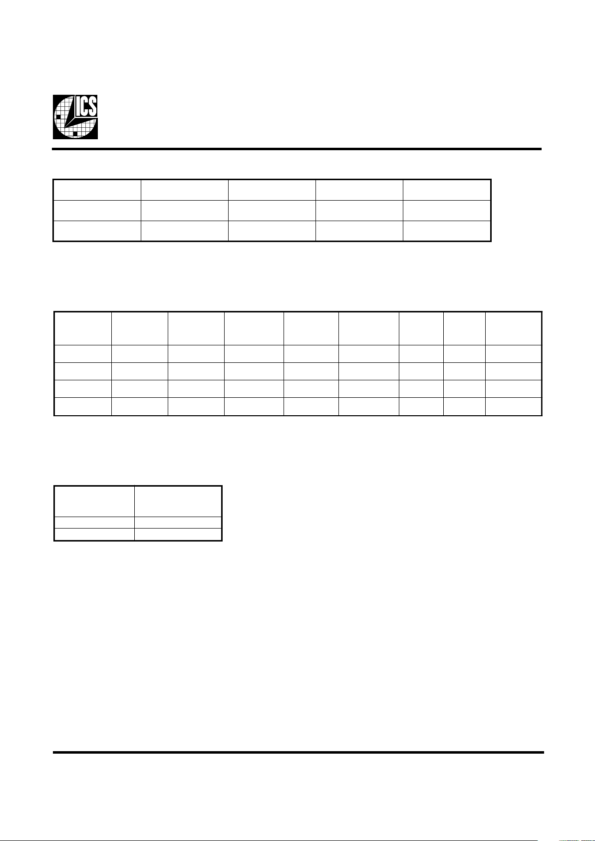
Functionality
VDD1, 2, 3, 4 = 3.3V±5%, TA= 0 to 70°C
Crystal (X1, X2) = 14.31818MHz
FS3 FS2 FS1 FS0
CPU, SDRAM
(MHZ) PCI (MHZ) AGP (MHZ)
REF, IOAPIC
(MHZ)
1111 105 35 7014.318
1110 110 36.6773.3414.318
1101 115 38.3376.6614.318
1100 120 40 8014.318
1011 125 41.6683.3214.318
1010 130 43.3386.6614.318
1001 135 45 9014.318
1000 140 46.6793.4414.318
0111 100 33.366.614.318
0110 95.25 31.7563.514.318
0101 83.3 33.366.614.318
0100 75 30 6014.318
0011 75 37.57514.318
0010 68.5 34.2568.514.318
0001 66.8 33.466.814.318
0000
60 30 60 14.318
5
ICS9148-75
Preliminary Product Preview
1. The ICS clock generator is a slave/receiver, I2C component. It can read back the data stored in the latches for verification.
Read-Back will support Intel PIIX4 "Block-Read" protocol.
2. The data transfer rate supported by this clock generator is 100K bits/sec or less (standard mode)
3. The input is operating at 3.3V logic levels.
4. The data byte format is 8 bit bytes.
5. To simplify the clock generator I2C interface, the protocol is set to use only "Block-Writes" from the controller. The
bytes must be accessed in sequential order from lowest to highest byte with the ability to stop after any complete byte
has been transferred. The Command code and Byte count shown above must be sent, but the data is ignored for those
two bytes. The data is loaded until a Stop sequence is issued.
6. At power-on, all registers are set to a default condition, as shown.
General I2C serial interface information
The information in this section assumes familiarity with I2C programming.
For more information, contact ICS for an I2C programming application note.
How to Write:
• Controller (host) sends a start bit.
• Controller (host) sends the write address D2
(H)
• ICS clock will acknowledge
• Controller (host) sends a dummy command code
• ICS clock will acknowledge
• Controller (host) sends a dummy byte count
• ICS clock will acknowledge
• Controller (host) starts sending first byte (Byte 0)
through byte 5
• ICS clock will acknowledge each byte one at a time.
• Controller (host) sends a Stop bit
How to Read:
• Controller (host) will send start bit.
• Controller (host) sends the read address D3
(H)
• ICS clock will acknowledge
• ICS clock will send the byte count
• Controller (host) acknowledges
• ICS clock sends first byte (Byte 0) through byte 6
• Controller (host) will need to acknowledge each byte
• Controller (host) will send a stop bit
Notes:
Controller (Host) ICS (Slave/Receiver)
Start Bit
Address
D2
(H)
A
CK
Dummy Command Code
A
CK
Dummy Byte Count
ACK
Byte 0
A
CK
Byte 1
A
CK
Byte 2
ACK
Byte 3
A
CK
Byte 4
A
CK
Byte 5
ACK
Byte 6
A
CK
Stop Bit
How to Write:
Controller (Host) ICS (Slave/Receiver)
Start Bit
Address
D3
(H)
A
CK
Byte Count
ACK
Byte 0
ACK
Byte 1
ACK
Byte 2
ACK
Byte 3
ACK
Byte 4
ACK
Byte 5
ACK
Byte 6
ACK
Stop Bit
How to Read:
6
ICS9148-75
Preliminary Product Preview
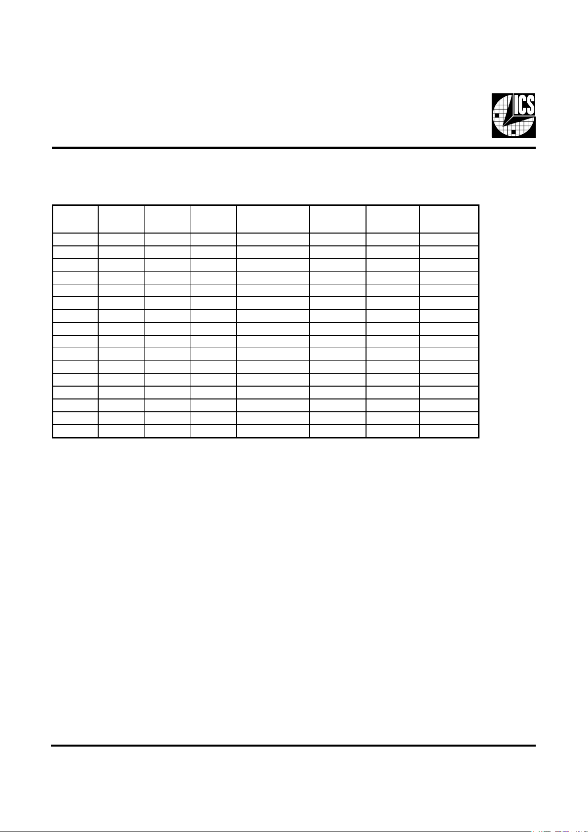
Byte0: Functionality and Frequency Select Register (default = 0)
Serial Configuration Command Bitmap
I2C is a trademark of Philips Corporation
Note 1: Default at power-up will be for latched logic inputs to define frequency;
Bits 2, 6:4 are default to 000
Note: PWD = Power-Up Default
tiBnoitpircseDDWP
7tiB
noitaludoMmurtcepSdaerpS%52.0±-0
0
noitaludoMmurtcepSdaerpS%6.0±-1
tiB
)4:6,2(
)4:6,2(tiBsKLCUPCsKLCICPsKLCPGA
1etoN
11115015307
011101176.6343.37
101151133.8366.67
00110210408
110152166.1423.38
010103133.3466.68
10015315409
000104176.6444.39
11100013.336.66
011052.5957.135.36
10103.383.336.66
0010570306
1100575.7357
01005.8652.435.86
10008.664.338.66
0000060306
3tiB
,tceleserawdrahybdetcelessiycneuqerF-0
stupnIdehctaL
)evoba(4:6tiBybdetcelessiycneuqerF-1
0
1tiB
lamroN-0
)daerpsretnec(delbanEmurtcepSdaerpS-1
0
0tiB
gninnuR-0
stuptuollaetatsirT-1
0

7
ICS9148-75
Preliminary Product Preview
Byte 1: CPU, Active/Inactive Register
(1 = enable, 0 = disable)
Byte 3: SDRAM Active/Inactive Register
(1 = enable, 0 = disable)
Notes:
1. Inactive means outputs are held LOW and are disabled
from switching.
Notes:
1. Inactive means outputs are held LOW and are disabled
from switching.
Notes:
1. Inactive means outputs are held LOW and are disabled
from switching.
tiB#niPDWPnoitpircseD
7tiB-1 )devreseR(
6tiB-1 )devreseR(
5tiB-1 )devreseR(
4tiB-1 )devreseR(
3tiB041 )tcanI/tcA(3KLCUPC
2tiB141 )tcanI/tcA(2KLCUPC
1tiB341 )tcanI/tcA(1KLCUPC
0tiB441 )tcanI/tcA(0KLCUPC
tiB#niPDWPnoitpircseD
7tiB-1 )devreseR(
6tiB71 )tcanI/tcA(F_KLCICP
5tiB511 )tcanI/tcA(5KLCICP
4tiB311 )tcanI/tcA(4KLCICP
3tiB211 )tcanI/tcA(3KLCICP
2tiB111 )tcanI/tcA(2KLCICP
1tiB011 )tcanI/tcA(1KLCICP
0tiB81 )tcanI/tcA(0KLCICP
tiB#niPDWPnoitpircseD
7tiB821 )tcanI/tcA(7MARDS
6tiB921 )tcanI/tcA(6MARDS
5tiB131 )tcanI/tcA(5MARDS
4tiB231 )tcanI/tcA(4MARDS
3tiB431 )tcanI/tcA(3MARDS
2tiB531 )tcanI/tcA(2MARDS
1tiB731 )tcanI/tcA(1MARDS
0tiB831 )tcanI/tcA(0MARDS
Byte 4: SDRAM Active/Inactive Register
(1 = enable, 0 = disable)
Byte 5: Peripheral Active/Inactive Register
(1 = enable, 0 = disable)
Notes:
1. Inactive means outputs are held LOW and are disabled
from switching.
Notes:
1. Inactive means outputs are held LOW and are disabled
from switching.
tiB#niPDWPnoitpircseD
7tiB521 )evitcanI/evitcA(0PGA
6tiB-1 )devreseR(
5tiB62-#0SF
4tiB-1 )devreseR(
3tiB711
)tcanI/tcA(11MARDS
)ylnOedoMpotkseD(
2tiB811
)tcanI/tcA(01MARDS
)ylnOedoMpotkseD(
1tiB021 )tcanI/tcA(9MARDS
0tiB121 )tcanI/tcA(8MARDS
tiB#niPDWPnoitpircseD
7tiB-1 )devreseR(
6tiB8-#2SF
5tiB7-#1SF
4tiB741 )tcanI/tcA(2PGA
3tiB-1 )devreseR(
2tiB2-#3SF
1tiB641 )tcanI/tcA(1PGA
0tiB21 )tcanI/tcA(0FER
Byte 2: PCI Active/Inactive Register
(1 = enable, 0 = disable)
Byte 6: Optional Register for Possible
Future Requirements
Notes:
1. Byte 6 is reserved by Integrated Circuit Systems for
future applications.
tiB#niPDWPnoitpircseD
7tiB-1 )devreseR(
6tiB-1 )devreseR(
5tiB-1 )devreseR(
4tiB-1 )devreseR(
3tiB-1 )devreseR(
2tiB-1 )devreseR(
1tiB-1 )devreseR(
0tiB-1 )devreseR(

8
ICS9148-75
Preliminary Product Preview
CPU_STOP# Timing Diagram
CPU_STOP# is an asychronous input to the clock synthesizer. It is used to turn off the CPU clocks for low power operation.
CPU_STOP# is synchronized by the ICS9148-75. The minimum that the CPU clock is enabled (CPU_STOP# high pulse) is 100
CPU clocks. All other clocks will continue to run while the CPU clocks are disabled. The CPU clocks will always be stopped in
a low state and start in such a manner that guarantees the high pulse width is a full pulse. CPU clock on latency is less than 4
CPU clocks and CPU clock off latency is less than 4 CPU clocks.
Notes:
1. All timing is referenced to the internal CPU clock.
2. CPU_STOP# is an asynchronous input and metastable conditions may exist. This signal is synchronized
to the CPU clocks inside the ICS9148-75.
3. All other clocks continue to run undisturbed. (including SDRAM outputs).

9
ICS9148-75
Preliminary Product Preview
PCI_STOP# Timing Diagram
PCI_STOP# is an asynchronous input to the ICS9148-75. It is used to turn off the PCICLK (0:5) clocks for low power operation.
PCI_STOP# is synchronized by the ICS9148-75 internally. The minimum that the PCICLK (0:5) clocks are enabled (PCI_STOP#
high pulse) is at least 10 PCICLK (0:5) clocks. PCICLK (0:5) clocks are stopped in a low state and started with a full high pulse
width guaranteed. PCICLK (0:5) clock on latency cycles are only one rising PCICLK clock off latency is one PCICLK clock.
Notes:
1. All timing is referenced to the Internal CPUCLK (defined as inside the ICS9148 device.)
2. PCI_STOP# is an asynchronous input, and metastable conditions may exist. This signal is required to be synchronized
inside the ICS9148.
3. All other clocks continue to run undisturbed.
4. CPU_STOP# is shown in a high (true) state.

10
ICS9148-75
Preliminary Product Preview
AGP_STOP# Timing Diagram
AGP_STOP# is an asychronous input to the clock synthesizer. It is used to turn off the AGP (0:1) clocks. for low power
operation. AGP_STOP# is synchronized by the ICS9148-75. The AGP2 clock is free-running and is not affected by AGP_STOP#.
All other clocks will continue to run while the AGPCLKs are disabled. The AGPCLKs will always be stopped in a low state and
start in such a manner that guarantees the high pulse width is a full pulse. AGPCLK on latency is less than AGPCLK and
AGPCLK off latency is less than 4 AGPCLKs. This function is available only with MODE pin latched low.
Notes:
1. All timing is referenced to the internal CPUCLK.
2. AGP_STOP# is an asynchronous input and metastable conditions may exist.
This signal is synchronized to the CPUCLKs inside the ICS9148-75.
3. All other clocks continue to run undisturbed.
4. PD# and PCI_STOP# are shown in a high (true) state.
5. Only applies if MODE pin latched 0 at power up.

11
ICS9148-75
Preliminary Product Preview
Fig. 1
Shared Pin Operation Input/Output Pins
The I/O pins designated by (input/output) on the ICS9148-75
serve as dual signal functions to the device. During initial
power-up, they act as input pins. The logic level (voltage)
that is present on these pins at this time is read and stored
into a 5-bit internal data latch. At the end of Power-On reset,
(see AC characteristics for timing values), the device changes
the mode of operations for these pins to an output function.
In this mode the pins produce the specified buffered clocks
to external loads.
To program (load) the internal configuration register for these
pins, a resistor is connected to either the VDD (logic 1) power
supply or the GND (logic 0) voltage potential. A 10 Kilohm
(10K) resistor is used to provide both the solid CMOS
programming voltage needed during the power-up
programming period and to provide an insignificant load on
the output clock during the subsequent operating period.
Via to
VDD
Clock trace to load
Series Term. Res.
Programming
Header
Via to Gnd
Device
Pad
2K W
8.2K W
Figure 1 shows a means of implementing this function when
a switch or 2 pin header is used. With no jumper is installed
the pin will be pulled high. With the jumper in place the pin
will be pulled low. If programmability is not necessary, than
only a single resistor is necessary. The programming resistors
should be located close to the series termination resistor to
minimize the current loop area. It is more important to locate
the series termination resistor close to the driver than the
programming resistor.

12
ICS9148-75
Preliminary Product Preview
Absolute Maximum Ratings
Supply Voltage . . . . . . . . . . . . . . . . . . . . . . . . . . . 7.0 V
Logic Inputs . . . . . . . . . . . . . . . . . . . . . . . . . . . . GND –0.5 V to V
DD
+0.5 V
Ambient Operating Temperature . . . . . . . . . . . . 0°C to +70°C
Storage Temperature . . . . . . . . . . . . . . . . . . . . . . –65°C to +150°C
Stresses above those listed under Absolute Maximum Ratings may cause permanent damage to the device. These ratings are
stress specifications only and functional operation of the device at these or any other conditions above those listed in the
operational sections of the specifications is not implied. Exposure to absolute maximum rating conditions for extended periods
may affect product reliability.
Electrical Characteristics - Input/Supply/Common Output Parameters
TA = 0 - 70C; Supply Voltage VDD = V
DDL
= 3.3 V +/-5% (unless otherwise stated)
PARAMETER SYMBOL CONDITIONS MIN TYP MAX UNITS
Input High Voltage V
IH
2V
DD
+0.3 V
Inpu t Low Voltage V
IL
VSS-0.3 0.8 V
Input High Current I
IH
VIN = V
DD
0.15mA
Input Low Current I
IL1
VIN = 0 V; Inputs with no pull-up resistors -5 2.0 mA
Input Low Current I
IL2
VIN = 0 V; Inputs with pull-up resistors -200 -100 mA
Operating I
DD3.3OPCL
= 0 pF; 66.8 MHz 100 160 mA
Supply Current
Input frequency F
i
VDD = 3.3 V; 14.318 MHz
Input Capacitance
1
C
IN
Logic Inputs 5 pF
C
INX
X1 & X2 pins 27 36 45 pF
Transition Time
1
T
trans
To 1st crossing of target Freq. 2 ms
Settling Time
1
T
s
From 1st crossing to 1% target Freq. ms
Clk Stabilization
1
T
STAB
From VDD = 3.3 V to 1% target Freq. 2 ms
Skew
1
T
CPU-SDRAM1VT
= 1.5 V; SDRAM Leads -500 200 500 ps
T
CPU-PCI1VT
= 1.5 V; CPU Leads
256ns
1
Guaranteed by design, not 100% tested in production.
Electrical Characteristics - Input/Supply/Common Output Parameters
TA = 0 - 70C; Supply Voltage VDD = 3.3 V +/-5%, V
DDL
= 2.5 V +/-5% (unless otherwise stated)
PARAMETER SYMBOL CONDITIONS MIN TYP MAX UNITS
Operating I
DD2.5OP
CL = 0 pF; 66.8 MHz 10 20 mA
Supply Current
T
CPU-SDRAM2VT
= 1.5 V; VTL = 1.25 V; SDRAM Leads -500 200 500 ps
T
CPU-PCI2VT
= 1.5 V; VTL = 1.25 V; CPU Leads
256ns
1
Guaranteed by design, not 100% tested in production.
Skew
1

13
ICS9148-75
Preliminary Product Preview
Electrical Characteristics - CPU
TA = 0 - 70C; VDD = V
DDL
= 3.3 V +/-10%; CL = 10 - 20 pF (unless otherwise stated)
PARAMETER SYMBOL CONDITIONS MIN TYP MAX UNITS
Output High Voltage V
OH2AIOH
= -28 mA 2.5 2.6 V
Output Low Voltag e V
OL2AIOL
= 27 mA 0.35 0.4 V
Output High Current I
OH2 A
VOH = 2.0 V -29 -23 mA
Output Low Current I
OL2 A
VOL = 0.8 V 33 37 mA
Rise Time t
r2A
1
VOL = 0.4 V, VOH = 2.4 V 1.75 2 ns
Fall Time t
f2A
1
VOH = 2.4 V, VOL = 0.4 V 1.1 2 ns
Duty Cycle d
t2A
1
VT = 1.5 V 45 50 55 %
Skew t
sk2A
1
VT = 1.5 V 50 250 ps
Jitter, One Sigma t
j1s2A
1
VT = 1.5 V 65 150 ps
Jitter, Absolute
t
jabs2A
1
VT = 1.5 V
-250 165 250 ps
1
Guaranteed by design, not 100% tested in production.
Electrical Characteristics - PCI
TA = 0 - 70C; VDD = V
DDL
= 3.3 V +/-10%; CL = 30 pF (unless otherwise stated)
PARAMETER SYMBOL CONDITIONS MIN TYP MAX UNITS
Output High Voltage V
OH1IOH
= -28 mA 2.4 3 V
Output Low Voltag e V
OL1IOL
= 23 mA 0.2 0.4 V
Output High Current I
OH1
VOH = 2.0 V -60 -40 mA
Output Low Current I
OL1
VOL = 0.8 V 41 50 mA
Rise Time t
r1
1
VOL = 0.4 V, VOH = 2.4 V 1.8 2 ns
Fall Time t
f1
1
VOH = 2.4 V, VOL = 0.4 V 1.6 2 ns
Duty Cycle d
t1
1
VT = 1.5 V 45 50 55 %
Skew t
sk1
1
VT = 1.5 V 130 250 ps
Jitter, One Sigma
1
t
j1s1a
VT = 1.5 V, synchronous 40 150 ps
t
j1s1b
VT = 1.5 V, asynchronous 200 250 ps
Jitter, Absolute
1
tab
s1aVT
= 1.5 V, synchronous -250 135 250 ps
t
jabs1b
VT = 1.5 V, asynchronous
-650 500 650 ps
1
Guaranteed by design, not 100% tested in production.

14
ICS9148-75
Preliminary Product Preview
Electrical Characteristics - SDRAM
TA = 0 - 70C; VDD = V
DDL
= 3.3 V +/-5%; CL = 30 pF
PARAMETER SYMBOL CONDITIONS MIN TYP MAX UNITS
Output High Voltage V
OH1IOH
= -28 mA 2.4 3 V
Output Low Voltag e V
OL1
IOL = 23 mA 0.2 0.4 V
Output High Current I
OH1
VOH = 2.0 V -60 -40 mA
Output Low Current I
OL1
VOL = 0.8 V 41 50 mA
Rise Time
1
T
r1
VOL = 0.4 V, VOH = 2.4 V 1.75 2 ns
Fall Time
1
T
f1
VOH = 2.4 V, VOL = 0.4 V 1.5 2 ns
Duty Cycle
1
D
t1
VT = 1.5 V 45 50 55 %
Skew
1
T
sk1
VT = 1.5 V 200 500 ps
Jitter, One Sigma
1
T
j1s1
VT = 1.5 V 50 150 ps
Jitter, Absolute
1
T
jabs1
VT = 1.5 V (with synchronous PCI) -250 +250 ps
Jitter, Absolute
1
T
jabs1
VT = 1.5 V (with asynchronous PCI)
-400 400 ps
1
Guaranteed by design, not 100% tested in production.
Electrical Characteristics - AGP
TA = 0 - 70C; VDD = V
DDL
= 3.3 V +/-10%; CL = 30 pF (unless otherwise stated)
PARAMETER SYMBOL CONDITIONS MIN TYP MAX UNITS
Output High Voltage V
OH1IOH
= -28 mA 2.4 3 V
Output Low Voltag e V
OL1IOL
= 23 mA 0.2 0.4 V
Output High Current I
OH1
VOH = 2.0 V -60 -40 mA
Output Low Current I
OL1
VOL = 0.8 V 41 50 mA
Rise Time t
r1
1
VOL = 0.4 V, VOH = 2.4 V 1.1 2 ns
Fall Time t
f1
1
VOH = 2.4 V, VOL = 0.4 V 1 2 ns
Duty Cycle d
t1
1
VT = 1.4 V 45 50 55 %
Skew t
sk1
1
VT = 1.5 V 130 250 ps
Jitter, One Sigma
1
t
j1s1
VT = 1.5 V 2 3 %
Jitter, Absolute
1
t
abs1a
VT = 1.5 V, synchronous -5 2.5 5 %
t
jabs1b
VT = 1.5 V, asynchronous
-6 4.5 6 %
1
Guaranteed by design, not 100% tested in production.

15
ICS9148-75
Preliminary Product Preview
Electrical Characteristics - 24MHz, 48MHz, REF
TA = 0 - 70C; VDD = V
DDL
= 3.3 V +/-10%; CL = 10 -20 pF (unless otherwise stated)
PARAMETER SYMBOL CONDITIONS MIN TYP MAX UNITS
Output High Voltage V
OH5IOH
= -16 mA 2.4 2.6 V
Output Low Voltage V
OL5IOL
= 9 mA 0.3 0.4 V
Output High Current I
OH5
VOH = 2.0 V -32 -22 mA
Output Low Current I
OL5
VOL = 0.8 V 16 25 mA
Rise Time t
r5
1
VOL = 0.4 V, VOH = 2.4 V 2 4 ns
Fall Time t
f5
1
VOH = 2.4 V, VOL = 0.4 V 1.9 4 ns
Duty Cycle d
t5
1
VT = 1.5 V 45 50 55 %
Jitter, One Sigma t
j1s5
1
VT = 1.5 V 1 3 %
Jitter, Absolute
t
jabs5
1
VT = 1.5 V
-5 - 5 %
1
Guaranteed by design, not 100% tested in production.

16
ICS9148-75
Preliminary Product Preview
General Layout Precautions:
1) Use a ground plane on the top layer
of the PCB in all areas not used by
traces.
2) Make all power traces and vias as
wide as possible to lower inductance.
Notes:
1 All clock outputs should have series
terminating resistor. Not shown in all
places to improve readibility of
diagram
2 Optional EMI capacitor should be
used on all CPU, SDRAM, and PCI
outputs.
3 Optional crystal load capacitors are
recommended.
Capacitor Values:
C1, C2 : Crystal load values determined by user
C3 : 100pF ceramic
All unmarked capacitors are 0.01F ceramic

17
ICS9148-75
Preliminary Product Preview
PRODUCT PREVIEW documents contain information on new
products in the sampling or preproduction phase of development.
Characteristic data and other specifications are subject to change
without notice.
Ordering Information
ICS9148yF-75-T
Designation for tape and reel packaging
Pattern Number (2 or 3 digit number for parts with ROM code patterns)
Package Type
F=SSOP
Revision Designator (will not correlate with datasheet revision)
Device Type (consists of 3 or 4 digit numbers)
Prefix
ICS, AV = Standard Device
Example:
ICS XXXX y F - PPP - T
 Loading...