ICST AV9148F-49, ICS9148F-49 Datasheet

Integrated
Circuit
Systems, Inc.
General Description Features
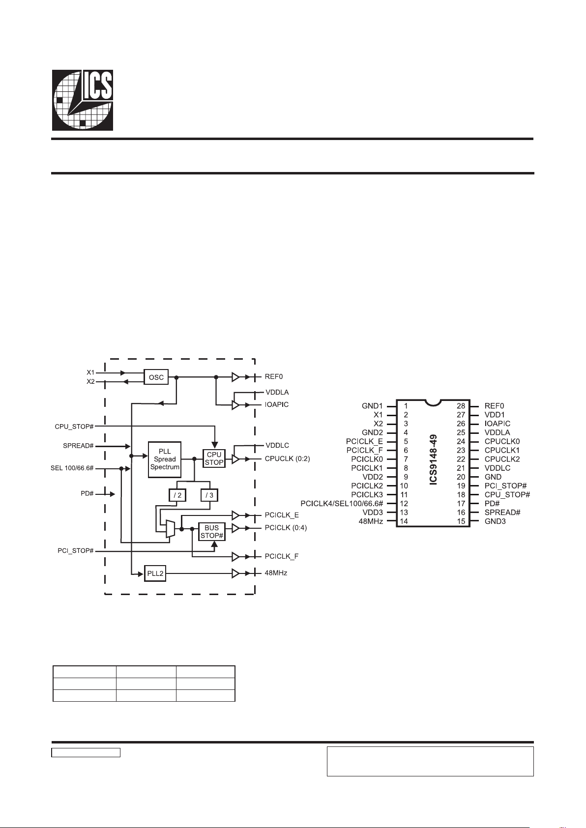
ICS9148-49
Block Diagram
Pentium/ProTM System Clock Chip
9148-49 Rev D 1/12/99
Pin Configuration
28-pin SSOP (209mil body)
Pentium is a trademark on Intel Corporation.
3CPUs @2.5V, up to 100MHz.
7PCIs @3.3V(including 1 free running, 1 Early).
1-48MHz(@3.3V) fixed.
1 REF(3.3V, 14.318MHz), 1 IOAPIC(2.5V, 14.318MHz)
Strong REF clock (1V/ns @ 50pf load)
Excellent power management features including Power
down, PCI and CPU stops
Spread Spectrum for EMI control(0.5% down spread)
Early PCI (3.0ns ±250ps)
The ICS9148-49 is part of a reduced pin count two-chip clock
solution for designs using an Intel BX style chipset.
Companion SDRAM buffers are ICS9179-03, -04 and -12.
There are two PLLs, with the first PLL capable of spread
spectrum operation. Spread spectrum typically reduces system
EMI by 8-10dB. The second PLL provides support for USB
48MHz requirements. CPU frequencies up to 100MHz are
supported.
Ground Groups
GND1=REF0, X1, PLL CORE, X2, IOAPIC
GND2=PCICLK_E, PCICLK_F, PCICLK(04)
GND=CPUCLK
GND3 = 48MHz
Power Groups
VDD1=REF0, X1, X2
VDD2=PCICLK_E , PCICLK_F , PCICLK(0:4)
VDD3=48MHz
VDDLC=CPUCLK(0:2)
VDDLA=IOAPIC
#6.66/001LES
zHMUPCzHMICP
10013.33
06.663.33
Frequency Table:
ICS reserves the right to make changes in the device data identified in
this publication without further notice. ICS advises its customers to
obtain the latest version of all device data to verify that any
information being relied upon by the customer is current and accurate.

2
ICS9148-49
Pin Descriptions
REBMUNNIPEMANNIPEPYTNOITPIRCSED
11DNGRWP.2X,1X,stuptuoFERrofdnuorG
21XNI
daolFp33lanretnisah,tupnilatsyrCzHM813.41NI_LATX
2Xmorfrotsiserkcabdeefdnapac
32XTUOFp33pacdaollanretnisah,tuptuolatsyrCTUO_LATX
42DNGRWPstuptuoICProfdnuorG
5E_KLCICPTUO
toN.sp052±sn2yb)F_,4:0(KLCICPsdaeL.KLCICPylraE
#POTS_ICPybdetceffa
6F_KLCICPTUO#POTS_ICPybdetceffatoNo.tuptuoICPgninnuReerF
11,01,8,7)3:0(KLCICPTUOV3.3elbitapmocLTT.stuptuokcolcICP
92DDVRWPV3.3yllanimon,stuptuoKLCICProfrewoP
21
4_KLCICPTUOV3.3elbitapmocLTT.tuptuokcolcICP
#6.66/001LESNI
zHM6.66rozHM001gnilbanerofniptceleS
)zHM3.33suonorhcnyssyawlaICP(zHM6.66=L,zHM001=H
313DDVRWPzHM84rofrewoP
41zHM84TUOzHM84@tuptuoKLCdexiF
513DNGRWPzHM84rofdnuorG
61#DAERPSNI1.daerpsnwod%5.0.evitcanehwmurtcpSdaerpSnosnruT
71#DPNI.ffodenruteratuptuolla,sLLPlanretnI.pihcnwodsrewoP
81#POTS_UPCNI.wolsitupninehwlevel"0"cigolta)0:2(KLCUPCtlaH
91#POTS_ICPNI
seoD.woltupninehwlevel"0"cigolta)4:0(KLCICPstlaH
F_KLCICP7E_KLCICPtceffaton
02DNGRWPerocLLProfdnuorG
12CLDDVRWPV5.2yllanimon,stuptuoUPCrofrewoP
42,32,22)0:2(KLCUPCTUOV5.2yllanimonstuptuokcolctsoHdnaUPC
62CIPAOITUO.zHM813.41tuptuokcolcCIPAOI
52ALDDVRWPCIPAOIrofrewoP
721DDVRWP.stuptuoFERrofrewoP
820FERTUO.purewoptatupnidehctaL/tuptuokcolczHM813.41

3
ICS9148-49
PCI_STOP# Timing Diagram
PCI_STOP# is an asynchronous input to the ICS9148-49. It is used to turn off the PCICLK (0:5) clocks for low power operation.
PCI_STOP# is synchronized by the ICS9148-49 internally. PCICLK (0:5) clocks are stopped in a low state and started with a full
high pulse width guaranteed. PCICLK (0:5) clock on latency cycles are only one rising PCICLK clock off latency is one PCICLK
clock.
CPU_STOP# Timing Diagram
CPUS_TOP# is an asychronous input to the clock synthesizer. It is used to turn off the CPUCLKs for low power operation.
CPU_STOP# is synchronized by the ICS9148-49. All other clocks will continue to run while the CPUCLKs clocks are disabled.
The CPUCLKs will always be stopped in a low state and start in such a manner that guarantees the high pulse width is a full
pulse. CPUCLK on latency is less than 4 CPUCLKs and CPUCLK off latency is less than 4 CPUCLKs.
Notes:
1. All timing is referenced to the internal CPUCLK.
2. CPU_STOP# is an asynchronous input and metastable conditions may exist.
This signal is synchronized to the CPUCLKs inside the ICS9148-49.
3. All other clocks continue to run undisturbed including SDRAMR.
4. PD# and PCI_STOP# are shown in a high (true) state.
Notes:
1. All timing is referenced to the Internal CPUCLK (defined as inside the ICS9148 device.)
2. PCI_STOP# is an asynchronous input, and metastable conditions may exist. This signal is required to be synchronized
inside the ICS9148.
3. All other clocks continue to run undisturbed.
4. PD# and CPU_STOP# are shown in a high (true) state.
 Loading...