Integrated
Circuit
Systems, Inc.
General Description Features
ICS9148-13
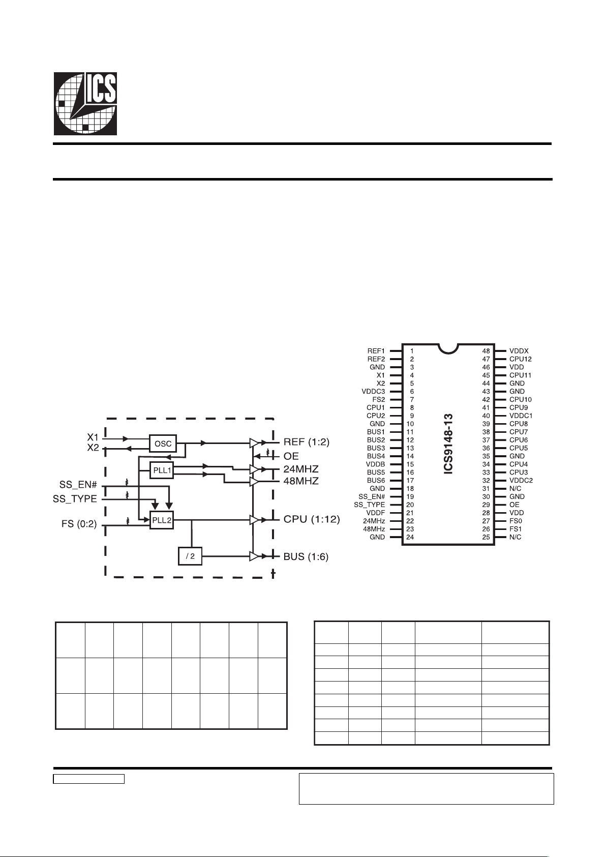
Block Diagram
Pentium is a trademark of Intel Corporation
Frequency Generator & Integrated Buffers for PENTIUM
TM
9148-13 Rev A 020398
Pin Configuration
The ICS9148-13 generates all clocks required for high speed
RISC or CISC microprocessor systems such as Intel Pentium
and PentiumPro. An output enable is provided for testability.
Spread Spectrum is available to modulate the CPU and BUS
PLL (leaving the REF, 24, 48 MHz operating normally). The
SS_EN# pin enables the spreading when low. The SS_TYPE
pin choses ±0.5% (nominally) center spread or +0, -2%
(nominally) downspread modulation.
High drive BUS outputs typically provide greater than 1 V/ns
slew rate into 30 pF loads. CPU outputs typically provide
better than 1V/ns slew rate into 20pF loads while maintaining
50 ±
5% duty cycle. The REF clock outputs typically provide
better than 0.8/ns slew rates.
Generates twelve processor, six bus, two
14.31818 MHz, 24MHz and one 48MHz clock for
USB support.
Synchronous clocks skew matched to 250ps window
on CPUs and 500ps window on BUSs
• CPU to BUS skew, 3.0 to 5.0ns (CPU Early)
3.0V - 3.7V supply range
48-pin SSOP package
48-Pin SSOP
Functionality
2SF1SF0SF
ni)21:1(UPC
zHM
ni)6:1(SUB
zHM
000 575.73
001 0013.33
010 570.03
011 3.3856.14
100 0552
101 0603
110 76.6633.33
111 555.72
EOFER
42
)zHM(
84
)zHM(
UPCSUBOCVCSO
1snuRsnuRsnuRsnuRsnuRsnuRsnuR
0
-irT
etats
-irT
etats
-irT
etats
-irT
etats
-irT
etats
snuRsnuR
Output Enable
30K pullup resistor to VDD on OE, FS(0:2), SS_EN#, SS_TYPE
ICS reserves the right to make changes in the device data identified in this
publication without further notice. ICS advises its customers to obtain the latest
version of all device data to verify that any information being relied upon by the
customer is current and accurate.

2
ICS9148-13
Pin Descriptions
Spread Spectrum Functionality
91niPtupnI
#NE_SS
02niPtupnI
EPYT_SS
MARDS,UPC
SKCOLCICPdna
CIPAOI,FERzHM42zHM84
0
0
nidetaludomycneuqerF
edommurtcepsdaerps
)yllanimon(%5.0-,%5.0+
zHM813.41zHM42zHM84
1
nidetaludomycneuqerF
edommurtcepsdaerps
)yllanimon(%0.2-,%0+
zHM813.41zHM42zHM84
1X
ycneuqerfydaetS,lamroN
edom
zHM813.41zHM42zHM84
REBMUNNIPEMANNIPEPYTNOITPIRCSED
2,12FER,1FERTUO.stuptuokcolcecnereferzHM813.41
,01,3,42,81
44,34,53,03
DNGRWPdnuorGeciveD
41XNI.tupnikcolclanretxerolatsyrC
52XTUO)detcennocnuevaelkcolcecnereferlanretxerof(.tuptuolatsyrC
6DDVRWPV3.3tlov.ylppusrewopO/I
72,62,7)2:0(SFNIsrotsiserpullupsaH.elbattsilnoitcnufeeS.stupnitcelesycneuqerF
71,61,41,31,21,11)6:1(SUBTUO.stuptuokcolcSUB
91#NE_SSNI.elbane=woL.elbanEmurtcepSdaerpS
02EPYT_SSNI
.daerpsnwodmurtcepSdaerpS=hgiH
.daerpsretnecmurtcepSdaerpS=woL
,23,13,82,12,51
84,64,04
DDVRWPV3.3.ylppusrewoperoC
22zHM42TUOtuptuokcolczHM42
32zHM84TUO.tuptuokcolczHM84
52C/NtcennocoN
92EONI
UPC,skcolCdexiF,skcolCsuBllawoLsilangissihtnehwelbanEtuptuO
)pudellupyllanretni(edometatsirtnidecalpstuptuoskcolC
,83,73,63,43,33
,8,74,54,24,14,93
9
)21:1(UPCTUO
ycneuqerfrofelbatytilanoitcnufeesstuptuoskcolcUPC
snoitacificeps
VDD Pins: 48, REFs, XT AL OSC
VDD Pins: 6, CPU 1- 2
VDD Pins: 15, BUS 1-6
VDD Pins: 24, 48, Fix PLL
VDD Pins: 28, CPU PLL CORE
VDD Pins: 32, CPU 3-6
VDD Pins: 40, CPU 7-10
VDD Pins: 46, CPU 11-12

3
ICS9148-13
Absolute Maximum Ratings
Supply Voltage. . . . . . . . . . . . . . . . . . . . . . . . . . . 7.0 V
Logic Inputs. . . . . . . . . . . . . . . . . . . . . . . . . . . . . GND –0.5 V to VDD +0.5 V
Ambient Operating Temperature . . . . . . . . . . . . 0°C to +70°C
Storage Temperature . . . . . . . . . . . . . . . . . . . . . . –65°C to +150°C
Stresses above those listed under Absolute Maximum Ratings may cause permanent damage to the device. These ratings are
stress specifications only and functional operation of the device at these or any other conditions above those listed in the
operational sections of the specifications is not implied. Exposure to absolute maximum rating conditions for extended periods
may affect product reliability.
Electrical Characteristics - Input/Supply/Common Output Parameters
TA = 0 - 70C; Supply V oltage VDD = 3.3 V +/-5% ( unless other wi se state d)
PARAMETER SYMBOL CONDITIONS MIN TYP MAX UNITS
Input High Vol ta ge V
IH
2V
DD
+0.3 V
In put Low Vol ta ge V
IL
VSS-0.3 0.8 V
Input High Curr en t I
IH1
VIN = V
DD;
SS_Type o nly 6 8.0 200
µ
A
I
IH2
VIN = V
DD;
Al l outputs Except SS_Type -5 0.2 5
µ
A
Input Low Current I
IL1
VIN = 0 V;with pull-down resistors SS_Type only
-5 0.2 5
µ
A
I
IL2
VIN = 0 V;with pull-up resistors except SS_Type
-200 -100
µ
A
Supply Current I
DD
CL = 0 pF; Select @ 66M 67 180 mA
Input freque nc y F
i
VDD = 3.3 V; 14.318 MHz
Input Capac itance
1
C
IN
Logi c Inputs 5 pF
C
INX
X1 & X2 pins 27 36 45 pF
Transition Time
1
T
trans
To 1st crossi ng of target Freq. 1 .5 3 ms
Clk Stabilization
1
T
STAB
From VDD = 3.3 V to 1% target Freq. 3 ms
Skew
1
T
CPU-BUSVT
= 1.5 V;
3.0 4.0 5.0 ns
1
Guarente ed by design, not 1 00 % tested i n production.
 Loading...