

Integrated
Circuit
Systems, Inc.
General Description Features
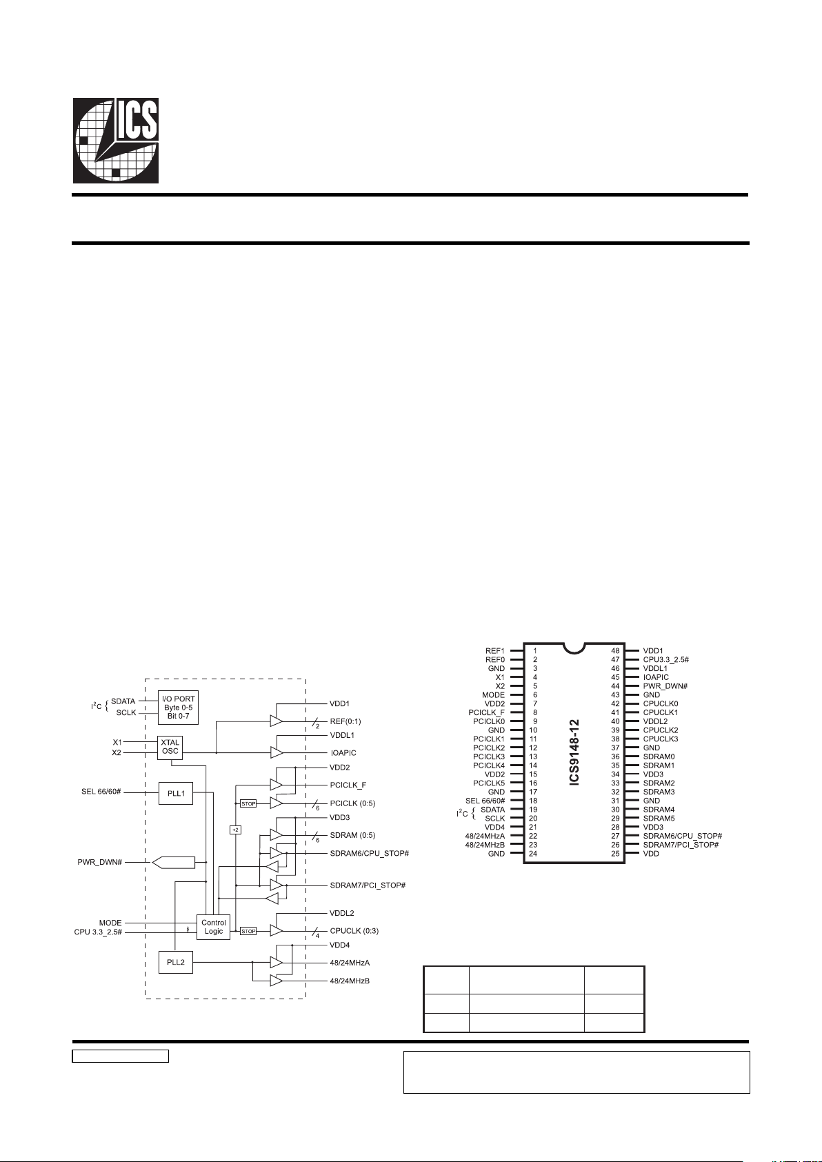
ICS9148-12
Block Diagram
Pentium/ProTM System Clock Chip
9148-12 Rev F 4/1/99
Pentium is a trademark on Intel Corporation.
CPU outputs are stronger drive for multiple loads per pin
(ie CPU and NB on one pin)
Generates system clocks for CPU, IOAPIC, SDRAM,
PCI, plus 14.314 MHz REF(0:1), USB, Plus Super I/O
Supports single or dual processor systems
I2C serial configuration interface provides output clock
disabling and other functions
MODE input pin selects optional power management
input control pins
Two fixed outputs separately selectable as 24 or 48MHz
Separate 2.5V and 3.3V supply pins
2.5V or 3.3V outputs: CPU, IOAPIC
3.3V outputs: SDRAM, PCI, REF, 48/24 MHz
CPU 3.3_2.5# logic pin to adjust output strength
No power supply sequence requirements
Uses external 14.318MHz crystal
48 pin 300 mil SSOP and 240 mil TSSOP
Output enable register
for serial port control: 1 = enable
0 = disable
The ICS9148-12 is a Clock Synthesizer chip for Pentium and
PentiumPro CPU based Desktop/Notebook systems that will
provide all necessary clock timing.
Features include four strong CPU, seven PCI and eight
SDRAM clocks. Two reference outputs are available equal to
the crystal frequency. Stronger drive CPUCLK outputs
typically provide greater than 1 V/ns slew rate into 20pF
loads. This device meets rise and fall requirements with 2
loads per CPU output (ie, one clock to CPU and NB chipset,
one clock to two L2 cache inputs).
PWR_DWN# pin allows low power mode by stopping crystal
OSC and PLL stages. For optional power management,
CPU_STOP# can stop CPU (0:3) clocks and PCI_STOP#
will stop PCICLK (0:5) clocks. CPU and IOAPIC output
buffer strength controlled by CPU 3.3_2.5# pin to match
VDDL voltage.
PCICLK outputs typically provide better than 1V/ns slew rate
into 30pF loads while maintaining 50±5% duty cycle. The REF
clock outputs typically provide better than 0.5V/ns slew rates.
The ICS9148-12 accepts a 14.318MHz reference crystal or
clock as its input and runs on a 3.3V core supply.
Functionality
VDD (1:4) 3.3V±10%, VDDL1, 2 2.5±5% or 3.3±10% 0-70°C
Crystal (X1, X2) = 14.31818 MHz
LES
MARDS,KLCUPC
)zHM(
KLCICP
)zHM(
00603
16.663.33
Pin Configuration
48-Pin SSOP & TSSOP
ICS reserves the right to make changes in the device data identified in this
publication without further notice. ICS advises its customers to obtain the latest
version of all device data to verify that any information being relied upon by the
customer is current and accurate.
2
ICS9148-12
Pin Descriptions
Power Groups
VDD = Supply for PLL core
VDD1 = REF (0:1), X1, X2
VDD2 = PCICLK_F, PCICLK (0:5)
VDD3 = SDRAM (0:5), SDRAM6/CPU_STOP#, SDRAM7/PCI_STOP#
VDD4 = 48/24MHzA, 48/24MHzB
VDDL1 = IOAPIC
VDDL2 = CPUCLK (0:3)
REBMUNNIPEMANNIPEPYTNOITPIRCSED
1,2)1:0(FERTUOtuptuOkcolcecnerefeR
,42,71,01,3
34,73,13
DNGRWP)nommoc(dnuorG
41XNIpacdaollatsyrclanretnisah,tupniecnereferrolatsyrC
52XTUO
kcabdeefdnapacdaollanretnisah,tuptuolatsyrC
1Xotrotsiser
6EDOMNInoitcelesnoitcnuftupnI
51,72DDVRWPV3.3lanimon,)5:0(KLCICP,F_KLCICProfylppuS
8F_KLCICPTUO#POTS_ICPybdetceffaton,kcolcICPgninnureerF
61,41,31,21,11,9)5:0(KLCICPTUOskcolcICP
81#06/66LESNIUPCdnaMARDSrofzHM6.66rozHM06stceleS
91ATADSNII
2
tupniatadC
02KLCSNII
2
tupnikcolcC
124DDVRWPV3.3lanimon,BzHM42/84,AzHM42/84rofylppuS
22AzHM42/84TUOO/IrepuSroBSUroftuptuorevirdzHM42/84
32BzHM42/84TUOO/IrepuSroBSUroftuptuorevirdzHM42/84
52DDVRWPV3.3lanimon,erocLLProfylppuS
62
7MARDSTUO)detceles(zHM6.66/06kcolcMARDS
#POTS_ICPNIwolnehwlevel"0"cigolta)5:0(suBICPstlaH
72
6MARDSTUO)detceles(zHM6.66/06kcolcMARDS
#POTS_UPCNIwolnehwlevel"0"cigoltaskcolcUPCstlaH
43,823DDVRWP
,#POTS_UPC/6MARDS,)5:0(MARDSrofylppuS
V3.3lanimon,#POTS_ICP/7MARDS
042LDDVRWPlanimonV3.3ro5.2rehtie,)3:0(KLCUPCrofylppuS
83,93,14,24)3:0(KLCUPCTUO2LDDVybderewop,tuptuokcolcKLCUPC
92,03,23,33,53,63)5:0(MARDSTUO)detceles(zHM6.66ro06takcolcsMARDS
44#NWD_RWPNIwolevitca,pihcnwodsrewoP
54CIPAOITUO1LDDVybderewop)zHM813.41(,tuptuokcolcCIPAOI
641LDDVRWPlanimonV3.3ro5.2rehtie,CIPAOIrofylppuS
74#5.2-3.3UPCNI
,DDVotpullupsah,noitceleshtgnertsreffubDDV5.2ro3.3
.rotsiserK03lanimon
841DDVRWPV3.3lanimon,2X,1X,)1:0(FERrofylppuS
3
ICS9148-12
Power-On Conditions
Example:
a) if MODE = 1, pins 26 and 27 are configured as SDRAM7 and SDRAM6 respectively.
b) if MODE = 0, pins 26 and 27 are configured as PCI_STOP# and CPU_STOP# respectively.
Power-On Default Conditions
At power-up and before device programming, all clocks will default to an enabled and on condition. The frequencies that are then produced
are on the MODE pin as shown in the table below.
KCOLC PU-REWOPTANOITIDNOCTLUAFED
)1:0(FER zHM81813.41
0CIPAOI zHM81813.41
zHM42/84zHM84
#06/66LESEDOM#NIPNOITPIRCSEDNOITCNUF
11
24,14,93,83sKLCUPCelbasid/elbanegifnoclaires/w-zHM6.66
,23,33,53,63
62,72,92,03
MARDSstuptuoMARDSllA-zHM6.66
,21,31,41,61
8,9,11
sKLCICPelbasid/elbanegifnoclaires/w-zHM3.33
01
24,14,93,83sKLCUPCelbasid/elbanegifnoclaires/w-zHM06
,23,33,53,63
62,72,92,03
MARDSelbasid/elbanegifnoclaires/w-zHM06
,21,31,41,61
8,9,11
sKLCICPelbasid/elbanegifnoclaires/w-zHM03
10
62#POTS_ICP
skcolC)5:0(ICP,tnemeganaMrewoP
wolnehwdeppotS
72#POTS_UPC
skcolC)5:0(UPC,tnemeganaMrewoP
wolnehwdeppotS
8F_KLCICP
rofgninnureerFkcolCICP-zHM3.33-zHM3.33
tnemeganaMrewoP
24,14,93,83sKLCUPC
dnalortnoCpotSlanretxe/wskcolCUPC-zHM6.66
.elbasid/elbanelaudividnigifnoclaires
,23,33,53,63
92,03
MARDS
laudividnigifnoclaires/wskcolCMARDS-zHM6.66
.elbasid/elbane
,21,31,41,61
9,11
sKLCICP
dnalortnocpotSlanretxe/wskcolCICP-zHM3.33
.elbasid/elbanelaudividnigifnoclaires
00
62#POTS_ICP
skcolC)5:0(ICP,tnemeganaMrewoP
wolnehwdeppotS
72#POTS_UPC
skcolC)5:0(UPC,tnemeganaMrewoP
wolnehwdeppotS
8F_KLCICP
rewoProfgninnureerFkcolCICP-zHM03
tnemeganaM
24,14,93,83sKLCUPC
dnalortnocpotSlanretxe/wskcolCUPC-zHM06
.elbasid/elbanelaudividnigifnoclaires
,23,33,53,63
92,03
MARDS
laudividnigifnoclaires/wskcolCMARDS-zHM06
.elbasid/elbane
,21,31,41,61
9,11
sKLCICP
dnalortnocpotSlanretxe/wskcolCICP-zHM03
.elbasid/elbanelaudividnigifnoclaires

4
ICS9148-12
T echnical Pin Function Descriptions
VDD(1,2,3,4)
This is the power supply to the internal core logic of the
device as well as the clock output buffers for REF(0:1),
PCICLK, 48/24MHzA/B and SDRAM(0:7).
This pin operates at 3.3V volts. Clocks from the listed
buffers that it supplies will have a voltage swing from Ground
to this level. For the actual guaranteed high and low voltage
levels for the Clocks, please consult the DC parameter table
in this data sheet.
VDDL1,2
This is the power supplies for the CPUCLK and IOAPCI
output buffers. The voltage level for these outputs may be
2.5 or 3.3volts. Clocks from the buffers that each supplies
will have a voltage swing from Ground to this level. For the
actual Guaranteed high and low voltage levels of these
Clocks, please consult the DC parameter table in this Data
Sheet.
GND
This is the power supply ground (common or negative) return
pin for the internal core logic and all the output buffers.
X1
This input pin serves one of two functions. When the device
is used with a Crystal, X1 acts as the input pin for the
reference signal that comes from the discrete crystal. When
the device is driven by an external clock signal, X1 is the
device input pin for that reference clock. This pin also
implements an internal Crystal loading capacitor that is
connected to ground. See the data tables for the value of this
capacitor.
X2
This Output pin is used only when the device uses a Crystal
as the reference frequency source. In this mode of operation,
X2 is an output signal that drives (or excites) the discrete
Crystal. The X2 pin will also implement an internal Crystal
loading capacitor that is connected to ground. See the Data
Sheet for the value of this capacitor.
CPUCLK (0:3)
These Output pins are the Clock Outputs that drive processor
and other CPU related circuitry that requires clocks which
are in tight skew tolerance with the CPU clock. The voltage
swing of these Clocks are controlled by the Voltage level
applied to the VDDL2 pin of the device. See the Functionality
Table for a list of the specific frequencies that are available
for these Clocks and the selection codes to produce them.
SDRAM(0:7)
These Output Clocks are use to drive Dynamic RAMs and
are low skew copies of the CPU Clocks. The voltage swing
of the SDRAMs output is controlled by the supply voltage
that is applied to VDD3 of the device, operates at 3.3 volts.
48/24MHzA, B
This is a fixed frequency Clock output that is typically used
to drive Super I/O devices. Outputs A and B are defined as
24 or 48MHz by I2C register (see table).
IOAPIC
This Output is a fixed frequency Output Clock that runs at the
Reference Input (typically 14.31818MHz) . Its voltage level
swing is controlled by VDDL1 and may operate at 2.5 or
3.3volts.
REF(0:1)
The REF Outputs are fixed frequency Clocks that run at the
same frequency as the Input Reference Clock X1 or the
Crystal (typically 14.31818MHz) attached across X1 and
X2.
PCICLK_F
This Output is equal to PCICLK(0:5) and is FREE RUNNING,
and will not be stopped by PCI_STP#.
PCICLK (0:5)
These Output Clocks generate all the PCI timing requirements
for a Pentium/Pro based system. They conform to the
current PCI specification. They run at 1/2 CPU frequency.
SELECT 66.6/60MHz#
This Input pin controls the frequency of the Clocks at the
CPU, PCICLK and SDRAM output pins. If a logic 1 value
is present on this pin, the 66.6 MHz Clock will be selected.
If a logic 0 is used, the 60MHz frequency will be selected.
MODE
This Input pin is used to select the Input function of the I/
O pins. An active Low will place the I/O pins in the Input
mode and enable those stop clock functions.

5
ICS9148-12
CPU3.3_2.5#
This Input pin controls the CPU and IOAPIC output buffer
strength for skew matching CPU and SDRAM outputs to
compensate for the external VDDL supply condition. It is
important to use this function when selecting power supply
requirements for VDDL1,2. A logic 0 (ground) will indicate
2.5V operation and a logic 1 will indicate 3.3V operation.
This pin has an internal pullup resistor to VDD.
PWR_DWN#
This is an asynchronous active Low Input pin used to Power
Down the device into a Low Power state by not removing the
power supply. The internal Clocks are disabled and the VCO
and Crystal are stopped. Powered Down will also place all
the Outputs in a low state at the end of their current cycle.
The latency of Power Down will not be greater than 3ms. The
I2C inputs will be Tri-Stated and the device will retain all
programming information. This input pin only valid when
MODE=0 (Power Management Mode)
CPU_STOP#
This is a synchronous active Low Input pin used to stop the
CPUCLK clocks in an active low state. All other Clocks
including SDRAM clocks will continue to run while this
function is enabled. The CPUCLKs will have a turn ON
latency of at least 3 CPU clocks. This input pin only valid
when MODE=0 (Power Management Mode)
PCI_STOP#
This is a synchronous active Low Input pin used to stop the
PCICLK clocks in an active low state. It will not effect
PCICLK_F nor any other outputs. This input pin only valid
when MODE=0 (Power Management Mode)
I2C
The SDATA and SCLOCK Inputs are use to program the
device. The clock generator is a slave-receiver device in the
I2C protocol. It will allow read-back of the registers. See
configuration map for register functions. The I2C
specification in Philips I2C Peripherals Data Handbook
(1996) should be followed.
T echnical Pin Function Descriptions
6
ICS9148-12
1. The ICS clock generator is a slave/receiver, I2C component. It can read back the data stored in the latches for verification.
Read-Back will support Intel PIIX4 "Block-Read" protocol.
2. The data transfer rate supported by this clock generator is 100K bits/sec or less (standard mode)
3. The input is operating at 3.3V logic levels.
4. The data byte format is 8 bit bytes.
5. To simplify the clock generator I2C interface, the protocol is set to use only "Block-Writes" from the controller. The
bytes must be accessed in sequential order from lowest to highest byte with the ability to stop after any complete byte
has been transferred. The Command code and Byte count shown above must be sent, but the data is ignored for those
two bytes. The data is loaded until a Stop sequence is issued.
6. At power-on, all registers are set to a default condition, as shown.
General I2C serial interface information
The information in this section assumes familiarity with I2C programming.
For more information, contact ICS for an I2C programming application note.
How to Write:
Controller (host) sends a start bit.
Controller (host) sends the write address D2
(H)
ICS clock will acknowledge
Controller (host) sends a dummy command code
ICS clock will acknowledge
Controller (host) sends a dummy byte count
ICS clock will acknowledge
Controller (host) starts sending first byte (Byte 0)
through byte 5
ICS clock will acknowledge each byte one at a time.
Controller (host) sends a Stop bit
How to Read:
Controller (host) will send start bit.
Controler (host) sends the read address D3
(H)
ICS clock will acknowledge
ICS clock will send the byte count
Controller (host) acknowledges
ICS clock sends first byte (Byte 0) through byte 5
Controller (host) will need to acknowledge each byte
Controller (host) will send a stop bit
Notes:
Controller (Host) ICS (Slave/Receiver)
Start Bit
Address
D3
(H)
AC
K
Byte Count
ACK
Byte
0
ACK
Byte 1
ACK
Byte
2
ACK
Byte
3
ACK
Byte 4
ACK
Byte
5
ACK
Stop Bit
How to Read:
Controller (Host) ICS (Slave/Receiver)
Start Bit
Address
D2
(H)
AC
K
Dummy Command Code
AC
K
Dummy Byte Count
AC
K
Byte 0
AC
K
Byte 1
ACK
Byte 2
AC
K
Byte 3
AC
K
Byte 4
AC
K
Byte 5
AC
K
Stop Bit
How to Write:

7
ICS9148-12
Notes:
1. TCLK is a test clock driven on the X1 (crystal in pin) input during test mode.
ytilanoitcnuFUPC
,ICP
F_ICP
MARDSFERCIPAOI
zHM42
noitceleS
zHM84
noitceleS
etatsirTZ-IHZ-IHZ-IHZ-IHZ-IHZ-IHZ-IH
edomtseT2/KLCT
1
4/KLCT
1
2/KLCT
1
KLCT
1
KLCT
1
4/KLCT
1
2/KLCT
1
Select Functions
Serial Configuration Command Bitmaps
Byte 0: Functional and Frequency Select Clock Register (default on Bits 7, 6, 5, 4, 1, 0 = 0)
(default on Bits 3, 2 = 1)
Note: PWD = Power-Up Default
TIB#NIPNOITPIRCSEDDWP
7tiB- devreseR0
6tiB- noitarepolamronrof0ebtsuM0
5tiB-
epytslortnoC,murtcepSdaerpSnI
)daerpsnwod=1,deretnec=0(
0
4tiB
gnidaerpSslortnoC,murtcepSdaerpSnI
)%6.0=1%8.1=0(
0
3tiB32zHM42=0,zHM84=1)tceleSycneuqerF(zHM42/841
2tiB22zHM42=0,zHM84=1)tceleSycneuqerF(zHM42/841
1tiB
0tiB
-
1tiB
1
1
0
0
0tiB
etatS-irT-1
elbanEmurtcepSdaerpS-0
edomtseT-1
noitarepolamroN-0
0
0

8
ICS9148-12
Byte 1: CPU, 24/48 MHz Clock Register
Notes: 1 = Enabled; 0 = Disabled, outputs held low
Byte 2: PCICLK Clock Register
Byte 4: SDRAM Clock Register
Notes: 1 = Enabled; 0 = Disabled, outputs held low
Notes: 1 = Enabled; 0 = Disabled, outputs held low
TIB#NIPDWPNOITPIRCSED
7tiB-1 devreseR
6tiB81 )tcanI/tcA(F_KLCICP
5tiB611 )tcanI/tcA(5KLCICP
4tiB411 )tcanI/tcA(4KLCICP
3tiB311 )tcanI/tcA(3KLCICP
2tiB211 )tcanI/tcA(2KLCICP
1tiB111 )tcanI/tcA(1KLCICP
0tiB91 )tcanI/tcA(0KLCICP
TIB#NIPDWPNOITPIRCSED
7tiB-1 devreseR
6tiB-1 devreseR
5tiB-1 devreseR
4tiB-1 devreseR
3tiB-1 devreseR
2tiB-1 devreseR
1tiB-1 devreseR
0tiB-1 devreseR
TIB#NIPDWPNOITPIRCSED
7tiB321 )tcanI/tcA(zHM42/84
6tiB221 )tcanI/tcA(zHM42/84
5tiB-1 devreseR
4tiB-1 devreseR
3tiB831 )tcanI/tcA(3KLCUPC
2tiB931 )tcanI/tcA(2KLCUPC
1tiB141 )tcanI/tcA(1KLCUPC
0tiB241 )tcanI/tcA(0KLCUPC
Byte 3: SDRAM Clock Register
Notes: 1 = Enabled; 0 = Disabled, outputs held low
TIB#NIPDWPNOITPIRCSED
7tiB621 )tcanI/tcA(7MARDS
6tiB721 )tcanI/tcA(6MARDS
5tiB921 )tcanI/tcA(5MARDS
4tiB031 )tcanI/tcA(4MARDS
3tiB231 )tcanI/tcA(3MARDS
2tiB331 )tcanI/tcA(2MARDS
1tiB531 )tcanI/tcA(1MARDS
0tiB631 )tcanI/tcA(0MARDS
Note: PWD = Power-Up Default
Byte 5: Peripheral Clock Register
Notes: 1 = Enabled; 0 = Disabled, outputs held low
TIB#NIPDWPNOITPIRCSED
7tiB-1 devreseR
6tiB-1 devreseR
5tiB-1 devreseR
4tiB541 )tcanI/tcA(0CIPAOI
3tiB-1 devreseR
2tiB-1 devreseR
1tiB11 )tcanI/tcA(1FER
0tiB21 )tcanI/tcA(0FER
Note: PWD = Power-Up Default
Byte 6: Optional Register for Future
Notes:
1. Byte 6 is reserved by Integrated Circuit Systems for
future applications.
TIB#NIPDWPNOITPIRCSED
7tiB-1 devreseR
6tiB-1 devreseR
5tiB-1 devreseR
4tiB-1 devreseR
3tiB-1 devreseR
2tiB-1 devreseR
1tiB-1 devreseR
0tiB-1 devreseR

9
ICS9148-12
Power Management
ICS9148-12 Power Management Requirements
Clock Enable Configuration
Full clock cycle timing is guaranteed at all times after the system has initially powered up except where noted. During power
up and power down operations using the PWR PD# select pin will not cause clocks of a short or longer pulse than that of the
running clock. The first clock pulse coming out of a stopped clock condition may be slightly distorted due to clock network
charging circuitry. Board routing and signal loading may have a large impact on the initial clock distortion also.
Notes.
1. Clock on latency is defined from when the clock enable goes active to when the first valid clock comes out of the device.
2. Clock off latency is defined from when the clock enable goes inactive to when the last clock is driven low out of the device.
3. Power up latency is when PD# goes inactive (high) to when the first valid clocks are output by the device.
4. Power down has controlled clock counts applicable to CPUCLK, SDRAM, PCICLK only.
The REF and IOAPIC will be stopped independant of these.
LANGISETATSLANGIS
ycnetaL
gninnureerffosegdegnisirfo.oN
KLCICP
#POTS_UPC)delbasiD(0
2
1
)delbanE(1
1
1
#POTS_ICP)delbasiD(0
2
1
)delbanE(1
1
1
#NWD_RWP)noitarepOlamroN(1
3
Sm3
)nwoDrewoP(0
4
xam2
#POTS_UPC#POTS_ICP#NWD_RWPKLCUPCKLCICP
,skcolCrehtO
,MARDS
,FER
,sCIPAOI
AzHM42/84
BzHM42/84
latsyrCsOCV
XX 0 woLwoLdeppotSffOffO
00 1 woLwoLgninnuRgninnuRgninnuR
011 woLzHM03/3.33gninnuRgninnuRgninnuR
10 1 zHM06/6.66woLgninnuRgninnuRgninnuR
111 zHM06/6.66zHM03/3.33gninnuRgninnuRgninnuR
10
ICS9148-12
PCI_STOP# Timing Diagram
PCI_STOP# is an asynchronous input to the ICS9148-12. It is used to turn off the PCICLK (0:5) clocks for low power operation.
PCI_STOP# is synchronized by the ICS9148-12 internally. The minimum that the PCICLK (0:5) clocks are enabled (PCI_STOP#
high pulse) is at least 10 PCICLK (0:5) clocks. PCICLK (0:5) clocks are stopped in a low state and started with a full high pulse
width guaranteed. PCICLK (0:5) clock on latency cycles are only one rising PCICLK clock off latency is one PCICLK clock.
CPU_STOP# Timing Diagram
CPUSTOP# is an asychronous input to the clock synthesizer. It is used to turn off the CPUCLKs for low power operation.
CPU_STOP# is synchronized by the ICS9148-12. The minimum that the CPUCLK is enabled (CPU_STOP# high pulse) is 100
CPUCLKs. All other clocks will continue to run while the CPUCLKs are disabled. The CPUCLKs will always be stopped in a low
state and start in such a manner that guarantees the high pulse width is a full pulse. CPUCLK on latency is less than 4 CPUCLKs
and CPUCLK off latency is less than 4 CPUCLKs.
(Drawing shown on next page.)
Notes:
1. All timing is referenced to the internal CPUCLK.
2. CPU_STOP# is an asynchronous input and metastable conditions may exist.
This signal is synchronized to the CPUCLKs inside the ICS9148-12.
3. All other clocks continue to run undisturbed.
4. PD# and PCI_STOP# are shown in a high (true) state.

11
ICS9148-12
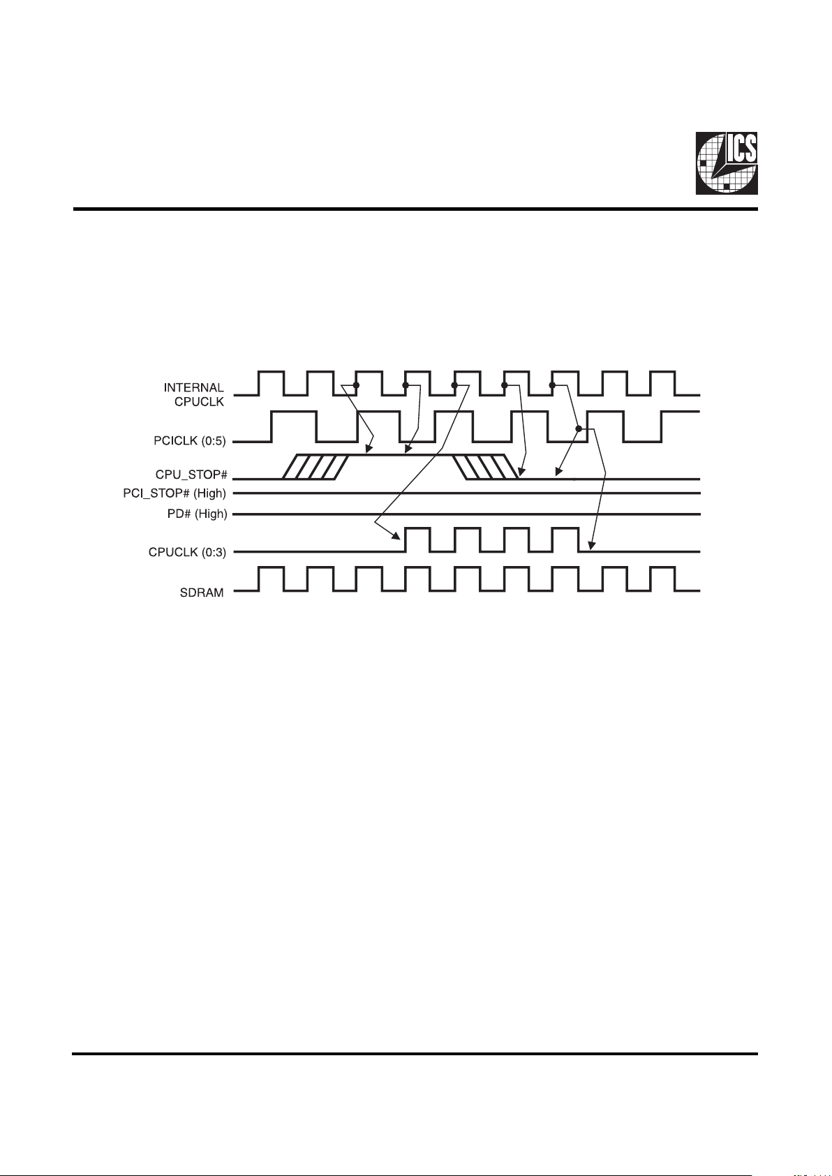
PD# Timing Diagram
The power down selection is used to put the part into a very low power state without turning off the power to the part. PD# is
an asynchronous active low input. This signal is synchronized internal by the ICS9148-12 prior to its control action of
powering down the clock synthesizer. Internal clocks will not be running after the device is put in power down state. When PD#
is active (low) all clocks are driven to a low state and held prior to turning off the VCOs and the Crystal oscillator. The power
on latency is guaranteed to be less than 3mS. The power down latency is less than three CPUCLK cycles. PCI_STOP# and
CPU_STOP# are dont care signals during the power down operations.
Notes:
1. All timing is referenced to the Internal CPUCLK (defined as inside the ICS9148 device).
2. PD# is an asynchronous input and metastable conditions may exist. This signal is synchronized inside the ICS9148.
3. The shaded sections on the VCO and the Crystal signals indicate an active clock is being generated.
Notes:
1. All timing is referenced to the Internal CPUCLK (defined as inside the ICS9148 device.)
2. PCI_STOP# is an asynchronous input, and metastable conditions may exist. This signal is required to be synchronized
inside the ICS9148.
3. All other clocks continue to run undisturbed.
4. PD# and CPU_STOP# are shown in a high (true) state.
12
ICS9148-12
Electrical Characteristics - Input/Supply/Common Output Parameters
TA = 0 - 70C; Supply Volta ge VDD = V
DDL
= 3. 3 V +/- 5% (unles s othe rw ise s tat ed)
PARAMETER SYMBOL CONDITIONS MIN TYP MAX UNITS
Input High Voltage V
IH
2V
DD
+0.3 V
Input Low Volta ge V
IL
VSS-0.3 0.8 V
Inpu t High C urrent I
IH
VIN = V
DD
0.1 5
µ
A
Input Low Current I
IL1
VIN = 0 V; Inputs with no pul l-up resi stor s -5 2. 0
µ
A
Input Low Current I
IL2
VIN = 0 V; Inputs with pul l-up r e sisto rs -200 -100
µ
A
Operating I
DD3.3OP
CL = 0 pF; S e lect @ 66M 60 100 mA
Suppl y C urrent
Power Down I
DD3.3PD
CL = 0 pF; With input a ddress to Vdd or GND 400 600
µ
A
Suppl y C urrent
Input fr e que ncy F
i
VDD = 3.3 V ; 14.318 MHz
Input Ca pa c itanc e
1
C
IN
Logic Inputs 5 pF
C
INX
X 1 & X2 pins 27 36 45 pF
Tr a nsition Tim e
1
T
trans
To 1st cr o s sing of target Freq. 3 ms
Se ttling Time
1
T
s
From 1 s t c rossing to 1% t a rget Fr e q. ms
Clk S tabiliz a tion
1
T
STA B
From VDD = 3. 3 V to 1% target Fr e q. 3 mS
Skew
1
T
CPU-SDRAM1VT
= 1 .5 V 200 500 ps
T
CPU-PCI1VT
= 1.5 V;
1.5 3.2 4.5 ns
1
G ua rente e d by design, no t 100 % teste d in producti on.
Electrical Characteristics - Input/Supply/Common Output Parameters
TA = 0 - 70C; Supply Voltage VDD = 3.3 V +/-5%, V
DDL
= 2.5 V +/-5% (unless otherwi se stated)
PARAMETER SYMBOL CONDITIONS MIN TYP MAX UNITS
Operating I
DD2.5OPCL
= 0 pF; Select @ 66M 5 20 mA
Supply Current
Power Down I
DD2.5PDCL
= 0 pF; 0.21 1.0
µ
A
Supply Current
Skew
1
T
CPU-SDRAM2VT
= 1.5 V; VTL = 1.25 V; SDRAM Leads 150 500 ps
T
CPU-P CI2VT
= 1.5 V; VTL = 1.25 V; CPU Leads
12.84ns
1
Guar e nt e ed by design, n ot 100% tested in production.
Absolute Maximum Ratings
Supply Voltage . . . . . . . . . . . . . . . . . . . . . . . . . . . 7.0 V
Logic Inputs . . . . . . . . . . . . . . . . . . . . . . . . . . . . GND 0.5 V to VDD +0.5 V
Ambient Operating Temperature . . . . . . . . . . . . 0°C to +70°C
Case Temperature . . . . . . . . . . . . . . . . . . . . . . . . 115°C
Storage Temperature . . . . . . . . . . . . . . . . . . . . . . 65°C to +150°C
Stresses above those listed under Absolute Maximum Ratings may cause permanent damage to the device. These ratings are
stress specifications only and functional operation of the device at these or any other conditions above those listed in the
operational sections of the specifications is not implied. Exposure to absolute maximum rating conditions for extended periods
may affect product reliability.

13
ICS9148-12
Electrical Characteristics - CPU
TA = 0 - 70C; VDD = V
DDL
= 3.3 V +/-5%; CL = 10 - 20 pF (unless otherwise stated)
PARAMETER SYMBOL CONDITIONS MIN TYP MAX UNITS
O ut put Freque nc y F
O2
60 66 MHz
O ut put Impedanc e R
DSP2A
1
VO = VDD*(0.5) 10 20
Ω
O ut put Impedanc e R
DSN2A
1
VO = VDD*(0.5) 10 20
Ω
O utput High Vol t ag e V
OH2A
IOH = -28 mA 2.4 2.5 V
Output Low Voltage V
OL2AIOL
= 27 mA 0.35 0.4 V
Ou t put High Current I
OH2A
VOH = 2.0 V -52 -48 mA
Output Low Current I
OL2A
VOL = 0.8 V 49.3 59 mA
Rise Time t
r2A
1
VOL = 0.4 V, VOH = 2.4 V 1.1 2.85 ns
Fall Time t
f2A
1
VOH = 2.4 V, VOL = 0.4 V 0.95 2.85 ns
Duty Cycle d
t2A
1
VT = 1.5 V 45 51 55 %
Skew t
sk2A
1
VT = 1.5 V 80 250 ps
t
jcyc-cyc2A
1
VT = 1.5 V 170 250 ps
Jitter t
j1s2A
1
VT = 1.5 V 60 150 ps
t
jabs2A
1
VT = 1.5 V
-250 100 +250 ps
1
Guar e nt eed by design, not 100% tested in production.
Electrical Characteristics - CPU
TA = 0 - 70C; VDD = 3.3 V +/-5%, V
DDL
= 2.5 V +/-5%; CL = 10 - 20 pF ( unless otherwise stated)
PARAMETER SYMBOL CONDITIONS MIN TYP MAX UNITS
O ut put Freque nc y F
O2
60 66 MHz
O ut put Impedanc e R
DSP2B
1
VO = VDD*(0.5) 10 20
Ω
O ut put Impedanc e R
DSN2B
1
VO = VDD*(0.5) 10 20
Ω
O utput High Vol t ag e V
OH2BIOH
= -8.0 mA 2.1 2.15 V
Output Low Voltage V
OL2B
IOL = 21 mA 0.3 0.4 V
Ou t put High Current I
OH2B
VOH = 1.8 V -22 -18 mA
Output Low Current I
OL2B
VOL = 0.5 V 33 36 mA
Rise Time t
r2B
1
VOL = 0.4 V, VOH = 2.0 V 1 .2 1.5 ns
Fall Time t
f2B
1
VOH = 2.0 V, VOL = 0.4 V 0.95 1.3 ns
Duty Cycle d
t2B
1
VT = 1.25 V 45 50 55 ns
Skew t
sk2B
1
VT = 1.25 V 60 250 ps
t
jcyc-cyc2B
1
VT = 1.25 V 150 250 ps
Jitter t
j1s2B
1
VT = 1.25 V 50 150 ps
t
jabs2B
1
VT = 1.25 V
-250 80 +250 ps
1
Guar e nt eed by design, not 100% tested in production.

14
ICS9148-12
Electrical Characterist ics - PCI
TA = 0 - 70C; VDD = V
DDL
= 3.3 V +/-5%; CL = 30 pF (unless other wise stat e d)
PARAMETER SYMBOL C ONDITIONS MIN TYP MAX UNITS
O ut put Freque nc y F
O1
30 - 33 MHz
O ut put Impedanc e R
DSP1
1
VO = VDD*(0.5) 12 55
Ω
O ut put Impedanc e R
DSN1
1
VO = VDD*(0.5) 12 55
Ω
O utput High Vol t a ge V
OH1
IOH = -14.5 mA 2.4 2.7 V
Output Low Voltage V
OL1
IOL = 9.4 mA 0.2 0.4 V
Ou t put High Current I
OH1
VOH = 2.0 V -47 -22 mA
Output Low Current I
OL1
VOL = 0.8 V 17.1 47.5 mA
Rise Time t
r1
1
VOL = 0.4 V, VOH = 2.4 V 1.5 2 ns
Fall Time t
f1
1
VOH = 2.4 V, VOL = 0.4 V 1.1 2 ns
Duty Cycle d
t1
1
VT = 1.5 V 45 51 55 %
Skew t
sk1
1
VT = 1.5 V 100 250 ps
Jitter t
j1s1
1
VT = 1.5 V 50 150 ps
t
jabs1
1
VT = 1.5 V
-250 120 250 ps
1
Guar e nt eed by design, not 100% tested in production.
Electrical Characteristics - SDRAM
TA = 0 - 70C; VDD = V
DDL
= 3.3 V +/-5%; CL = 20 - 30 pF (unless otherwise stated)
PARAMETER SYMBOL C ONDITIONS MIN TYP MAX UNITS
O ut put Freque nc y F
O3
60 66 MHz
O ut put Impedanc e R
DSP3
1
VO = VDD*(0.5) 10 24
Ω
O ut put Impedanc e R
DSN3
1
VO = VDD*(0.5) 10 24
Ω
O utput High Vol t a ge V
OH3
IOH = -24 mA 2.4 2.5 V
Output Low Voltage V
OL3
IOL = 23 mA 0.35 0.4 V
Ou t put High Current I
OH3
VOH = 2.0 V -47 -40 mA
Output Low Current I
OL3
VOL = 0.8 V 41 47.5 mA
Rise Time T
r3
1
VOL = 0.4 V, VOH = 2.4 V 1.45 1.7 ns
Fall Time T
f3
1
VOH = 2.4 V, VOL = 0.4 V 1 .2 1.5 ns
Duty Cycle D
t3
1
VT = 1.5 V 45 51 55 %
Skew T
sk3
1
VT = 1.5 V 80 250 ps
Jitter T
j1s3
1
VT = 1.5 V 40 150 ps
T
jabs3
1
VT = 1.5 V
-250 - 250 ps
1
Guar e nt eed by design, not 100% tested in production.

15
ICS9148-12
Electrical Characteristics - IOAPIC
TA = 0 - 70C; VDD = V
DDL
= 3.3 V +/-5%; CL = 10 - 20 pF (unless otherwise stated)
PARAMETER SYMBOL CONDITIONS MIN TYP MAX UNITS
O ut put Freque nc y F
O4
14.318 MHz
O ut put Impedanc e R
DSP4A
1
VO = VDD*(0.5) 10 30
Ω
O ut put Impedanc e R
DSN4A
1
VO = VDD*(0.5) 10 30
Ω
O utput High Vol t ag e V
OH4A
IOH = -13 mA 2.5 2.6 V
Output Low Voltage V
OL4AIOL
= 18 mA 0.35 0.4 V
Ou t put High Current I
OH4A
VOH = 2.0 V -29 -23 mA
Output Low Current I
OL4A
VOL = 0.8 V 33 37 mA
Rise Time t
r4A
1
VOL = 0.4 V, VOH = 2.4 V 1.1 2 ns
Fall Time t
f4A
1
VOH = 2.4 V, VOL = 0.4 V 1.6 2 ns
Duty Cycle d
t4A
1
VT = 1.5 V 45 51 55 %
Jitter t
j1s4A
1
VT = 1.5 V 160 350 ps
t
jabs4A
1
VT = 1.5 V
-600 - 600 pS
1
Guar e nt eed by design, not 100% tested in production.
Electrical Characteristics - IOAPIC
TA = 0 - 70C; VDD = 3.3 V +/-5%, V
DDL
= 2.5 V +/-5%; CL = 10 - 20 pF (u nless otherwise stated)
PARAMETER SYMBOL CONDITIONS MIN TYP MAX UNITS
O ut put Freque nc y F
O4
60 66 MHz
O ut put Impedanc e R
DSP4B
1
VO = VDD*(0.5) 10 30
Ω
O ut put Impedanc e R
DSN4B
1
VO = VDD*(0.5) 10 30
Ω
O utput High Vol t ag e V
OH4\BIOH
= -5.5 mA 2.1 2.2 V
Output Low Voltage V
OL4B
IOL = 9.0 mA 0.25 0.3 V
Ou t put High Current I
OH4B
VOH = 1.7 V -17 -15 mA
Output Low Current I
OL4B
VOL = 0.7 V 15 16 mA
Rise Time t
r4B
1
VOL = 0.4 V, VOH = 2.0 V 1 .4 1.6 ns
Fall Time t
f4B
1
VOH = 2.0 V , VOL = 0.4 V 1 .1 1.6 ns
Duty Cycle d
t4B
1
VT = 1.25 V 40 53 60 %
Jitter t
j1s4B
1
VT = 1.25 V 130 300 ps
t
jabs4B
1
VT = 1.25 V
-700 - 700 pS
1
Guar e nt e ed by design, no t 100% tested in product ion.

16
ICS9148-12
Electrical Characteristics - REF0
TA = 0 - 70C; VDD = V
DDL
= 3.3 V +/-5%; CL = 20 - 45 pF (unless otherwise stated)
PARAMETER SYMBOL C ONDITIONS MIN TYP MAX UNITS
O ut put Freque nc y F
O7
14.318 MHz
O ut put Impedanc e R
DSP7
VO = VDD*(0.5) 10 24
Ω
O ut put Impedanc e R
DSN7
VO = VDD*(0.5) 10 24
Ω
O utput High Vol t a ge V
OH7
IOH = -24 mA 2.4 2.5 V
Output Low Voltage V
OL7
IOL = 23 mA 0.35 0.4 V
Ou t put High Current I
OH7
VOH = 2.0 V -47 -40 mA
Output Low Current I
OL7
VOL = 0.8 V 41 47.5 mA
Rise Time T
r7
1
VOL = 0.4 V, VOH = 2.4 V 1.8 2 ns
Fall Time T
f7
1
VOH = 2.4 V, VOL = 0.4 V 1.4 2 ns
Duty Cycle D
t7
1
VT = 1.5 V 45 52 45 %
Jitter T
j1s7
1
VT = 1.5 V 150 350 ps
T
jabs7
1
VT = 1.5 V
-600 - 600 pS
1
Guar e nt eed by design, not 100% tested in production.
Electrical Characteristics - 24M, 48M, REF(1:2)
TA = 0 - 70C; VDD = V
DDL
= 3.3 V +/-5%; CL = 10 -20 pF ( unless otherwise state d)
PARAMETER SYMBOL C ONDITIONS MIN TYP MAX UNITS
O ut put Freque nc y F
O24M
24 MHz
O ut put Freque nc y F
O48M
48 MHz
O ut put Freque nc y F
OREF
14.318 MHz
O ut put Impedanc e R
DSP5
1
VO = VDD*(0.5) 20 60
Ω
O ut put Impedanc e R
DSN5
1
VO = VDD*(0.5) 20 60
Ω
O utput High Vol t a ge V
OH5
IOH = -16 mA 2.4 2.5 V
Output Low Voltage V
OL5
IOL = 9 mA 0.2 0.4 V
Ou t put High Current I
OH5
VOH = 2.0 V -29 -22 mA
Output Low Current I
OL5
VOL = 0.8 V 16 25 mA
Rise Time t
r5
1
VOL = 0.4 V, VOH = 2.4 V 1.8 4 ns
Fall Time t
f5
1
VOH = 2.4 V, VOL = 0.4 V 1.7 4 ns
Duty Cycle d
t5
1
VT = 1.5 V 45 51 55 %
Jitter t
j1s5A
1
VT = 1.5 V; Fixed Clocks 50 150 ps
t
j1s5B
1
VT = 1.5 V ; Ref Clocks 150 350
t
jabs5A
1
VT = 1.5 V; Fixed Clocks -250 120 250
t
jabs5B
1
VT = 1.5 V; Ref Clocks
-600 - 600 ps
1
Guar e nt eed by design, not 100% tested in production.
17
ICS9148-12
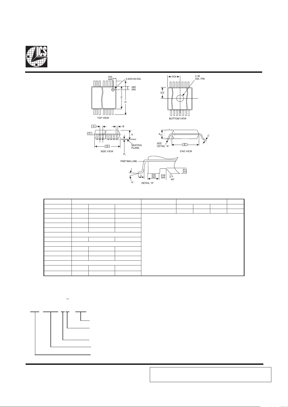
This table in inches
SSOP Package
LOBMYS SNOISNEMIDNOMMOC SNOITAIRAV D N
.NIM.MON.XAM.NIM.MON.XAM
A590.101.011.CA026.526.036.84
1A800.210.610.
2A880.090.290.
B800.010.5310.
C500.600.5800.
DsnoitairaVeeS
E292.692.992.
eCSB520.0
H004.604.014.
h010.310.610.
L420.230.040.
NsnoitairaVeeS
∝
°0°5°8
X580.390.001.
ICS reserves the right to make changes in the device data identified in this
publication without further notice. ICS advises its customers to obtain the latest
version of all device data to verify that any information being relied upon by the
customer is current and accurate.
Ordering Information
ICS9148yF-12
Pattern Number (2 or 3 digit number for parts with ROM code patterns)
Package Type
F=SSOP
Revision Designator (will not correlate with datasheet revision)
Device Type (consists of 3 or 4 digit numbers)
Prefix
ICS, AV = Standard Device
Example:
ICS XXXX y F - PPP
18
ICS9148-12
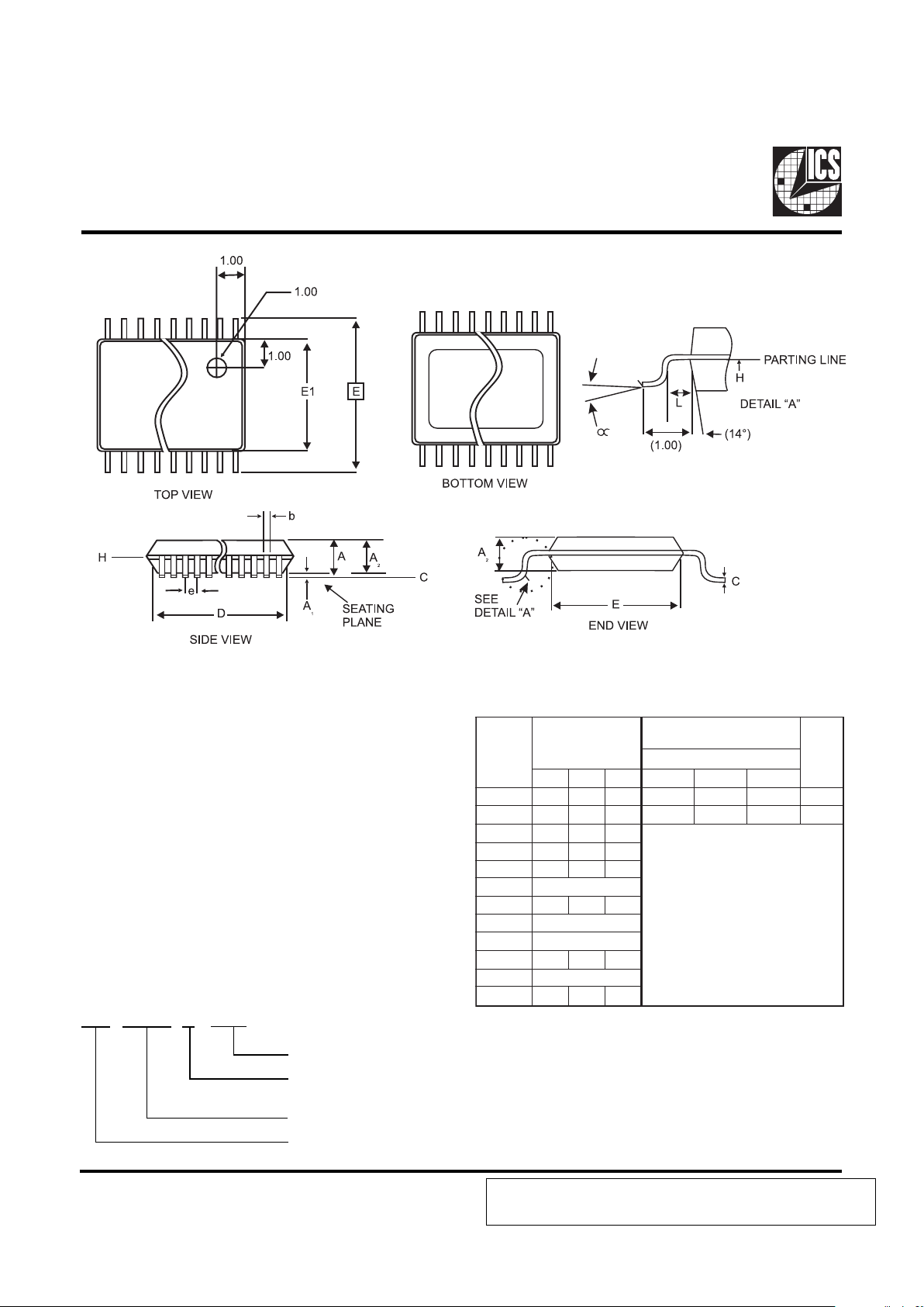
240 mil (6.10mm)TSSOP Package
Ordering Information
ICS9148G-12
ICS reserves the right to make changes in the device data identified in this
publication without further notice. ICS advises its customers to obtain the latest
version of all device data to verify that any information being relied upon by the
customer is current and accurate.
Diminisions are in millimeters
240TSSOP_AN
LOBMYS
NOMMOC
SNOISNEMID
SNOITAIRAV
N
D
.NIM.MON.XAM.NIM.MONXAM
A——01.104.2105.2106.2184
1A50.0—51.009.3100.4101.4165
2A58.009.059.0
b71.0—72.0
C90.0—02.0
DsnoitairaVeeS
1E00.601.602.6
eCSB05.0
ECSB01.8
L05.006.007.0
NsnoitairaVeeS
α
°0— °8
Pattern Number (2 or 3 digit number for parts with ROM code patterns)
Package Type
G=TSSOP
Device Type (consists of 3 or 4 digit numbers)
Prefix
ICS, AV = Standard Device
Example:
ICS XXXX G - PPP
 Loading...