ICST AV9147F-22 Datasheet

Integrated
Circuit
Systems, Inc.
General Description Features
ICS9147-22
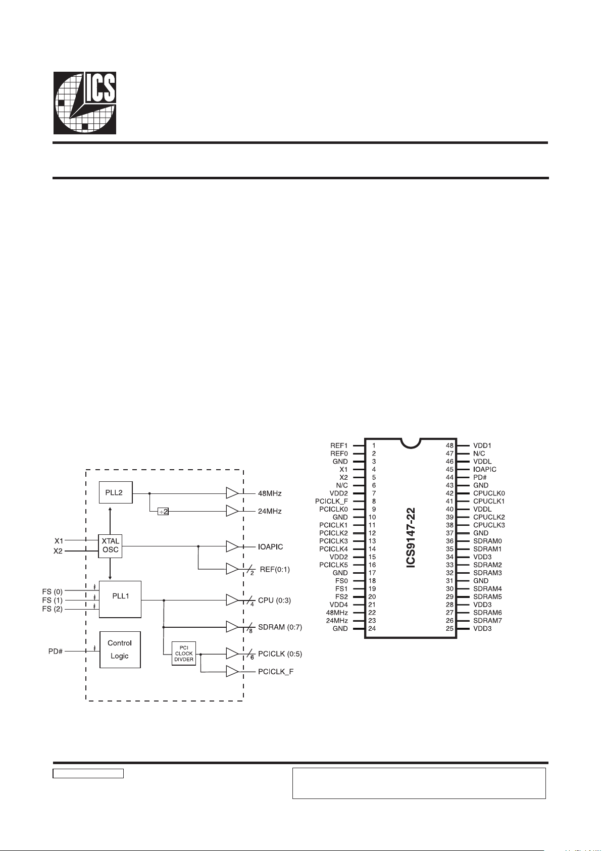
Block Diagram
Pentium/ProTM System and Cyrix Clock Chip
9147-22 Rev A 072597P
Pin Configuration
48-Pin SSOP
Pentium is a trademark on Intel Corporation.
Generates system clocks for CPU, IOAPIC, SDRAM,
PCI, plus 14.318 MHz (REF0:1), USB, Super I/O
Supports single or dual processor systems
Supports Intel 60, 66.8MHz, Cyrix 55, 75MHz plus 83.3
and 68MHz (Turbo of 66.6) speeds.
Synchronous clocks skew matched to 250ps window on
CPU, SDRAM and 500ps window on PCI clocks
CPU clocks to PCI clocks skew 1-4ns (CPU early)
Two fixed outputs, 48MHz and 24 MHz
Separate 2.5V and 3.3V supply pins
- 2.5V or 3.3V output: CPU, IOAPIC
- 3.3V outputs: SDRAM, PCI, REF, 48/24 MHz
No power supply sequence requirements
48 pin 300 mil SSOP
The ICS9147-22 is a Clock Synthesizer chip for Pentium
and PentiumPro plus Cyrix CPU based Desktop/Notebook
systems that will provide all necessary clock timing.
Features include four CPU, seven PCI and eight SDRAM
clocks. Two reference outputs are available equal to the
crystal frequency, plus the IOAPIC output powered by
VDDL. Additionally, the device meets the Pentium powerup stabilization, which requires that CPU and PCI clocks
be stable within 2ms after power-up.
High drive PCICLK and SDRAM outputs typically provide
greater than 1 V/ns slew rate into 30pF loads. CPUCLK
outputs typically provide better than 1V/ns slew rate into
20pF loads while maintaining 50 ±5% duty cycle. The REF
clock outputs typically provide better than 0.5V/ns slew
rates.
The ICS9147-22 accepts a 14.318MHz reference crystal
or clock as its input and runs on a 3.3V supply.
Power Groups
VDD1 = REF (0:1), X1, X2
VDD2 = PCICLK_F, PCICLK (0:5)
VDD3 = SDRAM (0:7),
VDD4 = 48MHz, 24MHz
VDDL = IOAPIC, CPUCLK (0:3)
ICS reserves the right to make changes in the device data identified in this
publication without further notice. ICS advises its customers to obtain the latest
version of all device data to verify that any information being relied upon by the
customer is current and accurate.

2
ICS9147-22
Pin Descriptions
PIN NUMBER PIN NAME TYPE DESCRIPTION
1 REF1 OUT Reference clock output
2 REF0 OUT Reference clock output
3, 10, 17, 24, 31,
31, 37, 43
GND PWR Ground (common)
4X1 IN
Crystal or refer ence input, no minally 14.3 18 MHz. Includes
internal load cap to GND an d feedback resistor from X2.
5 X2 OUT Crystal output, includes internal load cap to GND.
6, 47 N/C - Pins are not internally connected
7, 15 VDD2 PWR Supply for PCICLKF, and PCICLK (0:5)
8 PCICLK_F OUT Free running PCI clock
9, 11, 12, 13, 14, 16 PCICLK (0:5) OUT PCI clocks
18 FS0 IN Frequency sele ct 0 input
1
19 FS1 IN Frequency sele ct 1 input
1
20 FS2 IN Frequency sele ct 2 input
1
21 VDD4 PWR Supply for 48MHz and 24MHz clocks
22 48MHz OUT 48MHz driver output for USB clock
23 24MHz OUT 24MHz driver output for Super I/O clock
25, 28,34 VDD3 PWR Supply for SDRAM (0:7)
26, 27, 29, 30,
32, 33, 35, 36
SDRAM (0:7) OUT SDRAMs clock at CPU speed
38, 39, 41, 42 CPUCLK (0:3) OUT CPUCLK clock output, powered by VDDL
40, 46 VDDL PWR Supply for CPUCLK (0:3) + IOAPIC
44 PD# IN
Power down stops all clocks low and disab les oscillator and
internal VCO’s.
2
45 IOAPIC OUT IOAPIC clock output, powe red by VDDL at crystal frequency
48 VDD1 PWR Supply for REF (0:1), X1, X2
Note 1: Internal pull-up resistor of nomimally 100K to 120K at 3.3V on indicated inputs.
Note 2: The PD# input pin has a protection diode clamp to the VDDL power supply. If VDDL is not connected to VDD, (ie
VDDL=2.5V, VDD=3.3V) then this input must have a series resistor if the logic high is connected to VDD. This input
series resistor provides current limit for the clamp diode. For a pullup to VDD it should be 1Kohm or more from the PD#
pin to VDD. If the PD# pin is being driven by logic powered by 3.3V, then a 100Ω series resistor will be suffcient.

3
ICS9147-22
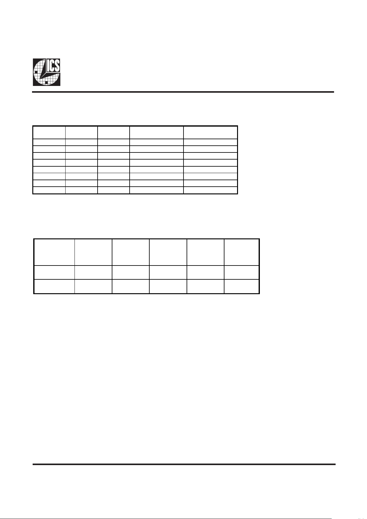
Functionality
VDD = 3.3V ±5% V
DDL
= 2.5V ±5% or 3.3V ±5%, TA = 0 to 70°
Crystal (X1, X2) = 14.31818 MHz
Power Management Functionality
FS2 FS1 FS0
CPUCLK, SDRAM
(MHz)
PCICLK
(MHz)
0 0 0 8.33 1/2 CPU
0 0 1 75 30
0 1 0 83.3 33.3
0 1 1 68.5 1/2 CPU
1 0 0 55 1/2 CPU
1 0 1 75 1/2 CPU
1 1 0 60 1/2 CPU
1 1 1 66.8 1/2 CPU
PD#
CPUCLK
Outputs
PCICLK(0:5)
Outputs
PCICLK_ F,
REF,
24/48MHz
and SDRAM
Crystal
OSC
VCO
0 Stopped Low Stopped Low Stopped Low Off Off
1 Running Running Running Running Running
 Loading...