ICST AV9120M-48, ICS9120M-48 Datasheet

Integrated
Circuit
Systems, Inc.
General Description
Features
ICS9120-48
Frequency Generator for CD-ROM Systems
9120-48 Rev A110196
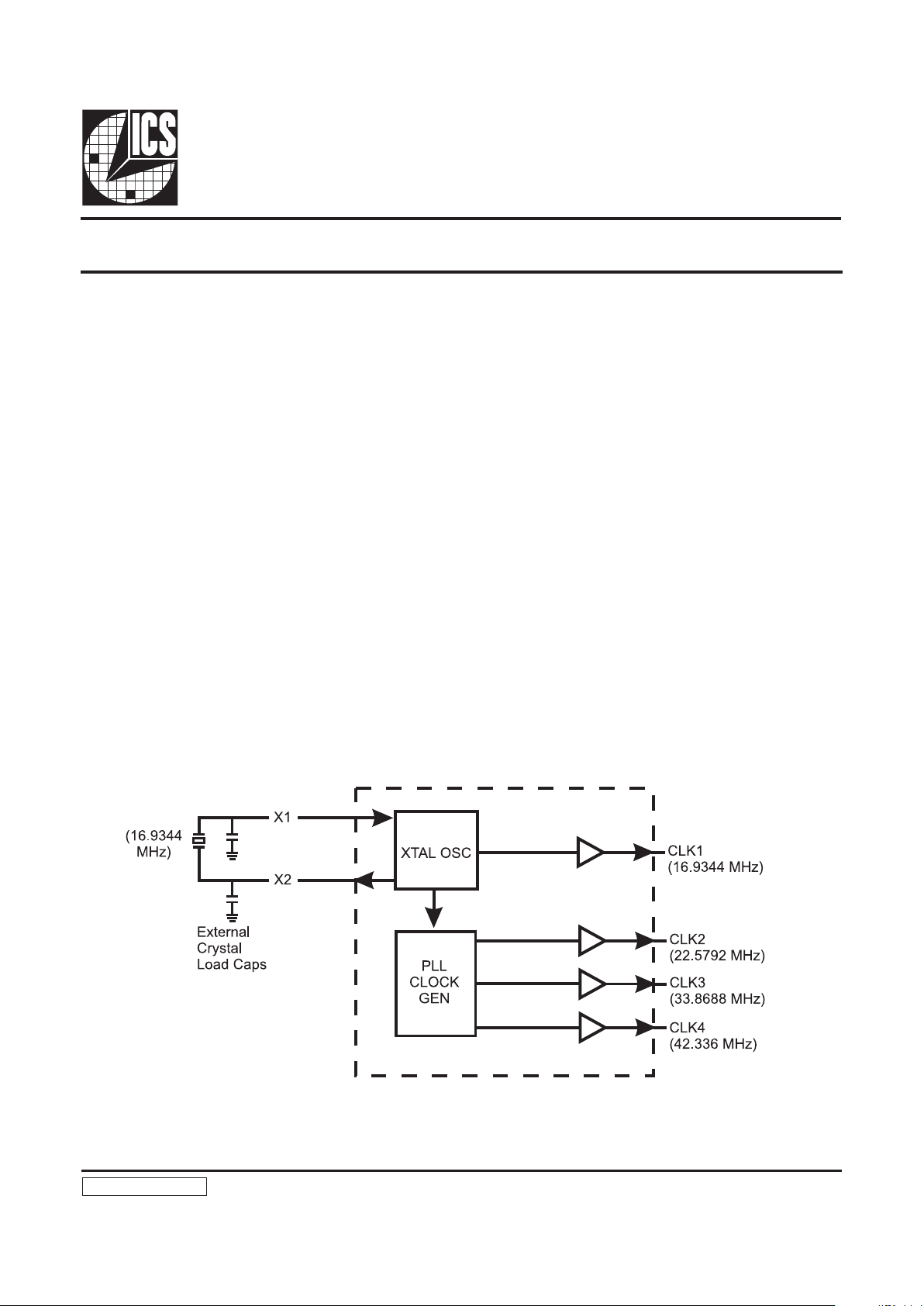
Block Diagram
The ICS9120-48 is a high performance frequency generator
designed to support digital compact disk drive systems. It
offers all clock frequencies required for the servo and decoder
sections of these devices. These frequencies are synthesized
from a single 16.9344 MHz on-chip oscillator.
High accuracy, low jitter PLLs meet the 150 ppm frequency
tolerance required by these systems. Fast output clock edge
rates minimize board induced jitter.
Unlike competitive devices, the ICS9120-48 operates over
the entire 3.0-5.5V range.
Generates the output clock frequencies required by
CD-ROM drive systems
Single 16.9344 MHz crystal or system clock reference
100ps one sigma jitter
Output rise/fall times less than 2.0ns (at 5V VDD)
On-chip loop filter components
3.0V-5.5V supply range
150 ppm output frequency accuracy
8-pin, 150-mil SOIC
Applications
Specifically designed to support CD-ROM drive
requirements of multimedia applications

2
ICS9120-48
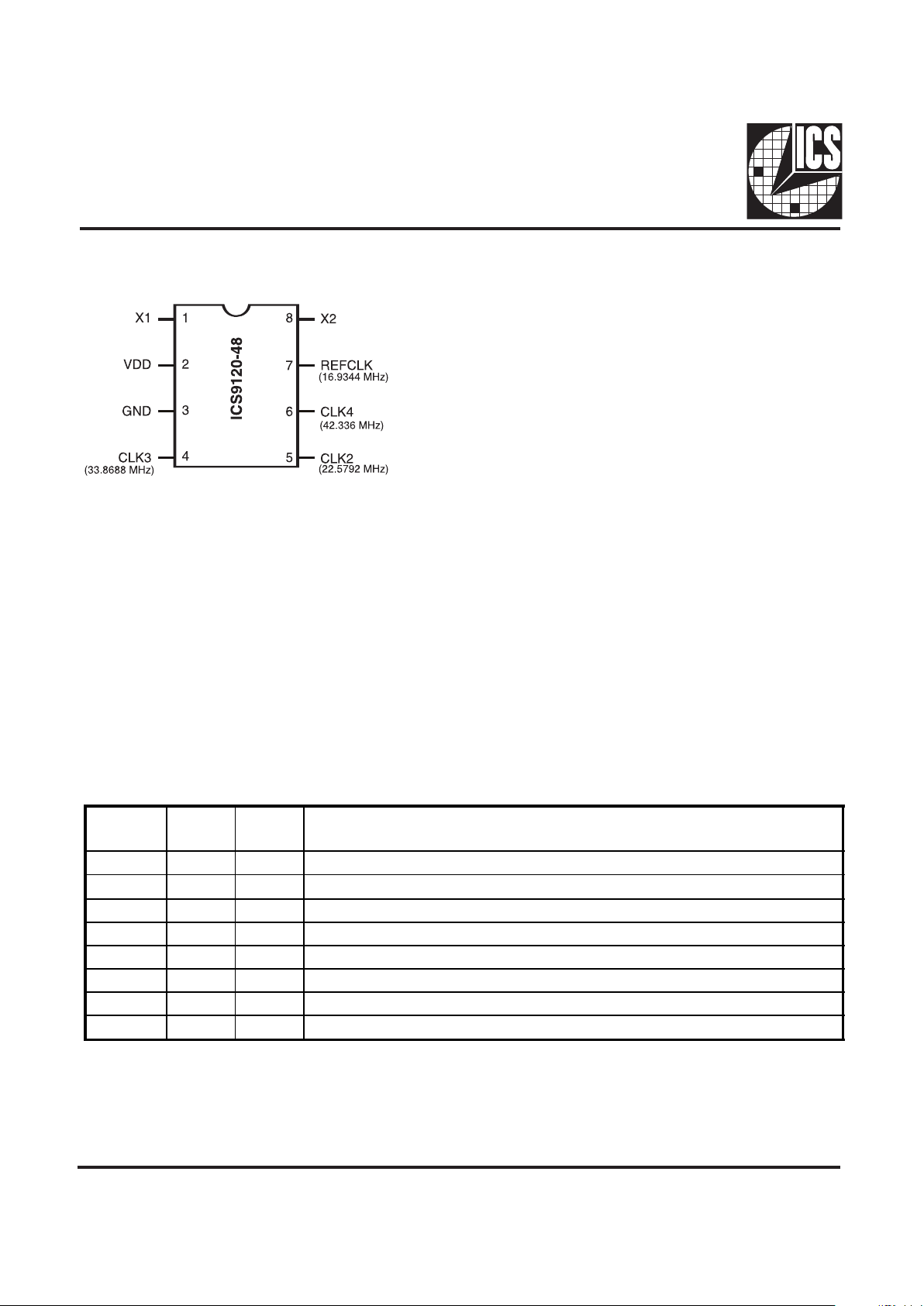
Pin Configuration
Pin Descriptions for ICS9120-48
8-Pin SOIC
External Components/Crystal Selection
The ICS9120-48 incorporates a crystal oscillator circuit de-signed
to provide 50% duty cycle over a range of operating conditions,
including the addition of external crystal load ca-pacitors to pins
X1 and X2. A parallel resonant 16.9344 MHz, 12pF load crystal is
recommended. A series resonant crystal or a parallel resonant
crystal specifying a different load can be used, but either will
result in frequencies which are slightly (up to 0.06%) different
from the ideal.
The crystal load capacitance can be increased by adding a capacitor
to each of the X1 and X2 pins and ground. This enables the use of
a crystal specifying a load greater than 12pF without changing the
output frequency.
Duty cycle is also maintained when using an external clock source
(connected to X1, X2 left unconnected) as long as the external
clock has good duty cycle.
PIN
NUMBE R
PIN
NAME
TYPE DESCRIPTION
1 X1 Input Crystal or external clock source. Has feedback bias for crystal.
2 VDD Power +Power supply input.
3 GND Power Ground return for Pin 2.
4 CLK3 Output 33.8688 MHz target output clock.
5 CLK2 Output 22.5792 MHz target output clock.
6 CLK4 Output 42.336 MHz target output clock.
7 CLK1 Output 16.9344 MHz reference clock buffered output.
8 X2 Output Crystal output drive (leave this pin unconnected when using an external clock).
 Loading...