ICST AV9120M-11, ICS9120M-11 Datasheet

Integrated
Circuit
Systems, Inc.
General Description
Features
ICS9120-11
The ICS9120-11 is a high performance frequency generator.
The ICS9120-11 provides high accuracy; low jitter PLLs
meet the 0.20% frequency tolerance and -96dB signal-tonoise ratios. Fast output clock edge rates minimize board
induced jitter.
The ICS9120-11 operates over the entire 3.0 - 5.5V range
and provides power-down to minimize energy consumption.
• Generates 46.6 MHz and 33.868 MHz clocks
• Buffered REFCLK output
• 0.20% frequency accuracy
• 100ps one sigma jitter maintains 16-bit performance
• Output rise/fall times less than 2.5ns
• On-chip loop filter components
• 3.0V - 5.5V supply range
• 8-pin, 150-mil SOIC package Advance Information
9120-11 Rev B 012197
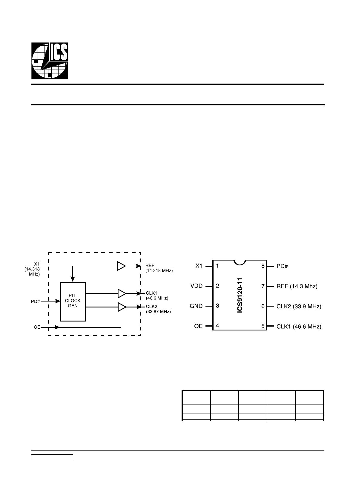
Block Diagram
Frequency Generator for Multimedia Audio Synthesis
X1 (MHz) PD#
33.9
(MHz)
46.6
(MHz)
14.3
(MHz)
- 0 Low Low Low
14.318 1 33.868 46.6 14.318
Functionality
Note: PD# (Pin 8) and OE (Pin 4) are internally pulled-up
to VDD and therefore may be left disconnected or driven by
open collector logic.
Pin Configuration
8-Pin SOIC

2
ICS9120-11
Pin Descriptions for ICS9120-11
* Pin 1 contains no loading capacitor.
PIN
NUMBER
PIN
NAME
TYPE DESCRIPTION
1 X1 Input External clock source.*
2 VDD Power +Power supply input.
3 GND Power Ground return for Pin 2.
4 OE Input Output Enable (tristates all outputs when at logic low level); has pull-up.
5 CLK1 Input 46.6 MHz clock output.
6 CLK2 Output 33.9 MHz clock output.
7 REF Output 14.318 M Hz reference clock output.
8 PD# Input Power-down input (powers-down entire device when low); has pull-up.
 Loading...