ICST AV9117M-01, ICS9117M-01 Datasheet

Integrated
Circuit
Systems, Inc.
General Description
Features
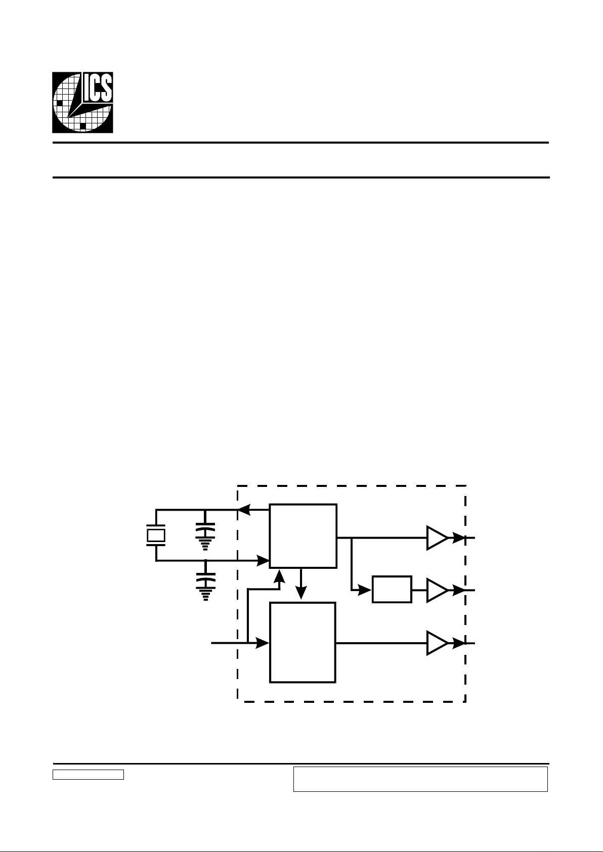
XTAL
OSC
PCLK
UCLK
MCLK
PLL
CLOCK
GEN
÷8
X2
14.7456
MHz
X1
PD
•
Generates the 14.7456 MHz microcontroller, 40.320
MHz datadump and 1.84320 UART clocks
• Less than ±80 ppm frequency variation including
temperature, voltage, load and aging tolerances
• Single crystal reference minimizes crystal reliability
and inventory issues
• 80 ps one sigma jitter maintains 16-bit performance
• Output rise/fall times less than 1.5 ns
• On-chip loop filter components
• 3.0 V - 5.5 V supply range
• 8-pin, 150-mil SOIC package
Applications
• Specifically designed to support the high performance
of fax/data modems
9117-01 RevA 052297P
Pentium is a trademark of Intel Corporation
PowerPC is a trademark of Motorola Corporation
Frequency Generator for Modem Systems
ICS9117-01
The ICS9117-01 is a low-cost, high-performance frequency
generator designed to support fax/data modem systems.
Datapump and UART clocks are synthesized from a
microcontroller crystal using high-accuracy, low-jitter PLLs,
meeting the frequency tolerance and -96dB signal-to-noise
ratios required by 16-bit DSP modem systems. Fast output
clock edge rates minimize boar d induced jitter.
Exact frequency multiplying ratios ensure better than ±80
ppm frequency accuracy using a standard AT crystal with
external load capacitors (typically 33pF ±5% for an 18pF
series load crystal). Achieving ±80ppm over four years
requires the crystal to have 20 ppm initial accuracy , ±20 ppm
temperature and ±5 ppm/year aging coefficients.
Block Diagram
PRODUCT PREVIEW documents contain information on products in the formative or
design phase development. Charactersitic data and other specifications are design
goals. ICS reserves the right to change or discontinue these procucts without notice.

2
ICS9117-01
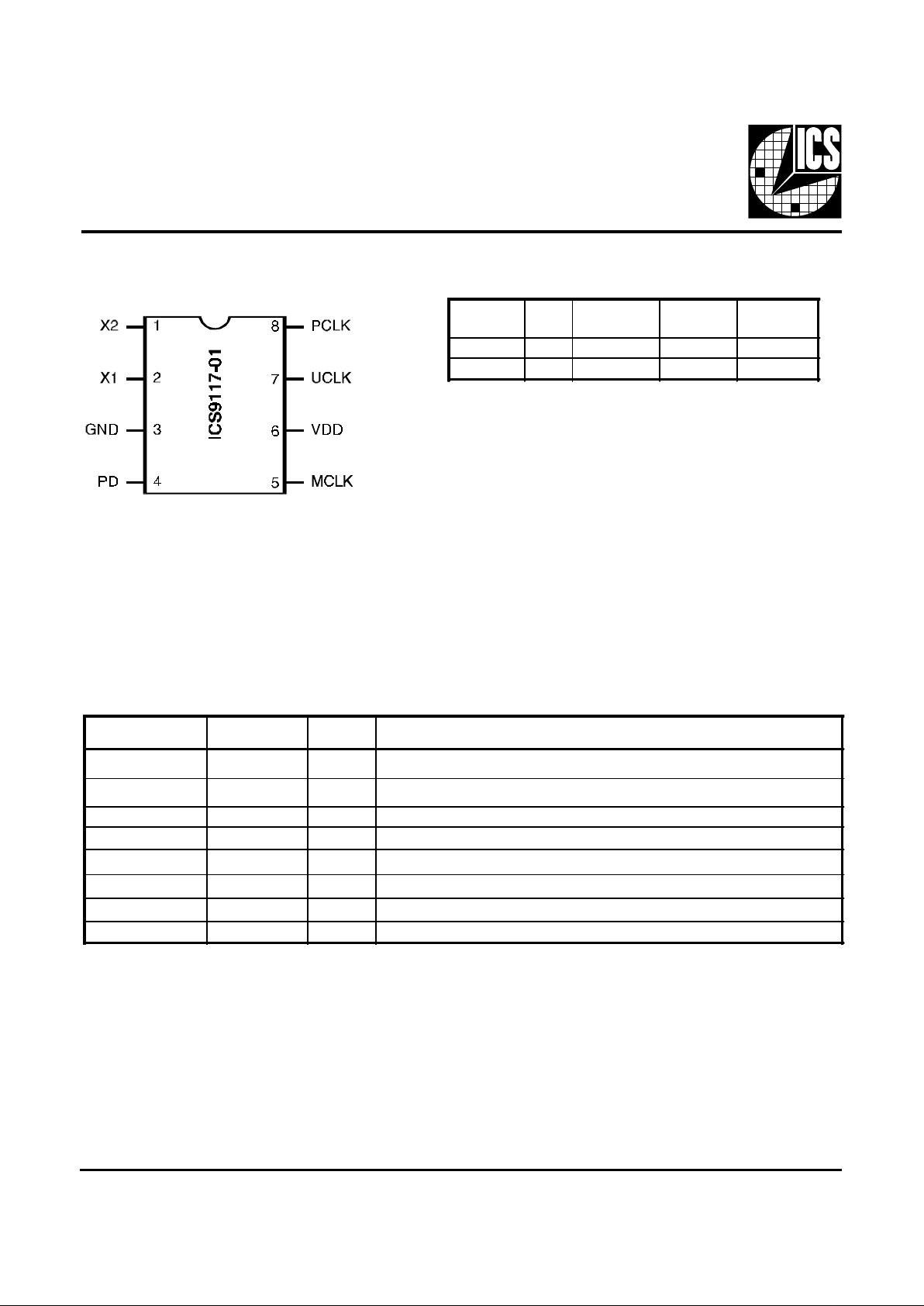
Pin Configuration
Pin Descriptions
Functionality
X1, X2
(MHz)
PD PCLK
(MHz)
MCL K
(MHz)
UCLK
(MHz)
14.7456 0 14.7456 40.320 1.8432
14. 7 45 6 1 L ow Low Low
PIN NU MBE R PIN NA ME TYP E DES CRI PT ION
1 X2 OUT Drive to crystal.
2 X1 IN Crystal or clock input.
3 GND PWR P ower s upp ly gr ound .
4 PD IN Power-down signal. Power-down all loops and oscilla tors.
5 MCLK OUT Dat ap ump 40 .32 MHz cl ock outp ut.
6 VDD PWR + 5V powe rs upp ly
7 UCLK OUT UART 1.84 MHz data cloc k output.
8 PCLK OUT Microcontroller 14.7 MHz clock output.
8-PIN SOIC
 Loading...