Integrated
Circuit
Systems, Inc.
General Description Features
ICS9112-16
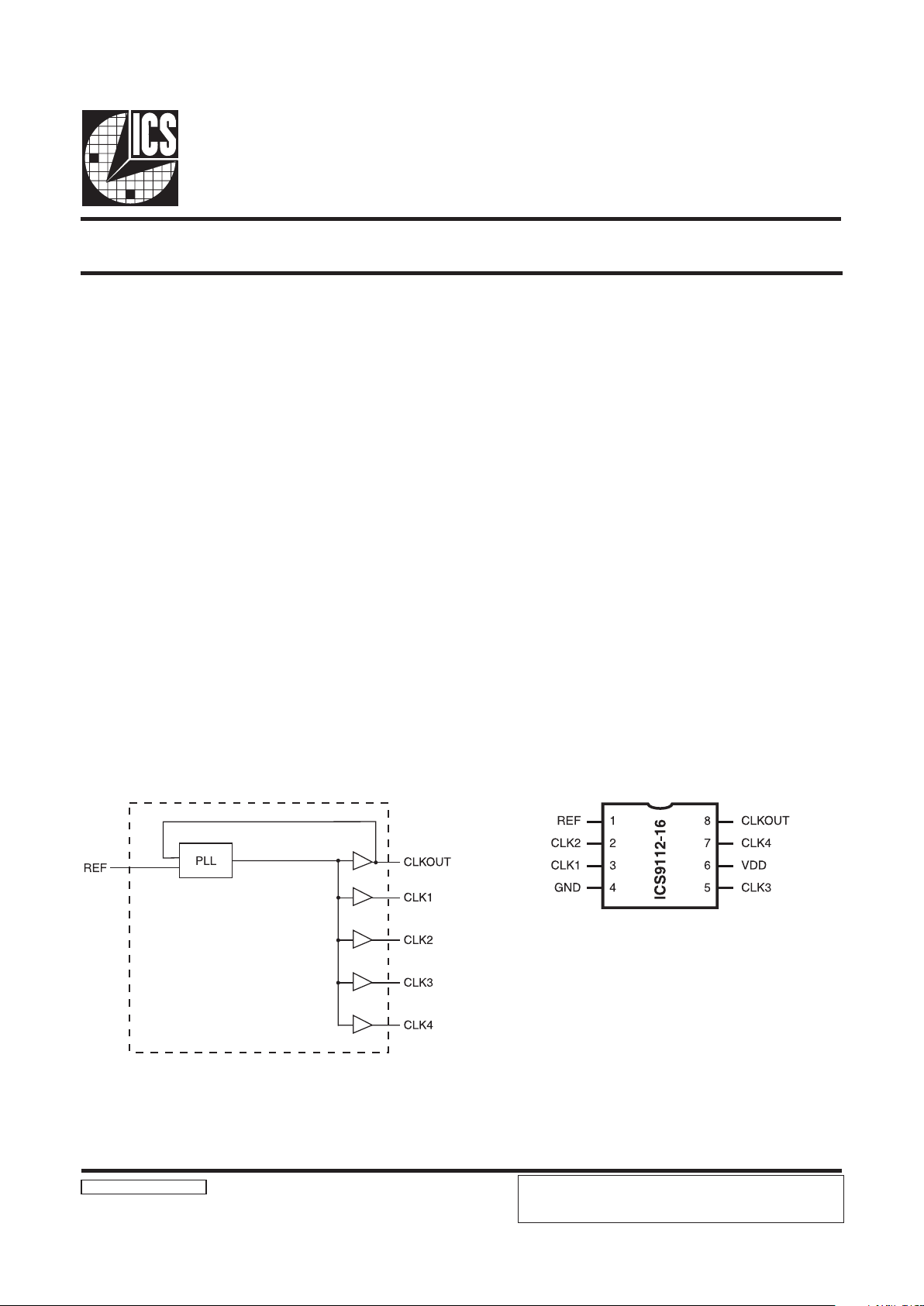
Block Diagram
Low Skew Output Buffer
9112-16 Rev F 10/20/00
Pin Configuration
• Zero input - output delay
• Frequency range 25 - 133 MHz (3.3V)
• High loop filter bandwidth ideal for Spread
Spectrum applications.
• Less than 200 ps Jitter between outputs
• Skew controlled outputs
• Skew less than 250 ps between outputs
• Available in 8 pin 150 mil SOIC
or 173 mil TSSOP package.
• 3.3V ±10% operation
The ICS9112-16 is a high performance, low skew, low jitter
clock driver. It uses a phase lock loop (PLL) technology to
align, in both phase and frequency, the REF input with the
CLKOUT signal. It is designed to distribute high speed
clocks in PC systems operating at speeds from 25 to
133 MHz.
ICS9112-16 is a zero delay buffer that provides
synchronization between the input and output. The
synchronization is established via CLKOUT feed back to the
input of the PLL. Since the skew between the input and
output is less than +/- 350 pS, the part acts as a zero delay
buffer.
The ICS9112-16 comes in an eight pin 150 mil SOIC or 173
mil TSSOP package. It has five output clocks. In the absence
of REF input, will be in the power down mode. In this mode,
the PLL is turned off and the output buffers are pulled low.
Power down mode provides the lowest power consumption
for a standby condition.
8 pin SOIC, TSSOP
ICS reserves the right to make changes in the device data identified in
this publication without further notice. ICS advises its customers to
obtain the latest version of all device data to verify that any
information being relied upon by the customer is current and accurate.

2
ICS9112-16
Pin Descriptions
Notes:
1. Guaranteed by design and characterization. Not subject to 100% test.
2. Weak pull-down
3. Weak pull-down on all outputs
REBMUNNIPEMANNIPEPYTNOITPIRCSED
1FER
2
NI.ycneuqerfecnerefertupnI
22KLC
3
TUOtuptuokcolcdereffuB
31KLC
3
TUOtuptuokcolcdereffuB
4DNGRWPdnuorG
53KLC
3
TUOtuptuokcolcdereffuB
6DDVRWP)V3.3(ylppuSrewoP
74KLC
3
TUOtuptuokcolcdereffuB
8TUOKLC
3
TUOnipsihtnokcabdeeflanretnI.tuptuokcolcdereffuB

3
ICS9112-16
Notes:
1. Guaranteed by design and characterization. Not subject to 100% test.
2. All Skew specifications are mesured with a 50W transmission line, load teminated with 50W to 1.4V.
3. Duty cycle measured at 1.4V.
4. Skew measured at 1.4V on rising edges. Loading must be equal on outputs.
Absolute Maximum Ratings
Supply Voltage . . . . . . . . . . . . . . . . . . . . . . . . . . 7.0 V
Logic Inputs . . . . . . . . . . . . . . . . . . . . . . . . . . . . GND –0.5 V to VDD +0.5 V
Ambient Operating Temperature . . . . . . . . . . 0°C to +70°C
Storage Temperature. . . . . . . . . . . . . . . . . . . . . –65°C to +150°C
Electrical Characteristics at 3.3V
VDD = 3.0 – 3.6 V, TA = 0 – 70° C unless otherwise stated
Stresses above those listed under Absolute Maximum Ratings may cause permanent damage to the device. These ratings
are stress specifications only and functional operation of the device at these or any other conditions above those listed
in the operational sections of the specifications is not implied. Exposure to absolute maximum rating conditions for
extended periods may affect product reliability.
scitsiretcarahCCD
RETEMARAPLOBMYSSNOITIDNOCTSETNIMPYTXAMSTINU
egatloVwoLtupnI
V
LI
8.0V
egatloVhgiHtupnI
V
HI
0.2V
tnerruCwoLtupnI
I
LI
VNIV0=910.05Aµ
tnerruChgiHtupnI
I
HI
VNIV=
DD
01.00.001Aµ
egatloVwoLtuptuO
1
V
LO
I
LO
Am52=52.04.0V
egatloVhgiHtuptuO
1
V
HO
I
HO
Am52=4.29.2V
ylppuSnwoDrewoP
tnerruC
I
DD
zHM0=FER3.00.05Aµ
tnerruCylppuS
I
DD
LESzHM66.66tastutuodedaolnU
Vtastupni
DD
DNGro
0.030.04Am
 Loading...