

Integrated
Circuit
Systems, Inc.
General Description Features
ICS91 12-17
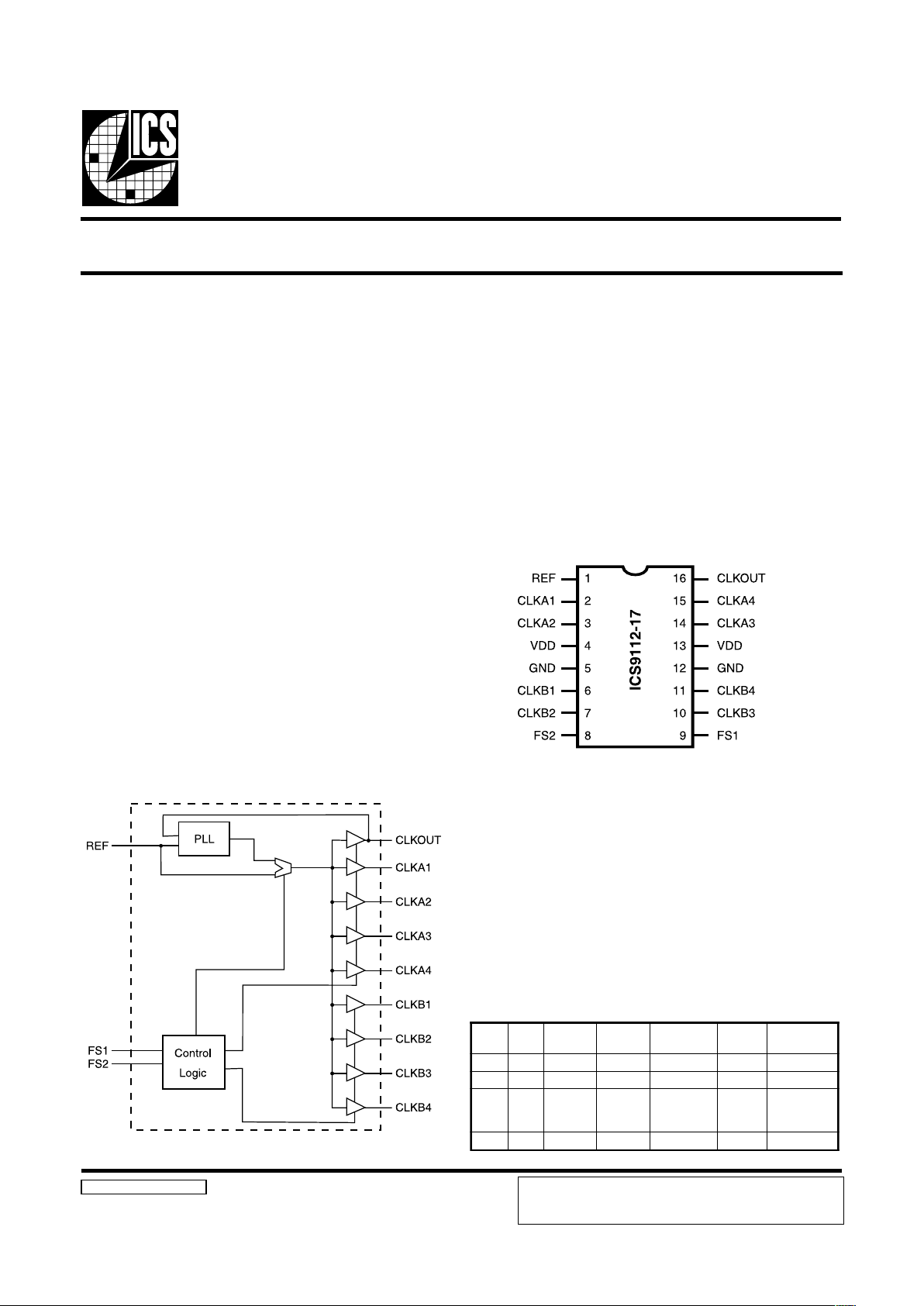
Block Diagram
Low Skew Output Buffer
9112-17 Rev G 10/20/00
Pin Configuration
• Zero input - output delay
• Frequency range 25 - 133 MHz (3.3V)
• High loop filter bandwidth ideal for Spread Spectrum
applications.
• Less than 200 ps cycle to cycle Jitter
• Skew controlled outputs
• Skew less than 250 ps between outputs
• Available in 16 pin, 150 mil SSOP & SOIC package
The ICS9112-17 is a high performance, low skew, low jitter
zero delay buffer . It uses a phase lock loop (PLL) technology
to align, in both phase and frequency, the REF input with the
CLKOUT signal. It is designed to distribute high speed
clocks in PC systems operating at speeds from 25 to
133 MHz.
ICS9112-17 is a zero delay buffer that provides
synchronization between the input and output. The
synchronization is established via CLKOUT feed back to the
input of the PLL. Since the skew between the input and
output is less than +/- 350 pS, the part acts as a zero delay
buffer.
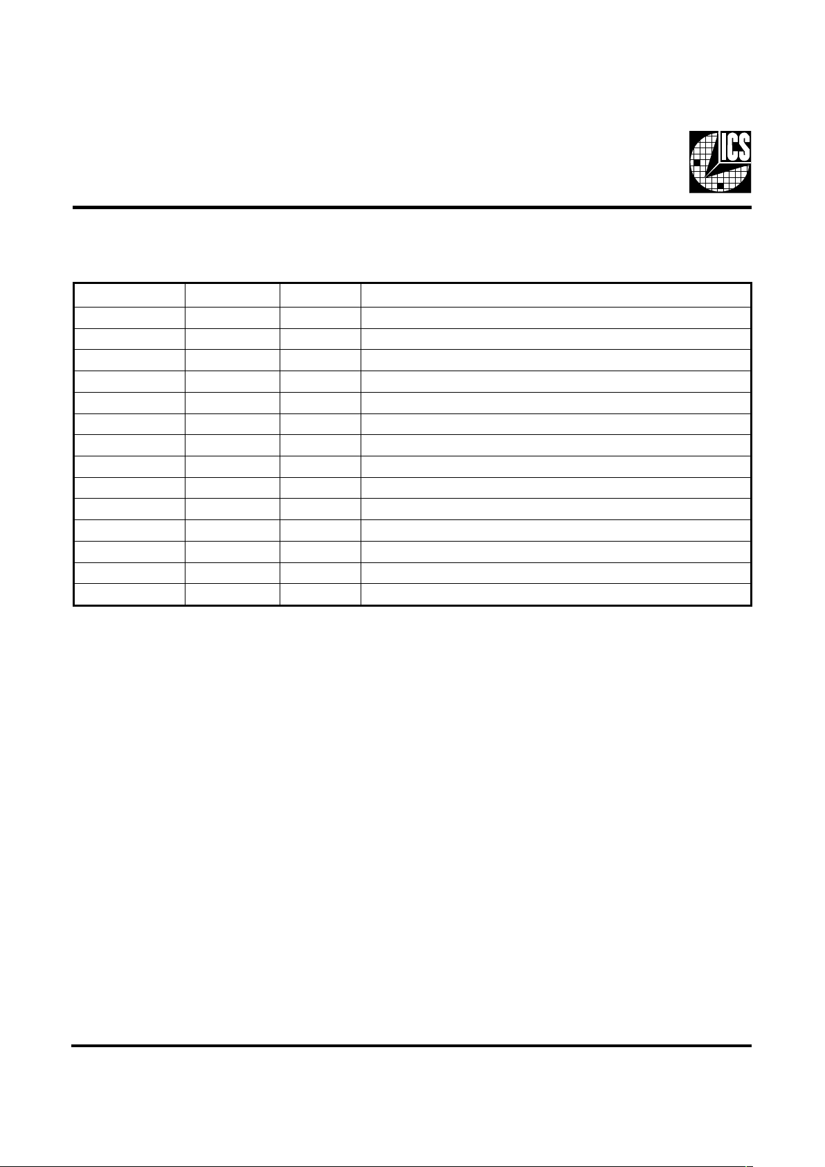
The ICS9112-17 has two banks of four outputs controlled by
two address lines. Depending on the selected address line,
bank B or both banks can be put in a tri-state mode. In this
mode, the PLL is still running and only the output buffers are
put in a high impedance mode. The test mode shuts off the
PLL and connects the input directly to the output buffers (see
table below for functionality).
The ICS9112-17 comes in a sixteen pin 150 mil SOIC or 16
pin SSOP package. In the absence of REF input, will be in the
power down mode. In this mode, the PLL is turned off and the
output buffers are pulled low. Power down mode provides
the lowest power consumption for a standby condition.
2SF1SF
AKLC
)4,1(
BKLC
)4,1(
TUOKLC
tuptuO
ecruoS
LLP
nwodtuhS
00 etatsirTetatsirTnevirDLLPN
01 nevirDetatsirTnevirDLLPN
10
LLP
ssapyB
edoM
LLP
ssapyB
edoM
LLP
ssapyB
edoM
FERY
11 nevirDnevirDnevirDLLPN
Functionality
ICS reserves the right to make changes in the device data identified in
this publication without further notice. ICS advises its customers to
obtain the latest version of all device data to verify that any
information being relied upon by the customer is current and accurate.
16 pin SSOP & SOIC
2
ICS9112-17
Pin Descriptions
Notes:
1. Guaranteed by design and characterization. Not subject to 100% test.
2. Weak pull-down
3. Weak pull-down on all outputs
4. Weak pull-ups on these inputs
REBMUNNIPEMANNIPEPYTNOITPIRCSED
1FER
2
NI.ycneuqerfecnerefertupnI
21AKLC
3
TUOAknaB,tuptuokcolcdereffuB
32AKLC
3
TUOAknaB,tuptuokcolcdereffuB
31,4DDVRWP)V3.3(ylppuSrewoP
21,5DNGRWPdnuorG
61BKLC
3
TUOBknaB.tuptuokcolcdereffuB
72BKLC
3
TUOBknaB.tuptuokcolcdereffuB
82SF
4
NI2tib,tupnitceleS
91SF
4
NI1tib,tupnitceleS
013BKLC
3
TUOBknaB.tuptuokcolcdereffuB
114BKLC
3
TUOBknaB.tuptuokcolcdereffuB
413AKLC
3
TUOAknaB,tuptuokcolcdereffuB
514AKLC
3
TUOAknaB,tuptuokcolcdereffuB
61TUOKLC
3
TUOnipsihtnokcabdeeflanretni,tuptuokcolcdereffuB
3
ICS9112-17
Absolute Maximum Ratings
Supply Voltage . . . . . . . . . . . . . . . . . . . . . . . . . . 7.0 V
Logic Inputs . . . . . . . . . . . . . . . . . . . . . . . . . . . . GND –0.5 V to VDD +0.5 V
Ambient Operating Temperature. . . . . . . . . . . . 0°C to +70°C
Storage Temperature . . . . . . . . . . . . . . . . . . . . . . –65°C to +150°C
Stresses above those listed under Absolute Maximum Ratings may cause permanent damage to the device. These ratings are
stress specifications only and functional operation of the device at these or any other conditions above those listed in the
operational sections of the specifications is not implied. Exposure to absolute maximum rating conditions for extended
periods may affect product reliability.
El e ctrical Characteristics - Input & Supply
TA = 0 - 70C; Supply Voltage VDD = 5.0 V +/-10% (unless othe rwis e stated)
PARAMETER SYMBOL CONDITIONS MIN TYP MAX UNITS
Input High Voltage V
IH
2.0 2.5 VDD +0.5 V
Input Low Voltage V
IL
GND -0.5 0.8 V
Input High Current I
I
H
V
I
N
= V
DD
0.1 100 uA
Input Low Current I
I
L
V
I
N
= 0 V; 19 50 uA
Operating current I
DD1
CL = 0 pF; F
I
N
@ 66M 45 65 mA
Input frequency F
i
1
VDD = 3.3 V ; All Output s Loade d 25 133 MHz
I nput Ca pa citance
C
IN
1
Logic Inputs 5 pF
1
Guarant eed by design, not 100% te sted in production.
Electrical Characteristics - Input & Supply
TA = 0 - 70C; Supply Voltage VDD = 3.3 V +/ -10% (unless otherwise state d)
PARAMETE R SYMBOL CONDITIONS M IN TYP MAX UNITS
Input High Voltage V
IH
2.0 2.0 VDD+0.3 V
Input Low Voltage V
IL
GND-0.3 0.8 V
Input High Curre nt I
I
H
V
I
N
= V
DD
0.1 100 uA
Input Low Current I
I
L
V
I
N
= 0 V; 19 50 uA
Operating current I
DD1
CL = 0 pF; F
I
N
@ 66M 30 45 mA
I nput f re quency F
i
1
VDD = 3.3 V; All Outputs Loaded 25 133 MHz
I nput Capacitance
C
IN
1
Logic Inputs 5.0 pF
1
Guarenteed by design, not 100% tested in production.

4
ICS9112-17
Electrical C haracteristics - OUTPUT
T
A
= 0 - 70C; V
DD
= V
DDL
= 3.3 V +/-10%; C
L
= 20 - 30 pF (unless otherwise stated)
PARAMETER SYMBOL CONDITIONS MIN TYP MAX UNITS
Output Impe dance R
DSP
VO = VDD*(0.5) 10 24 Ω
Output Impe dance R
DSN
VO = VDD*(0.5) 10 24 Ω
Output High Volta ge V
OH
IOH = -8 mA 2.4 2.9 5.0 V
Output Low Voltage V
OL
IOL = 8 mA 0.25 0.4 V
Rise Time
1
T
r
VOL = 0.8 V, VOH = 2.0 V 1.2 2.0 ns
Fall Time
1
T
f
VOH = 2.0 V, VOL = 0.8 V 1.2 2.0 ns
PLL Lock Time1 tLOCK
Stable power supply, valid cl ock presented on
REF pin
1.0 ms
D
t
VT = 1.4V;Cl=30pF 40 50 60 %
D
t
VT = Vdd/2; Fout <66.6MHz 45 50 55 %
Tcyc-cyc at 66MH z , Loaded O utputs 250 ps
Tcyc-cyc >66MHz , Loaded Outputs 200 ps
Absolute Jitter
1
Tjabs 10000 cycles; Cl=30pF -100 70 100 ps
Jitter; 1-Sigma
1
Tj1s 10000 cycles; Cl=30pF 14 30 ps
Skew
1
T
sk
VT = 1.4 V (Window) Output to Output 250 ps
Device to Device Skew
1
Tdsk-Tdsk
Measured at VDD/2 on the CLKOUT
pins of devices
0 700 ps
Delay Input-Output
1
D
R1
VT = 14 V
0 700 ps
1
Guaranteed by design, not 100% tested in production.
Cycle to Cycle jitter
1
Duty Cycle
1
Electrical Characteristics - OUTPUT
T
A
= 0 - 70C; V
DD
= V
DDL
= 5.0 V +/-10%; C
L
= 20 - 30 pF (unless otherwise stated)
PARAMETER SYMBOL CONDITIONS MIN TYP MAX UNITS
Output Impedance R
DSP
VO = VDD*(0.5) 10 24 Ω
Output Impedance R
DSN
VO = VDD*(0.5) 10 24 Ω
Output High Voltage V
OH
IOH = -8 mA 2.4 2.9 5.0 V
Output Low Voltage V
OL
IOL = 8 mA 0.25 0.4 V
Rise Time
1
T
r
VOL = 0.8 V, VOH = 2.0 V 0.8 1.5 ns
Fall Time
1
T
f
VOH = 2.0 V, VOL = 0.8 V 1.0 1.5 ns
PLL Lock Time
1
tLOCK
Stable power supply, valid c lock presented on
REF pin
1.0 ms
Duty Cycle
1
D
t
VT = 1.4V;Cl=30pF 40 50 60 %
Tcyc-cyc at 66MHz , Loaded Outputs 250 ps
Tcyc-cyc >66MHz , Loaded Outputs 200 ps
Absolute Jitter
1
Tjabs 10000 cycles; Cl=30pF -100 60 100 ps
Jitter; 1-Sigma
1
Tj1s 10000 cycles; Cl=30pF 14 30 ps
Skew
1
T
sk
VT = 1.4 V (Window) Output t o Output 250 ps
Device to Device Skew
1
Tdsk-Tdsk
Measured at VDD/2 on the CLKOUT
pins of devices
0 700 ps
Delay Input-Output
1
D
R1
VT = 14 V
0 700 ps
1
Guaranteed by design, not 100% tested in production.
Cycle to Cycle jitter
1

5
ICS9112-17
Output to Output Skew
The skew between CLKOUT and the CLKA/B outputs is not dynamically adjusted by the PLL. Since CLKOUT is one of the
inputs to the PLL, zero phase difference is maintained from REF to CLKOUT. If all outputs are equally loaded, zero phase
difference will maintained from REF to all outputs.
If applications requiring zero output-output skew, all the outputs must equally loaded.
If the CLKA/B outputs are less loaded than CLKOUT, CLKA/B outputs will lead it; and if the CLKA/B is more loaded than
CLKOUT , CLKA/B will lag the CLKOUT .
Since the CLKOUT and the CLKA/B outputs are identical, they all start at the same time, but different loads cause them to
have different rise times and different times crossing the measurement thresholds.
REF input and
all outputs
loaded
Equally
REF input and CLKA/B
outputs loaded equally, with
CLKOUT loaded More.
REF input and CLKA/B
outputs loaded equally, with
CLKOUT loaded Less.
Timing diagrams with different loading configurations

6
ICS9112-17
Application Suggestion:
ICS9112-17 is a mixed analog/digital product. The analog portion of the PLL is very sensitive to any random noise generated
by charging or discharging of internal or external capacitor on the power supply pins. This type of noise will cause excess
jitter to the outputs of ICS9112-17. Below is a recommended lay out to alleviate any addition noise. For additional
information on FT . layout, please refer to our AN07. The 0.1 uF capacitors should be connected as close as possible to power
pins (4 & 13). An Isolated power plane with a 2.2 uF capacitor to ground will enhance the power line stability.
33Ω
33Ω
33Ω
33Ω
10KΩ
0.1µF
VDD
GND
33Ω
33Ω
33Ω
33Ω
33Ω
10KΩ
0.1µF
VDD
GND
1
2
3
4
5
6
7
8
16
15
14
13
12
11
10
9
REF
CLKA1
CLKA2
VDD
GND
CLKB1
CLKB2
FS2
CLKOUT
CLKA4
CLKA3
VDD
GND
CLKB4
CLKB3
FS1

7
ICS9112-17
ICS reserves the right to make changes in the device data identified in
this publication without further notice. ICS advises its customers to
obtain the latest version of all device data to verify that any
information being relied upon by the customer is current and accurate.
Ordering Information
ICS9112yF-17-T
Designation for tape and reel packaging
Pattern Number (2 or 3 digit number for parts with ROM code patterns)
Package T ype
F=SSOP
Revision Designator (will not correlate with datasheet revision)
Device Type (consists of 3 or 4 digit numbers)
Prefix
ICS, AV = Standard Device
Example:
ICS XXXX y F - PPP - T

8
ICS9112-17
ICS reserves the right to make changes in the device data identified in
this publication without further notice. ICS advises its customers to
obtain the latest version of all device data to verify that any
information being relied upon by the customer is current and accurate.
ICS XXXX y M - PPP - T
Ordering Information
ICS9112yM-17-T
Designation for tape and reel packaging
Pattern Number (2 or 3 digit number for parts with ROM code patterns)
Package Type
M=SOIC
Revision Designator (will not correlate with datasheet revision)
Device Type (consists of 3 or 4 digit numbers)
Prefix
ICS, AV = Standard Device
Example:
 Loading...