ICST AV9110-02CS14, AV9110-02CN14, AV9110-01CS14, AV9110-01CN14, ICS9110-01CN14 Datasheet
...
Integrated
Circuit
Systems, Inc.
General Description Features
AV9110
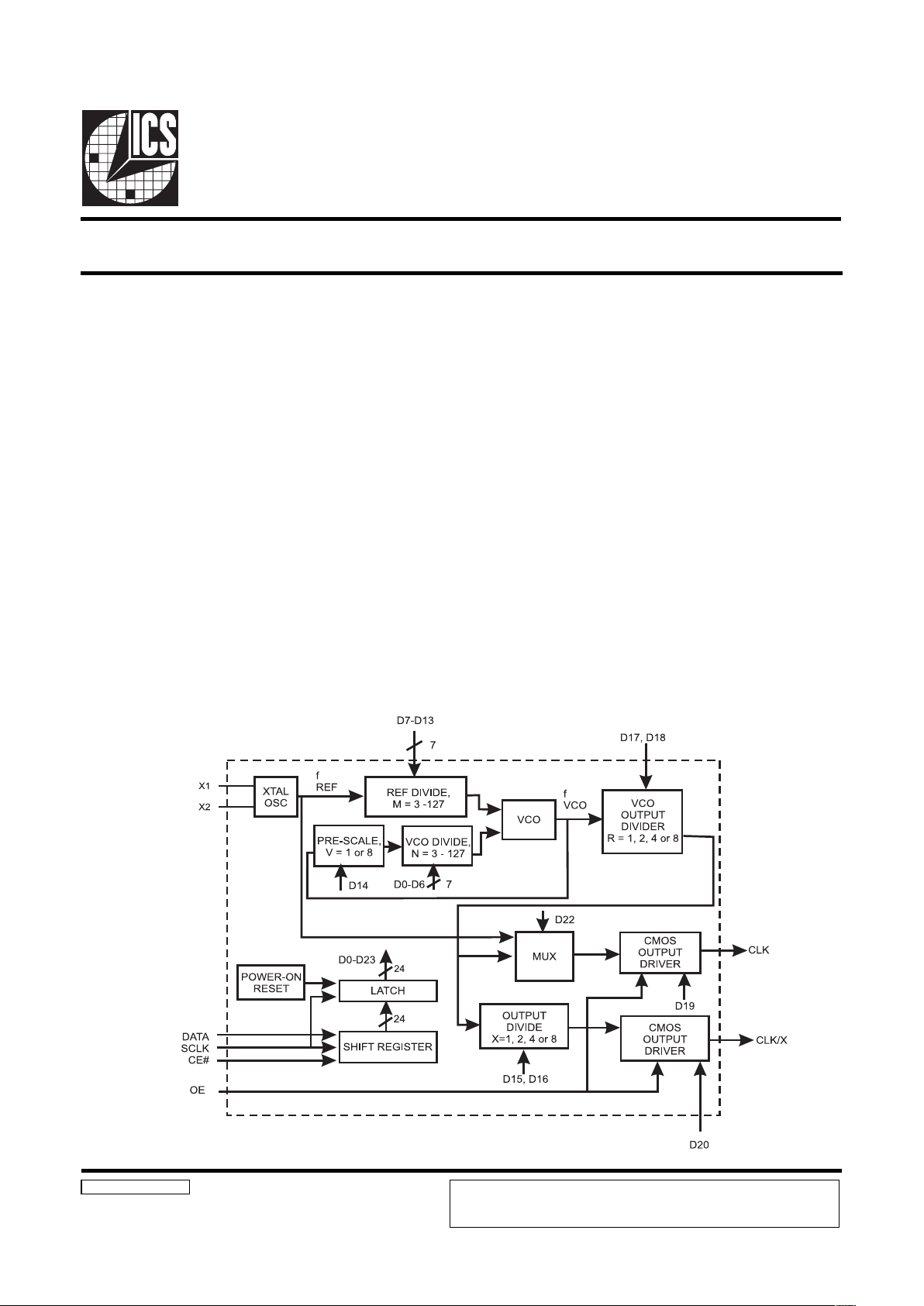
Block Diagram
Serially Programmable Frequency Generator
9110 Rev F 5/30/00
• Complete user programmability of output frequency
through serial input data port
• On-chip Phase-Locked Loop for clock generation
• Generates accurate frequencies up to 130 MHz
• Tristate CMOS outputs
• 5 volt power supply
• Low power CMOS technology
• 14-pin DIP or 150-mil SOIC
• Very low jitter
• Wide operating range V CO
The AV9110 generates user specified clock frequencies using
an externally generated input reference, such as 14.318 MHz
or 10.00 MHz crystal connected between pins 1 and 14.
Alternately, a TTL input reference clock signal can be used.
The output frequency is determined by a 24-bit digital word
entered through the serial port. The serial port enables the
user to change the output frequency on-the-fly.
The clock outputs utilize CMOS level output buffers that
operate up to 130 MHz.
Applications
Graphics: The AV9110 generates low jitter, high speed pixel
(or dot) clocks. It can be used to replace multiple expensive
high speed crystal oscillators. The flexibility of this device
allows it to generate nonstandard graphics clocks, allowing
the user to program frequencies on-the-fly.
ICS reserves the right to make changes in the device data identified in this
publication without further notice. ICS advises its customers to obtain the latest
version of all device data to verify that any information being relied upon by the
customer is current and accurate.

2
AV9110
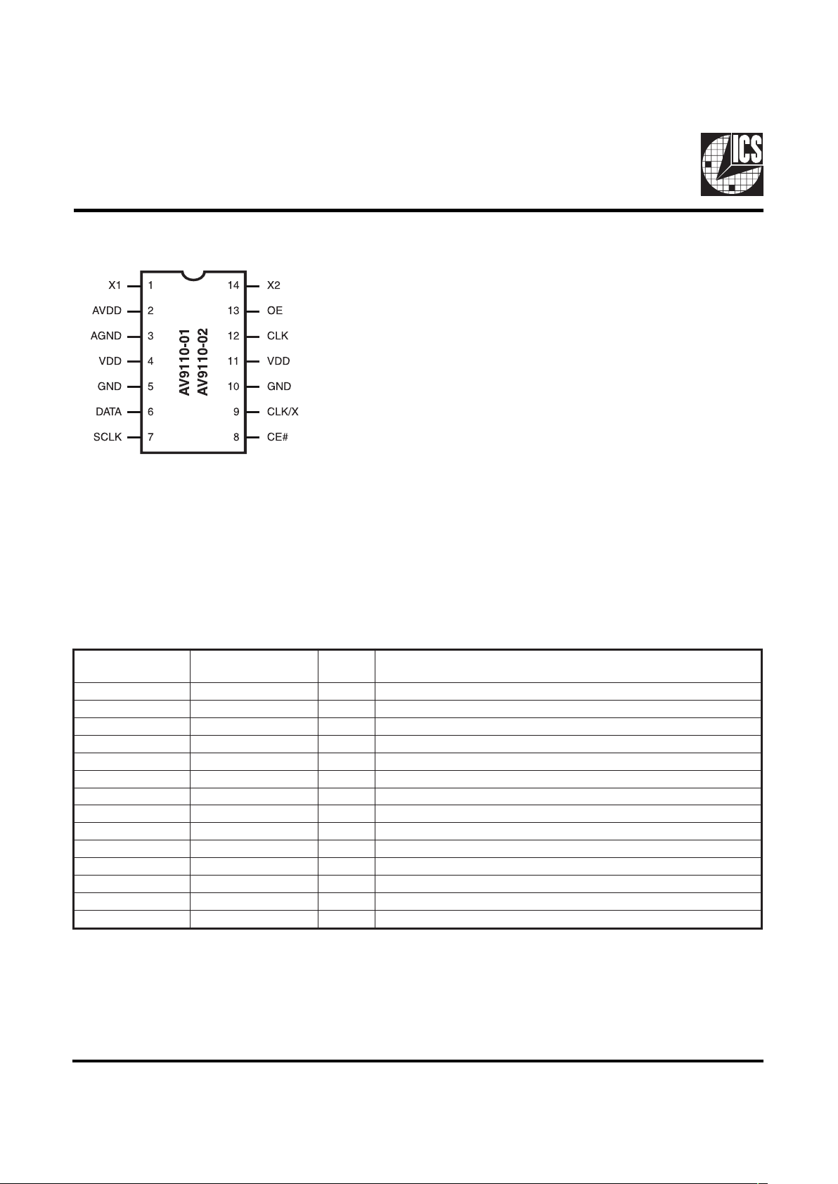
Pin Descriptions
Pin Configuration
14 Pin Dip, SOIC
The AV9110 requires a stable reference clock (5 to 32 MHz) to
generate a stable, low jitter output clock. The AV9 11 0 -01 is
optimized to use an external quartz crystal as a frequency
reference, without the need of additional external components.
The AV9110-02 is optimized to accept an TTL clock
reference. Either device can be used with an external crystal
or accept a TTL clock reference, although extra components
may be required. The various combinations implied are
summarized in Figure 2 (see page 7).
Clock Reference Implementations:
AV9110-01 vs. AV9110-02
REBMUNNIP EMANNIP
NIP
EPYT
NOITPIRCSED
11XtupnI.kcolcecnereferLTTrotupnilatsyrC
2DDVArewoP.V5+ottcennoC.ylppusrewopGOLANA
3DNGArewoP.DNUORGGOLANA
4DDVrewoP.V5+ottcennoC.ylppusrewoplatigiD
5DNGrewoP.DNUORGlatigiD
6ATADtupnI.nipATADlaireS
7KLCStupnI.retsigertfihsskcolC.KCOLCLAIRES
8#ECtupnI.refsnartatadslortnoc,wolevitcA.ELBANEPIHC
9X/KLCtuptuO.tuptuoXybdedividKCOLCSOMC
01DNGrewoP.DNUORGlatigiD
11DDVrewoP.V5+ottcennoC.ylppusrewoplatigiD
21KLCtuptuO.tuptuoKCOLCSOMC
31EOtupnI.wolnehwstuptuohtobsetatsirT.ELBANETUPTUO
412XtuptuO.kcolcecnereferLTTrotupnilatsyrC

3
AV9110
Electrical Characteristics
VDD = +5V±10%, TA = 0 – 70°C unless otherwise stated
Note 1: Parameter is guaranteed by design and characterization. Not 100% tested in production.
Absolute Maximum Ratings
Supply Voltage . . . . . . . . . . . . . . . . . . . . . . . . . . 7.0 V
Voltage on I/O pins referenced to GND . . . . . . GND –0.5 V to VDD +0.5 V
Operating Temperature under bias . . . . . . . . . . 0°C to +70°C
Power dissipation . . . . . . . . . . . . . . . . . . . . . . . . 0.8 Watts
Storage Temperature . . . . . . . . . . . . . . . . . . . . . . –65°C to +150°C
Stresses above those listed under Absolute Maximum Ratings may cause permanent damage to the device. These ratings are
stress specifications only and functional operation of the device at these or any other conditions above those listed in the
operational sections of the specifications is not implied. Exposure to absolute maximum rating conditions for extended
periods may affect product reliability.
CITATS/CD
RETEMARAPLOBMYSSNOITIDNOCTSETNIMPYTXAMSTINU
egatloVwoLtupnI
V
LI
V
DD
V5=--8.0V
egatloVhgiHtupnI
V
HI
V
DD
V5=0.2--V
tnerruCwoLtupnI
I
LI
V
NI
VO=--5-Aµ
tnerruChgiHtupnI
I
HI
V
NI
DDV=--5Aµ
egatloVwoLtuptuO
1
V
LO
I
LO
aM8=--4.0V
egatloVhgiHtuptuO
1
VHOI
HO
aM8=
4.2--V
emiTesiRkcolCtupnI
1
I
rKLC
--02sn
emiTllaFkcolCtupnI
1
I
fKLC
--02sn
tnerruCylppuS
I
DD
daoloN-52-Am
CIMANYD/CA
egnarycneuqerftuptuO
f
o
87.0-031zHM
%08-02,emitesiR
1
t
r
daolFp52--3sn
%02-08,emitllaF
1
t
f
daolFp52--3sn
elcycytuD
1
%05@
d
t
daolFp5204-06%
amgis1,rettiJ
1
-04±-sp
etulosba,rettiJ
1
-521±-sp
10-0119VA;.qerfecnerefertupnI
1
f
FER
tupnilatsyrC5813.4123zHM
20-0119VA;.qerfecnerefertupnI
1
f
FER
tupniLTT6.0813.4123zHM
ycneuqerfKLCSroATADtupnI
1
f
ATAD
--23zHM
1X/tuptuOottuptuO,wekS
t
weks
-004-sp
 Loading...