

Integrated
Circuit
ICS1524A
Systems, Inc.
Dual Output Phase Controlled SSTL_3/PECL Clock Generator
General Description Features
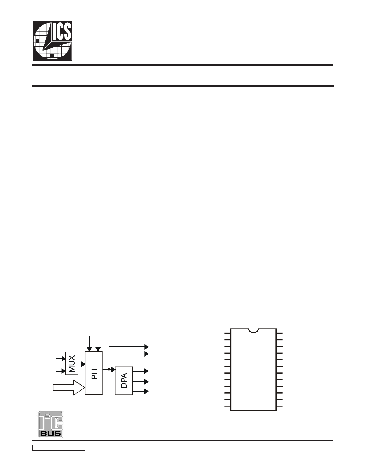
The ICS1524A is a low-cost, very high-performance
frequency generator and phase controlled clock synthesizer. It is perfectly suited to phase controlled clock
synthesis and distribution as well as line-locked and
genlocked applications.
The ICS1524A offers two channels of clock phase controlled outputs; CLK and DPACLK. These two output
channels have both 250 MHz PECL differential and 150
MHz SSTL_3 single-ended output pins. The CLK output
channel has a fixed phase relationship to the PLL’ s input
and the DPACLK uses the Dynamic Phase Adjust circuitry to allow control of the clock phase relative to input
signal.
Optionally , the CLK outputs can operate at half the clock
rate and phase aligned with the DPACLK channel, enabling deMUXing of multiplexed analog-to-digital
converters. The FUNC pin provides either the regenerated input from the phase-locked loop (PLL) divider
chain output or a re-synchronized and sharpened input
HSYNC.
The advanced PLL uses either its internal programmable feedback divider or an external divider and is
programmed by a standard I
2
C-bus™ serial interface.
• Wide input frequency range
• 8 kHz to 100 MHz
• 250 MHz balanced PECL differential outputs
• 150 MHz single-ended SSTL_3 clock outputs
• Dynamic Phase Adjust (DPA) for DPACLK
outputs
• Software controlled phase adjustment
• 360
o
Adjustment down to 1/64 clock
increments
• External or internal loop filter selection
• Uses 3.3 VDC Inputs are 5 volt tolerant.
2
C-bus serial interface runs at either low speed
•I
(100 kHz) or high speed (400 kHz).
• Hardware and Software PLL Lock detection
Applications
• Generic Frequency Synthesis
• LCD Monitors and Projectors
• Genlocking Multiple Video Systems
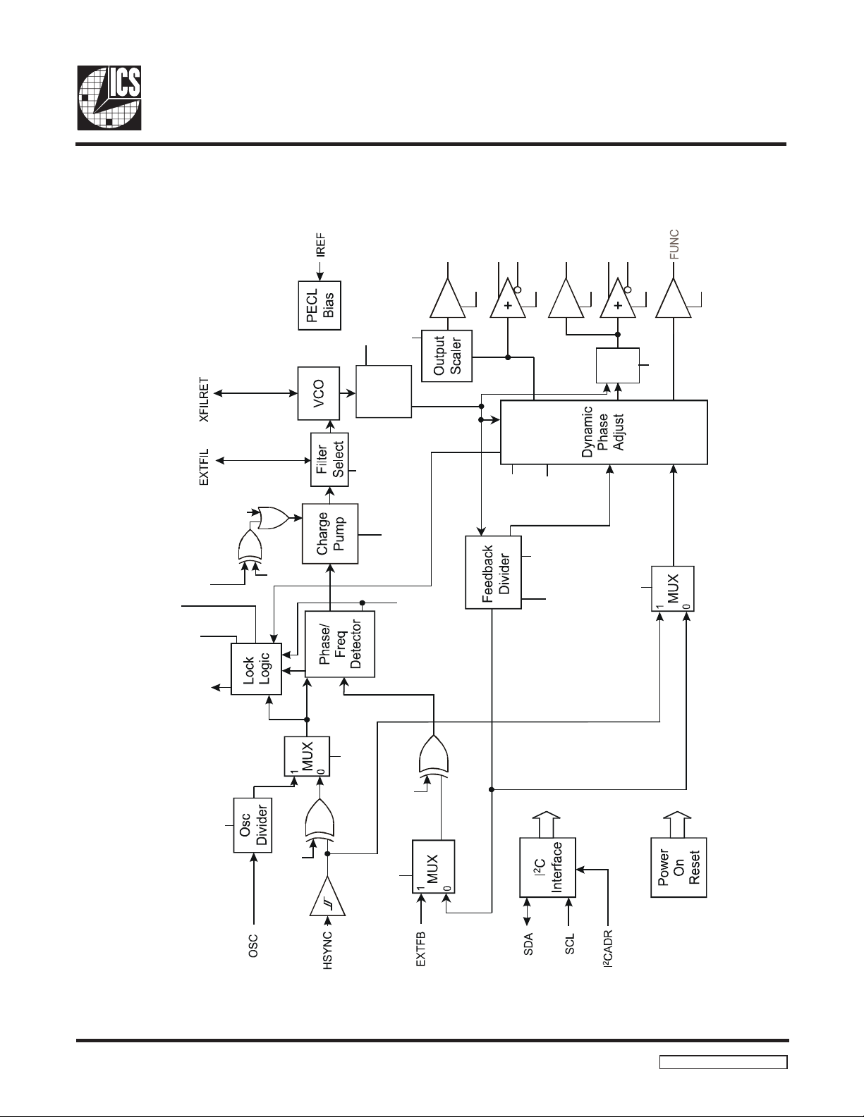
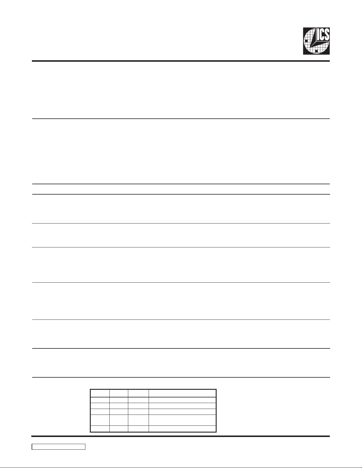
Block Diagram
HSYNC
OSC
2
IC
I2C-bus is a trademark of Philips Corporation.
ICS1524A Rev D 12/23/2005
Loop
Filter
CLK
CLK+/-
DPACLK
DPACLK+/-
FUNC
Pin Configuration
VDDD
VSSD
SDA
SCL
PDEN
EXTFB
HSYNC
EXTFIL
XFILRET
VDDA
VSSA
OSC
ICS reserves the right to make changes in the device data identified in this
publication without further notice. ICS advises its customers to obtain the
latest version of all device data to verify that any information being relied
upon by the customer is current and accurate.
1
2
3
4
5
6
7
8
9
10
11
12
24 Pin 300-mil SOIC
24
23
22
21
20
19
18
ICS1524A
17
16
15
14
13
IREF
CLK+ (PECL)
C
LK– (PECL)
DPACLK+ (PECL)
DPACLK– (PECL)
VSSQ
VDDQ
CLK (SSTL)
DPA
CLK (SSTL)
FUNC (SSTL)
LOCK/REF (SSTL)
2
ICADR

ICS 1524A
Document Revision History
Rev A
ICS1523 Rev T Datasheet used as a starting template
New Block Diagram substituted for old 1523 one
Removed reference to CLK / 2 Functionality
Created a set of clock outputs that bypass the DPA
External PDEN is now the IN-SEL MUX control bit
Text descriptions changed to support new 1524 block diagram
Rev B
Replaced page 15 “Layout Guidelines”
Replaced SIOC Package diagram on page 22
“Advanced Status” removed
Redrew front page graphics for clairity
Rev C
Corrected Chip Revision and Chip Version values on page 5
Changed Title on Page 1
Minor format changes to pages 8 and 21
Corrected pin names on page 10
Rev D Miscellaneous updates to Block Diagram on page 3
Changed reference from “Phase Detector” to “Charge Pump”. Pages 4-7, 10
ICS1524A Rev D 12/23/2005
2
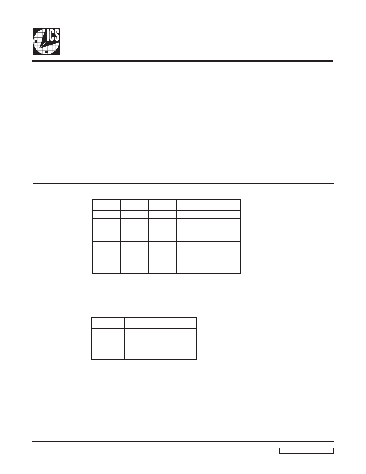
Block Diagram
DPACLK
DPACLK-
DPACLK+
CLK
CLK+
ICS1524A
CLK-
EnPLS
Reg 0:6
EnDLS
Reg 0:7
PDEN
PDEN
Reg 0x0:0
PD_Pol
Reg 0x0:1
PSD
Reg 0x1:4-5
POST
SCALER
Fill_Sel
Reg 0x4:7
PFD
Out_Scl
Reg 0x6:6-7
Divider
Reg 0x1:0-2
REG 12:1
PLL_LOCK
REG 12:0
DPA_LOCK
OE_Tck
Reg 0x6:1
OE_Pck
DPA_OS
Reg 0x4:0-5
Reg 0x6:0
DPA_Res
Reg 0x5:0-1
FBD
Reg 0x3:0-3
FBD
OE_T2
Reg 0x6:3
Reg 0x2:0-7
OE_P2
MUX
Func_Sel
Reg 0x0:5
Reg 0x6:2
Ck2_Inv
Reg 6:5
OE_F
Reg 0x6:4
LOCK/REF
Osc_Div
Reg 0x7:0-6
Ref_Pol
Reg 0x0:2
In_Sel
Reg 0x7:7
Fbk_Pol
Fbk_Sel
Reg 0x0:4
Reg 0x0:3
ICS1524A Rev D 12/23/2005
3
ICS 1524A
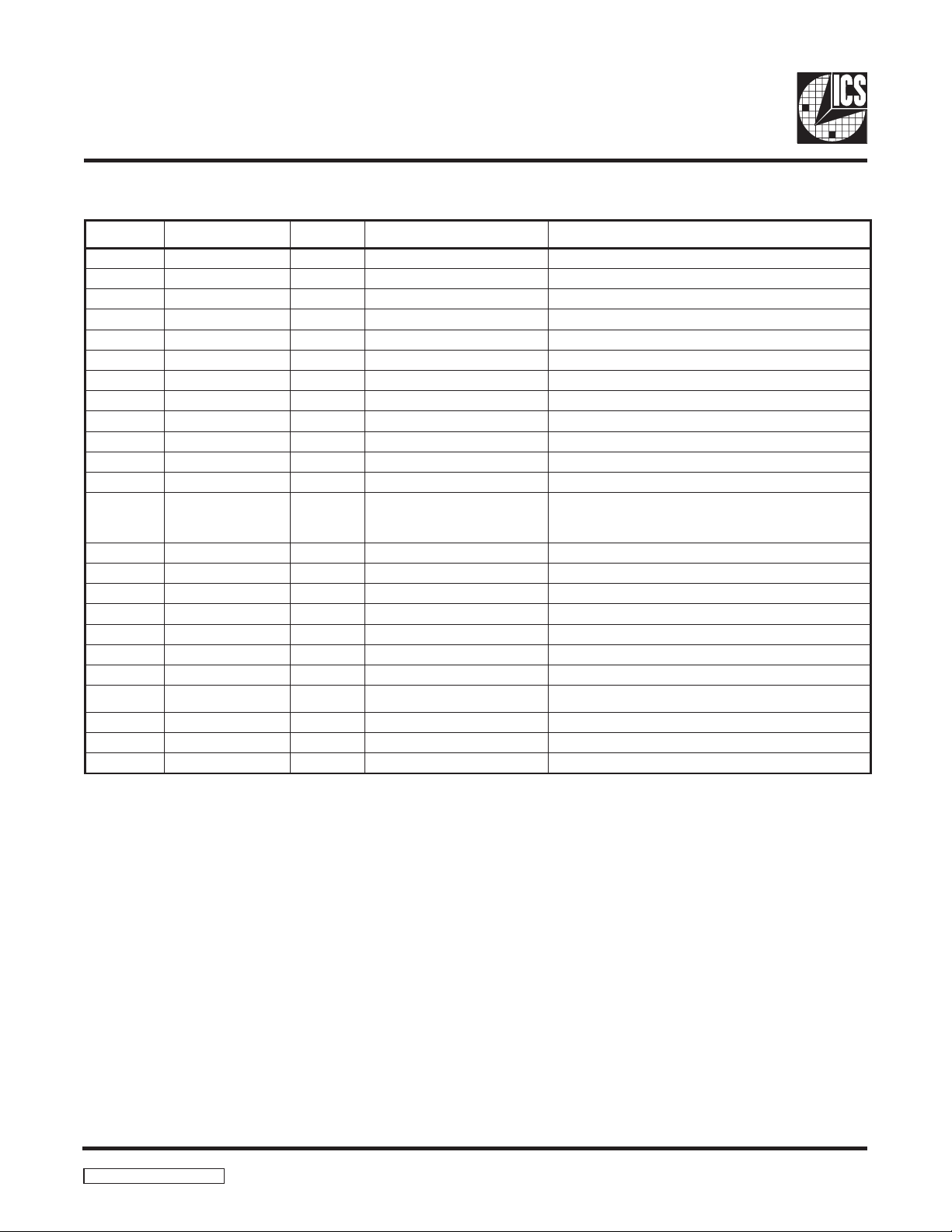
Pin Descriptions
.ONNIPEMANNIPEPYTNOITPIRCSEDSTNEMMOC
1DDDVRWPylppuslatigiDsnoitceslatigidotV3.3
2DSSVRWPdnuorglatigiDsnoitceslatigi
3ADSTUO/NIatadlaireSI
4LCSNIkcolclaireSI
2
2
5NEDPNIpmuPegrahCpmupegrahcsdnepsuS
6BFTXENIkcabdeeflanretxEottupniredividlanretxEDFP
7CNYSHNIcnyslatnoziroHLLPottupnikcolC
8LIFTXENIretliflanretxEretlifpoolLLPlanretxE
9TERLIFXNInruterretliflanretxEnruterretlifpoolLLPlanretxE
01ADDVRWPyl
ppusgolanAyrtiucricgolanarofV3.3
11ASSVRWPdnuorggolanAyrtiucricgolanarofdnuorG
21CSONIrotallicsOrotallicsolatsyr
31I2RDACNII2sserddaC
41FER/KCOLLTSSecnerefer/rotacidnikcoLtupniFERrokco
51CNUFLTSStuptuonoitcnuFtuptuoCNYSHelbatceles3_LTSS
61KLCLTSStkcolclexiPkcolC3_LTSSdeyaleD-no
N
71KLCAPDLTSSkcolCdeyaleDAPDkcolC3_LTSSdeyaleDAPD
81QDDVRWPylppusrevirdtuptuOsrevirdtuptuorofDDVV3.3
91QSSVRWPdnuo
02–KLCAPDLCEP-kcolcLCEPdeyaleDAPD .niardnepOkcolCLCEPdetrevnIdeyaleDAP
rgrevirdtuptuOsrevirdtuptuorofdnuorG
D
12+KLCAPDLCEP+kcolcLCEPdeyaleDAPD .niardnepOkcolCLCEPdeyaleDAPD
22–KLCLCEP-kcolcLCEP .niardnepOkcolCLCEPdetre
32+KLCLCEP+kcolcLCEP .niardnepOkcolCLCEPdeyaleD-noN
42FERINItnerrucecnerefeRstuptuoLCEProftnerru
drofdnuorG
1
sub-C
1
sub-C
cmorftupnIegakcap
2
IpihC
cecnerefeR
1
1
1
2,1
tcelessserddaC
etirwhC4,daerhD4=woL
etirwhE4,daerhF4=hgiH
lAPDroLLPsyalpsiD
vnIdeyaleD-noN
Notes:
1. These L VTTL input s are 5 V -tolerant.
2. Connect to ground if unused.
ICS1524A Rev D 12/23/2005
4
ICS1524A
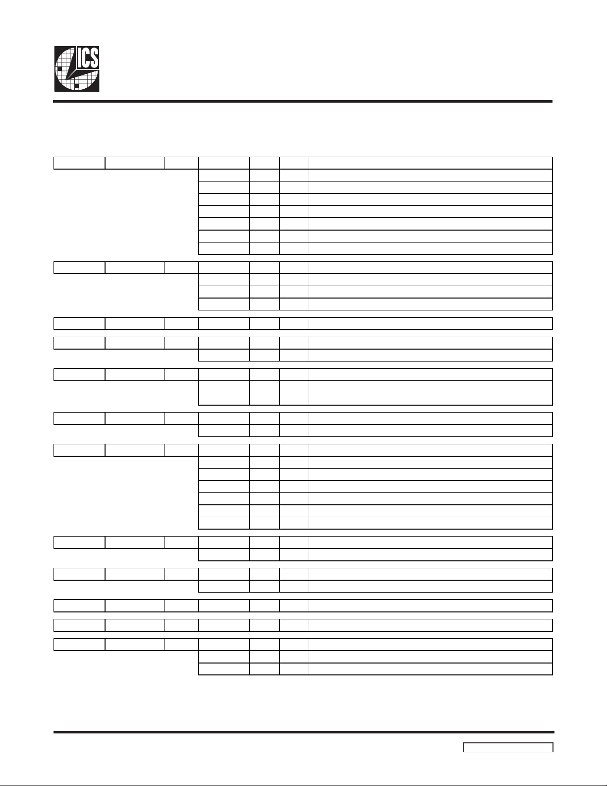
I2C Register Map Summary
Register
Index
0h Input Control R / W PDen 0 1 Charge Pump Enable (0=Disable 1=Enable)
1h Loop Control R / W * PFD0-2 0-2 0 Charge Pump Gain
2h FdBk Div 0 R / W * FBD0-7 0-7 FF PLL FeedBack Divider LSBs (bits 0-7) *
3h FdBk Div 1 R / W * FBD8-11 0-3 F PLL Feedback Divider MSBs (bits 8-11) *
Name Access Bit Name Bit #
PD_Pol 1 0 Cha rge Pum p Enable Polarity
Ref_Pol 2 0 External Reference Polarity (0=Positive Edge, 1=Negative Edge)
Fbk_Pol 3 0 External Feedb ack Polarit y (0=Positive Edge, 1=Negative Edge)
Fbk_Sel 4 0 External Feedback Selec t (0=Internal Feedback, 1=External)
Func_Sel 5 0 Function Out Select (0=Recovered HSYNC, 1=Input HSYNC)
EnPLS 6 1 Enable PLL Lock/Ref Status Output (0=Disable 1=Enable)
EnDLS 7 0 Enable DPA Lock/Ref Status Output (0=Disable 1=Enable)
Reserved 3 0 Reserved
PSD0-1 4-5 0 Post-Scaler Divider (0 = /2, 1 = /4, 2 = /8, 3 = /16)
Reserved 6-7 0 Reserved
Reserved 4-7 0 Reserved
Reset
Value
Description
4h DPA Offset R / W DPA_OS0-5 0-5 0 Dynamic Phase Aligner Offset
Reserved 6 0 Reserved
Fil_Sel 7 1 Loop Filter Select (0=External, 1=Internal)
5h DPA Control R / W ** DPA_Res0-1 0-1 3 DPA Resolution (0=16 delay elements, 1=32, 2=Reserved, 3=64)
Metal_Rev 2-7 0 Metal Mask Revision Number
6h Output Enables R / W OE_Pck 0 1 Output Enable for PECL DPACLK ( 0=High Z, 1=Enabled)
OE_Tck 1 1 Output Enable for STTL_3 DPACLK ( 0=High Z, 1=Enabled)
OE_P2 2 1 Output Enable for PECL CLK ( 0=High Z, 1=Enabled)
OE_T2 3 1 Output Enable for STTL_3 CLK ( 0=High Z, 1=Enabled)
OE_F 4 1 Output Enable for STTL_3 FUNC ( 0=High Z, 1=Enabled)
Ck2_Inv 5 0 Select non-delayed CLK (1) or DPA delayed CLK/ 2 (0) on CLK x pins
Out_Scl 6-7 0 SSTL DPACLK (Pin 17) Sc aler (0 = ÷1, 1 = ÷2, 2 = ÷4, 3 = ÷8)
7h Osc_Div R / W Osc_Div 0-6 0-6 0 Osc Divider modulus
In-Sel 7 1 RESERVED
8h Reset Write DPA 0-3 x Writing xA hex resets DPA and loads working register 5
PLL 4-7 x Writing 5x hex resets PLL and loads working registers 1-3
10h Chip Ver Rea d Chip Ver 0- 7 18 Chip Version 17 hex
11h Chip Rev Read Chip Rev 0-7 01 Chip Revision C2 hex
12h Rd_Reg Read DPA_Lock 0 N/A DPA Lock Status (0=Unlocked, 1=Locked)
PLL_Lock 1 N/A PLL Lock Status (0=Unlocked, 1=Locked)
Reserved 2-7 0 Reserved
* Identifies double-buffered registers. Working registers are loaded during software PLL reset.
** Identifies double-buffered register. Working registers are loaded during software DPA reset.
5
ICS1524A Rev D 12/23/2005
ICS 1524A
Detailed Register Description
Name: Input Control
Register: 0 h
Index: Read / Write
Bit Name Bit # Reset Value Description
PDen 0 1 Charge Pump Enable
PD_Pol 1 0 Charge Pump Enable Polarity
Ref_Pol 2 0 External Reference Polarity
Fbk_Pol 3 0 External Reference Feedback Polarity
Fbk_Sel 4 0 External Feedback Select
Func_Sel 5 0 Function Output Select
EnPLS 6 1 Enable PLL Lock Status Output on LOCK/REF pin
EnDLS 7 0 Enable DPA Lock Status Output on LOCK/REF pin
Bit Name Description
0 PDen Charge Pump Enable
0 = External Enable via PDEN pin
1 = Always Enable
1 PD_Pol Charge Pump Enable Polarity
0 = Active High
1 = Active Low
2 Ref_Pol External Reference Polarity —
Edge of input signal on which Phase/Frequency Detector triggers.
0 = Rising Edge (default)
1 = Falling Edge
3 Fbk_Pol External Reference Feedback Polarity — Edge of EXTFB (pin 6) signal on which
Phase/Frequency Detector triggers when external feedback is used (Reg0 [4]=1).
0 = Positive Edge (default)
1 = Negative Edge
4 Fbk_Sel External Feedback Select
0 = Internal Feedback (default)
1 = External Feedback
5 Func_Sel Function Output Select — Selects re-clocked output to FUNC (pin 15).
0 = Recovered HSYNC (default). Regenerated HSYNC output.
1 = External HSYNC. Schmitt-trigger conditioned input from HSYNC (pin 7).
6 EnPL S Enable LOCK/REF (pin14) Output
7 EnDLS
ICS1524A Rev D 12/23/2005
SLPnESLDnELES_NI)41(FER/KCOL
00 A/N0
01 A/Nesiwrehto0,dekcolAPDfi1
10 A/Nesiwrehto0,dekcolLLPfi1
110
111 F
÷ viD_csO
cso
6
reggirtttimhcStsoP
feRROX)7(CNYSH
loP_
Name: Loop Control Register
Register: 1h
Index: Read / Write*
Bit Name Bit # Reset Value Description
PFD0-2 0-2 0 Charge Pump Gain
Reserved 3 0 Reserved
PSD0-1 4-5 0 Post-Scaler Divider
Reserved 6-7 0 Reserved
Bit Name Description
0-2 PFD0-2 Charge Pump Gain
2tiB1tiB0tiB2/Aµ(niaGCP π )dar
000 1
001 2
010 4
011 8
100 61
10 1 23
110 46
111 82
ICS1524A
1
3 Reserved
4-5 PSD0-1 Post-Scaler Divider — Divides the output of the VCO to the DPA and Feedback Divider.
5tiB4tiBrediviDDSP
00 )tluafed(2
01 4
10 8
11 61
6-7 Reserved
Double-buffered register . Actual working registers are loaded during software PLL reset.
*
See register 8h for details.
7
ICS1524A Rev D 12/23/2005
ICS 1524A
Name: Feedback Divider 0 Register / Feedback Divider 1 Register
Register: 2h, 3h
Index: Read /Write*
Bit Name Index Bit # Reset Value Description
FBD0-7 2 0-7 FF PLL Feedback Divider LSBs (0-7).* When Bit 0 = 0, then the total
number of clocks per line is even. When Bit 0 = 1, then the total
number of clocks is odd.
FBD8-11 3 0 -3 F PLL Feedback Divider MSBs (8-11)*
Reserved 3 4-7 Reserved
The value that is programmed into these two registers, plus a value of 8, defines the total number of clock periods that the ICS
1524 generates between HSYNCs. Program these registers with the total number of horizontal clocks per line minus 8.
3geR2geR
321076543210
Feedback Divider Modulus
=
12 ≤ Feedback Divider Modulus ≤ 4103
+8
Double-buffered registers. Actual working registers are loaded during software PLL reset.
*
See Register 8h for details.
Name: DPA Offset Register
Register: 4 h
Index: Read /Write
Bit Name Bit # Reset Value Description
DPA_OS0-5 0-5 0 Dynamic Phase Adjust Of fset
Reserved 6 0 Reserved
Fil_Sel 7 0 Loop Filter Select
Bit Name Description
0-5 DPA_OS0-5 Dynamic Phase Adjust Offset.
Selects clock edge offset in discrete steps from zero to one clock period minus one step.
Resolution (number of delay elements per clock cycle) is selected by DPA_Res0-1 (Reg 5:0-1).
Note: Offsets equal to or greater than one clock period are neither recommended nor supported.
Example: For DPA_Res0-1=01H, the clock can be delayed from 0 to 31 steps.
7 Fil_Sel Selects external loop filter (0) or internal loop filter (1).
The use of an external loop filter is strongly recommended for all designs. Typical loop filter
values are 6.8K Ohms for the series resistor, 3300 pF RF-type capacitor for the series capacitor,
and 33 pF for the shunt capacitor.
ICS1524A Rev D 12/23/2005
8

Name: DPA Control Register
Register: 5h
Index: Read / Write*
Bit Name Bit # Reset Value Description
DPA_Res0-1 0-1 3 Dynamic Phase Adjust Resolution Select.
Metal_Rev 2-7 0 Metal Mask Revision Number.
Bit Name Description
0-1 DPA_Res0-1 Dynamic Phase Adjust (DPA) Resolution Select.
It is not recommended to use the DPA above 160 MHz.
ICS1524A
Bit 1 Bi t 0 Delay Elements
0 0 16 48 160
0 1 32 24 80
10 Reserved
1 1 64 12 40
2-7 Metal_Rev Metal Mask Revision Number.
After power-up, register bits 7:2 must be written with 1 11111. After this write,
a read indicates the metal mask revision, as below .
noisiveR7tiB6tiB5tiB4tiB3tiB2tiB
A 111111
B 011111
1C 101111
2C 001111
D110111
E 111011
F 111101
G 111110
CLK Range, MHz
Double-buffered register . Actual working registers are loaded during software DPA reset.
*
See register 8h for details.
9
ICS1524A Rev D 12/23/2005

ICS 1524A
Name: Output Enable Register
Register: 6 h
Index: Read / Write
Bit Name Bit # Reset Value Description
OE_Pck 0 0 Output Enable for DPACLK Outputs (PECL, Pins 21, 20 )
OE_T ck 1 0 Output Enable for DPACLK Output (SSTL_3 Pin 17)
OE_P2 2 0 Output Enable for CLK Outputs (PECL, Pins 23, 22)
OE_T2 3 0 Output Enable for CLK Output (SSTL_3, Pin 16)
OE_F 4 0 Output Enable for FUNC Output (SSTL_3, Pin 15)
CK2_Inv 5 0 Select CLK Output Source (Pins 23, 22, 16)
Out_Scl 6-7 0 DPACLK Output Scaler (SSTL_3, Pin 17)
Bit Name Description
0 OE_Pck Output Enable for DPACLK Outputs (PECL)
0 = High Z
1 = Enabled
1 OE_Tck Output Enable for DPACLK Output (SSTL_3)
0 = High Z
1 = Enabled
2 OE_P2 Output Enable for CLK Outputs (PECL)
0 = High Z
1 = Enabled
3 OE_T2 Output Enable for CLK Output (SSTL_3)
0 = High Z
1 = Enabled
4 OE_F Output Enable for FUNC Output (SSTL_3)
0 = High Z
1 = Enabled
5 Ck2_Inv Select CLK Output Source (Pins 23, 22, 16)
0 = Half Speed DPA Delayed clock to CLK outputs
1 = Full Speed non-DPA Delayed clock to CLK outputs
6-7 Out_Scl Clock (DPACLK, pin 17) Scaler
Bit 7
00 1
01 2
10 4
11
Bit 6
DPACLK Divider
8
ICS1524A Rev D 12/23/2005
10

Name: Oscillator Divider Register
Register: 7h
Index: Read / Write
Bit Name Bit # Reset Value Description
Osc_Div 0-6 0-6 0 Osc Divider Modulus
In_Sel 7 1 Input Select
Bit Name Description
0-6 Osc_Div 0-6 Oscillator Divider Modulus.
Divides the input from OSC (pin 12) by the set modulus.
The modulus equals the programmed value, plus 2.
Therefore, the modulus range is from 3 to 129.
7 In_Sel Input Select — Selects the input to the Phase/Frequency Detector
0 = HSYNC
1 = Osc Divider
ICS1524A
Name: RESET Register
Register: 8 h
Index: Write
Bit Name Bit # Reset Value Description
DPA Reset 0-3 x Writing xAh to this register resets DPA working register 5
PLL Reset 4-7 x Writing 5xh to this register resets PLL working registers 1-3
Bit Name Description
0 -3 DPA Writing xAh to this register resets DPA working register 5
4-7 PLL Writing 5xh to this register resets PLL working registers 1-3
eulaVsteseR
AxAPD
x5LLP
A5LLPdnaAPD
11
ICS1524A Rev D 12/23/2005

ICS 1524A
Name: Chip Version Register
Register: 10h
Index: Read
Bit Name Bit # Reset Value Description
Chip Ver 0-7 17 Chip Version 24 (18h)
Name: Chip Revision Register
Register: 11h
Index: Read
Bit Name Bit # Reset Value Description
Chip Rev 0 -7 01+ Initial value 01h.
+V alue increments with each all-layer change.
Name: Status Register
Register: 12h
Index: Read
Bit Name Bit # Reset Value Description
DPA_Lock 0 N/A DPA Lock S tatus
PLL_Lock 1 N/A PLL Lock Status
Reserved 2-7 0 Reserved
Bit Name Description
0 DPA_Lock DPA Lock Status. (Refer to Register 0h, bits 6 and 7.)
0 = Unlocked
1 = Locked
1 PLL_Lock PLL Lock Status. (Refer to Register 0h, bits 6 and 7.)
0 = Unlocked
1 = Locked
2-7 Reserved
ICS1524A Rev D 12/23/2005
12

I2C Data Characteristics
ICS1524A
Bit transfer on the I2C-bus
START and STOP conditions
Acknowledge on the I2C-bus
These waveforms are from "The I2C-bus and how to use it," published by Philips Semiconductor.
The document can be obtained from http://www-us2.semiconductors.philips.com/acrobat/various/i2c_bus_specification_1995.pdf
13
ICS1524A Rev D 12/23/2005

ICS 1524A
I2C Data Format
RANDOM REGISTER WRITE PROCEDURE
S010011xWA A AP
7 bit address register address dat
Acknowledge Acknowledge STOP condition
START condition WRITE command Acknowledge
RANDOM REGISTER READ PROCEDURE
S010011XWA AS010011XRA AP
7 bit address register address 7 bit address dat
Acknowledge Repeat START Acknowledge STOP condition
START condition WRITE command Acknowledge READ command NO Acknowledge
SEQUENTIAL REGISTER WRITE PROCEDURE
S010011XWA A A A AP
7 bit address register address dat
Acknowledge Acknowledge Acknowledge Acknowledge Acknowledge
START condition WRITE command STOP condition
a
a
a data
SEQUENTIAL REGISTER READ PROCEDURE
S010011XWA AS010011XRA A AP
7 bit address register address 7 bit address dat
Acknowledge Repeat START Acknowledge NO Acknowledge
START condition WRITE command Acknow ledge READ command Acknowledge STOP condition
Direction
: From bus host to device From device to bus host
a data
Note:
1. All values are transmitted with the most-significant bit first and the least-significant bit last.
2. The value of the X bit equals the logic state of pin 13 (I
2
CADR).
3. R = READ = 1 and W = WRITE = 0
ICS1524A Rev D 12/23/2005
14

General Layout Guidelines
• Use a PC board with at least four layers: one power, one ground, and two signal.
• Use at least one 4.7 uF T ant alum (or similar) capacitor for global VDD bulk decoupling.
• All supply voltages must be supplied from a common source and must ramp together.
• Any flux or other board surface debris can degrade the performance of the external loop filter.
• Ensure that the 1524A area of the board is free of contaminants.
ICS1524A
Specific Layout Guidelines
1. Digital Supply (VDD) – Bypass pin 1 (VDD) to pin 2 (VSS) a 0.1-µF capacitor, located as close as possible to the pins. A
0.01-µF capacitor may be added for additional high frequency rejection.
2. External Loop Filter – Strongly recommended in
(EXTFIL and EXTFILRET) as possible with minimum length traces. Typical loop filter values are 6.8K Ohms for the
series resistor, 3300 pF RF-type capacitor for the series capacitor, and 33 pF for the shunt capacitor. (For details, see
the Frequently Asked Questions part of the ICS1523 Applications Guide, FAQ2 and FAQ3.) A ground isolated, surface
trace can be useful to isolate this section from the rest of the board.
3. Analog PLL Supply (VDDA) – Decouple main VDD from pin 10 (VDDA) with a series ferrite bead. Bypass the supply end
of the bead with 4.7-µF. Bypass pin 10 to pin 11 (VSSA) with a 0.1-µF capacitor. A 0.01-µF capacitor may be added for
additional high frequency rejection. Locate these components as close as possible to the pins.
4. PECL Current Set Resistor – Locate PECL current-set resistor as close as possible to pin 24 (IREF). Bypass pin 24 to
ground with a 0.1 -µF capacitor.
.
5. PECL Outputs – Implement these outputs as microstrip transmission lines. The trace widths shown are for 75 Ohm
characteristic impedance. Locate any optional series “snubbing” resistors as close as possible to the source pins. If
the termination resistors are included on-board, locate them as close as possible to the load and connect directly to the
power and ground planes.
[These termination resistors are omitted if the load device implements them internally. For details, see the ICS applica-
tion note on microstrip and striplines (1572AN1) and within the ICS1523 Applications Guide, the application note on
Designing a Custom Interface for the ICS1523 (1523AN4.)]
All Designs. Locate loop filter components as close to pins 8 and 9
6. Output Driver Supply – Bypass pin 18 (VDDQ) to pin 19 (VSSQ) with a 0.1-µF capacitor, located as close as possible
to the pins. A 0.01-µF capacitor may be added for additional high frequency rejection.
7. SSTL_3 Outputs – SSTL_3 outputs can be used like conventional CMOS rail-to-rail logic or as a terminated transmission line system at higher-output frequencies. With terminated outputs, the considerations of item 5, “PECL Outputs”
apply. See JEDEC documents JESD8-A and JESD8-8.
ICS1524A Rev D 12/23/2005
15

ICS 1524A
PECL Outputs
For information on using the ICS1524A’s PECL output pins, please refer to Application Note 4: Designing a Custom
PECL Interface for the ICS1523
SSTL_3 Outputs
Unterminated Outputs
In the ICS1524A, unterminated SSTL_3 output pins display exponential transitions similar to those of rectangular
pulses presented to RC loads. The 10-90% rise time is typically 1.6 ns, and the corresponding fall time is typically
700 ps. In turn, this asymmetry contributes to duty cycle asymmetry at higher output frequencies. In the absence of
significant load capacitance (which can further increase rise and fall time), this asymmetry is the dominant factor
determining high-frequency performance of these single-ended outputs. T ypically , no termination is required either for
the LOCK/REF , FUNC, and CLK/2 output s or for CLK outputs up to approximately 135 MHz.
T erminated Output s
SSTL_3 outputs are intended to terminate in low impedances to reduce the effect of external circuit capacitance.
Use of transmission line techniques enables use of longer traces between source and driver without increasing
ringing due to reflections. Where external capacitance is minimal and substantial voltage swing is required to meet
L VTTL V
by termination in a low impedance.
and VOL requirements, the intrinsic rise and fall times of ICS1524A SSTL outputs are only slightly improved
IH
The ICS1524A SSTL output source impedance is typically less than 60 Ohms. Termination impedance of 100 Ohms
reduces output swing by less than 30% which is more than enough to drive a single load of L VTTL inputs.
D
VD
Ω
ICS1524A
For more information on using the ICS1524A’s SSTL output pins, please refer to Application Note 3: Using SSTL_3
Outputs with CMOS or L VTTL Input s
SSTL-3 Output
330
150
Ω
Single
LV TTL
Load
ICS1524A Rev D 12/23/2005
16

ICS1524A
Power Supply Considerations
The ICS1524A incorporates special internal power-on reset circuitry that requires no external reset signal connection. The supply voltage (VDD) must remain within the recommended operating conditions during normal operation. T o reset the ICS1524A,
the supply voltage at the part must be reduced below the threshold voltage (V
age must remain below that threshold voltage such that board power conditioning capacitors are drained and the proper reset
state is latched. The amount of time (t
10 ms should be sufficient.
Supply
Vo lt ag e
) to hold the voltage in a reset state varies with the design. However, a typical value of
d
t
d
) of the power-on reset circuit. The supply volt-
th
V
min
V = 1.8V
th
Absolute Maximum Ratings
VDD, VDDA, VDDQ (measured to VSS) . . . . . . . . . . . . . . . . . 4.3 V
Digital Inputs . . . . . . . . . . . . . . . . . . . . . . . . . . . . . . . . . . . . . . . . VSS –0.3 V to 5.5 V
Analog Outputs. . . . . . . . . . . . . . . . . . . . . . . . . . . . . . . . . . . . . . . VSSA –0.3 V to VDDA +0.3 V
Digital Outputs . . . . . . . . . . . . . . . . . . . . . . . . . . . . . . . . . . . . . . . VSSQ –0.3 V to VDDQ +0.3 V
Storage Temperature . . . . . . . . . . . . . . . . . . . . . . . . . . . . . . . . . . . –65°C to +150°C
Junction Temperature . . . . . . . . . . . . . . . . . . . . . . . . . . . . . . . . . . 175°C
Soldering Temperature . . . . . . . . . . . . . . . . . . . . . . . . . . . . . . . . . 260°C
ESD Susceptibility* . . . . . . . . . . . . . . . . . . . . . . . . . . . . . . . . . . > 2 KV
(*Electrostatic-sensitive devices. Do not open or handle except in a static-free workstation.)
17
ICS1524A Rev D 12/23/2005

ICS 1524A
Recommended Operating Conditions
VDD, VDDQ, VDDA (measured to VSS). 3.0 to 3.6 V
Operating Temperature (Ambient). . . . . . 0 to +70°C
tnerruCylppuSCD
RETEMARAPLOBMYSSNOITIDNOCNIMXAMSTINU
latigiD,tnerruCylppuSDDDIV6.3=DDDV—52Am
srevirDtuptuO,tnerruCylppuSQDDI.delban
golanA,tnerruCylppuSADDIV6.3=ADDV—5Am
RETEMARAPLOBMYSSNOITIDNOCNIMXAMSTINU
egatloVhgiHtupnIHIV25.5V
egatloVwoLtupnILIV3.0-SSV8.0V
siseretsyHtupnI 2.06.0V
uChgiHtupnIHIIVHIDDV=—01±Aµ
tnerr
tnerruCwoLtupnILIIV
ecnaticapaCtupnIniC—01Fp
0=—002±Aµ
LI
esrevirdtuptuoon,V6.3=QDDV—6Am
2
,CSO,CNYSH,BFTXE,NEDP,LCS,ADS(stupnIlatigiDI
C)RDA
)lanoitceridiBsiADS:edoMtuptuOnI(ADS
RETEMARAPLOBMYSSNOITIDNOCNIMXAMSTINU
egatloVwoLtuptuOLOV
RETEMARAPLOBMYSSNOITIDNOCNIMXAMSTINU
egatloVhgiHtuptuOHOV0=TUOI—DDVV
ycneuqerFtuptuOmumixaMXAMpFV3.3=DDDV—052zHM
loVwoLtuptuO
egat
ebnacTUOIrofeulav
).deniatniam
(stuptuO3-LTSS
ecnatsiseRtuptuOR
wolebllaftontsumLOV:etoN(
tcerrocehttahtosnevigleveleht
APD
RETEMARAPLOBMYSSNOITIDNOCNIMXAMSTINU
ycneuqerFtuptuOmumixaMXAMsFV3.3=DDDV—051zHM
LOVeula
O
V<1
O
scitsiretcarahCtupnICA
RETEMARAPLOBMYSSNOITIDNOCNIMXAMSTINU
ycneuqerFtupnICNYSHf
ycneuqerFtupnICSOf
CNYSH
CSO
samumixamV0.6=HOV.Am3=TUOI
tybdenimreted
KLC,+KLC,–KLCAPD,+KLCAPD(stuptuOLCEP
)-
vdemmargorp=TUOI0.1—V
KCOL,CNUF,KLC,KLC
V2<—08
)FER/
.rotsiserpu-lluplanretxeeh
800.01zHM
20.001zHM
4.0V
Ω
ICS1524A Rev D 12/23/2005
18

700
ICS1524A
VCO O utput Fr equency and Intrinsic Jit ter
700
600
500
400
300
VCO Frequency (MHz)
200
100
0
0
2
.
0
0
Frequency (Slow: 3.0V @ 70 ºC)
Frequency (Nominal: 3.3V @ 30ºC)
Frequency (Fast: 3.6V @ 0ºC)
Jitter (3.0V @ 70ºC)
Jitter (3.3V @ 30ºC)
Jitter (3.6V @ 0ºC)
Frequency
1
8
6
4
.
0
.
.
0
Jitter
2
2
.
.
1
1
1
VCO Voltage
.
.
1
8
6
4
2
.
2
2
6
4
.
.
2
2
3
8
.
2
.
3
600
500
400
300
200
100
Jitter (ps)
0
Note: Measured with an Externally Forced Filter Voltage
19
ICS1524A Rev D 12/23/2005

ICS 1524A
20
18
16
14
12
10
ns Delay
8
6
4
2
0
45
40
35
30
25
20
ns Delay
15
10
5
0
DPA Delay-16 Elemen t Reso l ution
50 MHz - SVGA @ 72 Hz
157.5 MHz - SXGA @ 85 Hz
04812
16
DPA Settin g
DPA Delay - 32 Element Resol u tion
25.175 MHz - VGA @ 60 Hz
78.75 MHz - XGA @ 75 H z
0 4 8 1216202428
DPA Setting
32
90
80
70
60
50
40
ns Delay
30
20
10
0
ICS1524A Rev D 12/23/2005
DPA Delay - 64 Elemen t Reso lu tio n
12.27 MHz - NTSC
39.8 MHz - SVGA @ 60
0 4 8 12 16 20 24 28 32 36 40 44 48 52 56 60
Note:
Maximum number of data points used for this graph.
DPA Setting
20
64

HSYNC
ICS1524A
t
0
REF
PECL CLKPECL CLK+
SSTL-CLK
FUNC_OUT
PECL DPACLKPECL DPACLK+
Output Timing Diagram
SSTL-DPACLK
FUNC
t
R
t
1
t
S
t
F
t
5
t
S
Typical Transition Times*
t
2
t
4
t
DPA
t
1
t
F
t
3
t
8
t
2
t
4
t
t
3
t
8
t
p
9
t
p
t
9
lobmySnoitpircseDgnimiTesiRllaFstinU
t
R
t
P
t
S
t
F
FER8.28.1sn
KLCLCEP0.12.1sn
KLC-LTSS6.17.0sn
TUO_CNUF2.10.1sn
Output Timing*
lobmySnoitpircseDgnimiTniMpyTxaMstinU
t
0
t
1
t
2t,3
t
4
t
5
t
6
t
7
t
8t,9
*Note: Measured at 3.6V 0°C, 135-MHz output frequency, PECL clock lines to 75 Οηµ termination, SSTL_3 clock lines
unterminated, 20-pF load. Transition times vary based on termination.
yaledFERotCNYSH3.115.1121sn
yaledkcolcLCEPotFER0.1-8.02.2sn
elcycytudkcolcLCEP540555%
yaledkcolc3_LTSSotkcolcLCEP2.057.02.1sn
yaledTUO_CNUFotkcolcLCEP5.19.13.2sn
kcolc2/LCEPotkcolcLCEP0.13.15.1sn
yaled2/KLC–3_LTSSotkcolcLCEP1.14.18.1sn
elcycytudkcolcLTSS540555%
21
ICS1524A Rev D 12/23/2005

ICS 1524A
ICS1524AM
ICS1524AMT
1524AM
1524AM
ICS1524AMLF
ICS1524AMLF
ICS1524AMLFT
1524AMLF
1524AMLF
SOIC-24
SOIC-24
Tape and Reel
Tubes
24-Pin SOIC (wide body)
noitamrofnIgniredrO
redrO/traP
rebmuN
M4251SCIM4251SCI42-COISsebuT
TM4251SCIM4251SCI42-COI
While the information presented herein has been checked for both accuracy and reliability, Integrated Circuit Systems, Incorporated (ICS) assumes no responsibility for either its use or
for infringement of any patents or other rights of third parties, which would result from its use. No other circuits, patents, or licenses are implied. This product is intended for use in normal
commercial applications. Any other applications such as those requiring extended temperature range, high reliability, or other extraordinary environmental requirements are not recommended without additional processing by ICS. ICS reserves the right to change any circuitry or specifications without notice. ICS does not authorize or warrant any ICS product for use in
life support devices or critical medical instruments.
ICS1524A Rev D 12/23/2005
gnikraMegakcaPgnippihS
SleeRdnaepaT
22

NOTES
ICS1524A
23
ICS1524A Rev D 12/23/2005

ICS 1524A
Corporate Headquarters: 2435 Boulevard of the Generals
San Jose Operations: 525 Race Street
Integrated Circuit Systems, Inc.
P.O. Box 968
Valley Forge, PA 19482-0968
Telephone: 610-630-5300
Fax: 610-630-5399
San Jose, CA 95126-3448
Telephone: 408-297-1201
Fax: 408-925-9460
Web Site: http://www.icst.com
ICS1524A Rev D 12/23/2005
24

 Loading...