

Page 1

k
查询ICS97ULP844A供应商
Integrated
ICS97ULP844A
Circuit
Systems, Inc.
1.8V Low-Power Wide-Range Frequency Clock Driver
Recommended Application:
• DDR2 Memory Modules / Zero Delay Board Fan Out
• Provides complete DDR DIMM logic solution with
ICSSSTU32864/SSTUF32864/SSTUF32866
Product Description/Features:
• Low skew, low jitter PLL clock driver
• 1 to 4 differential clock distribution (SSTL_18)
• Feedback pins for input to output synchronization
• Spread Spectrum tolerant inputs
• Auto PD when input signal is at a certain logic state
Switching Characteristics:
• Period jitter: 40ps
• Half-period jitter: 60ps
• CYCLE - CYCLE jitter 40ps
• OUTPUT - OUTPUT skew: 40ps
Pin Configuration
12 34 5
A
B
C
D
E
F
28-Ball BGA
Top View
Block Diagram
OE
OS
AV
DD
CLK_IN T
CLK_I NC
10K-100
GND
FB_INT
FB_I NC
* The Logic Detect (LD) powers down the device when a
logic low is applied to both CLK_INT and CLK_INC.
1110B—06/06/05
Powerdown
Control and
Test Logic
LD*
PLL
LD* or OE
PLL bypass
CLKT0
CLKC0
CLKT1
CLKC1
CLKT2
CLKC2
CLKT3
CLKC3
FB_OUTT
FB_OUTC
Ball Assignments
12345
A CLKT0 CLKC0 CLKC1 CLKT1 FB_INT
B CK_ INT V
C CK_ INC OE V
D A G ND GND V
E AV DD GND NB GND GND
F CLKC3 CLKT3 CLKC2 CLKT2 GND
DD
NB V
DD
DD
GND FB_OUTT
FB_INC
DD
OS FB_OUTC
Page 2
ICS97ULP844A
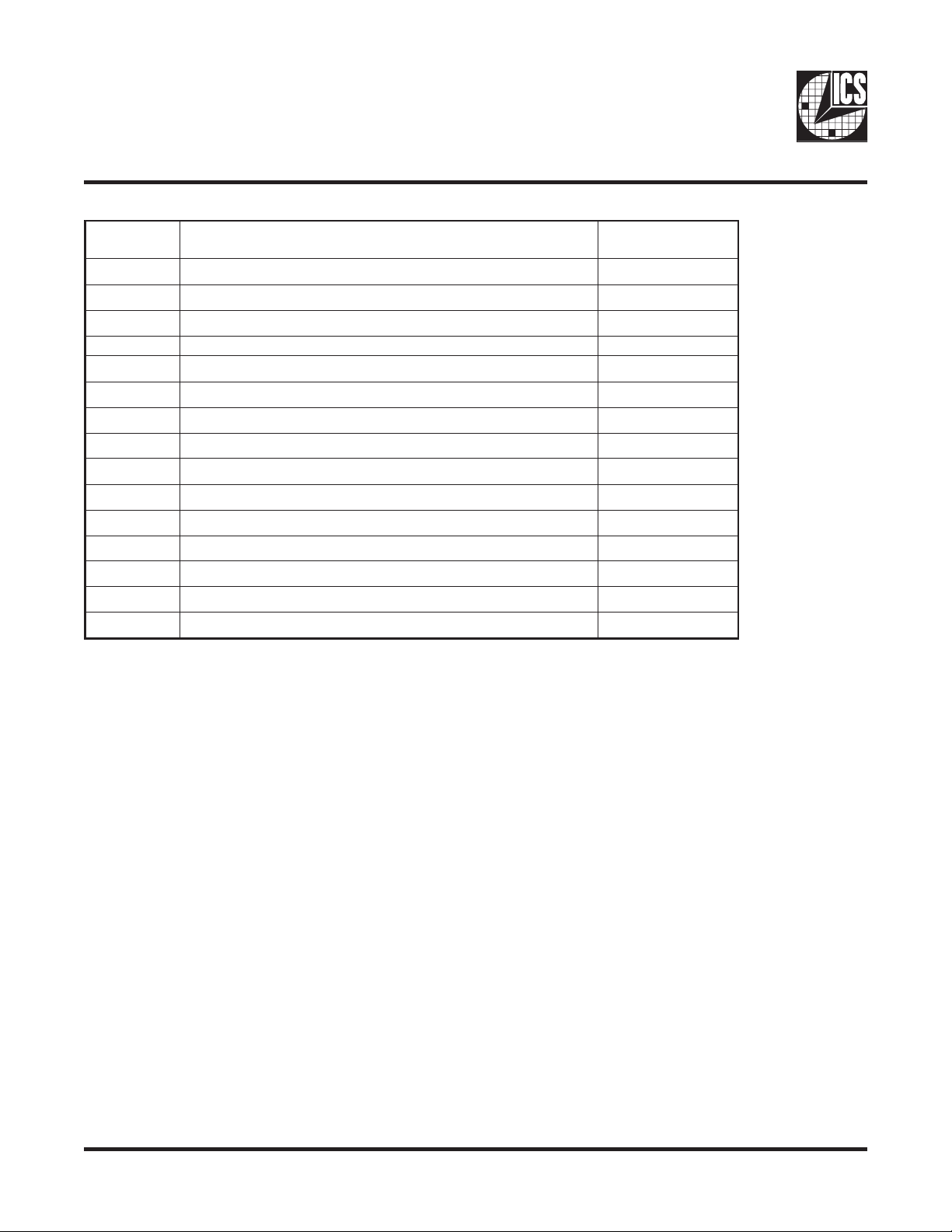
Pin Descriptions
lanimreT
emaN
DNGAdnuorGgolanA dnuorG
VA
DD
TNI_KLCrotsisernwodllup)mhOK001-K01(ahtiwtupnikcolC tupnilaitnereffiD
CNI_KLC rotsi
TNI_BFtupnikcolckcabdeeF tupnilaitne
CNI_BFtupnikcolckcabdeefyratnemelpmoC tupnilaitnereffiD
TTUO_BFtuptuokcolckcabdeeF tuptuolaitnereffi
CTUO_BFtuptuokcolckcabdeefyratnemelpmoC tuptuolaitnereffiD
EO)suonorhcnysA(elbanEtuptuO tupniSOMCVL
SOVroDN
DNGdnuorG dnuorG
V
QDD
]3:0[TKLCstuptuokcolC stuptuolaitnereffiD
C stuptuolaitnereffiD
]3:0[CKLCstuptuokcolcyratnemelpmo
BNllaboN
rewopgolanA lanimonV8.1
Gotdeit(tceleStuptuO
rewoptuptuodnacigoL lanimonV8.1
The PLL clock buffer, ICS97ULP844A, is designed for a V
noitpircseD
)tupniSOMCVL
QDD
of 1.8 V, a AVDD of 1.8 V and differential data input and
DDQ
output levels. Package options include a plastic 28-ball VFBGA.
lacirtcelE
scitsiretcarahC
sernwodllup)mhOK001-K01(ahtiwtupnikcolcyratnelpmoC tupnilaitnereffiD
reffiD
D
ICS97ULP844A is a zero delay buffer that distributes a differential clock input pair (CLK_INT, CLK_INC) to four
differential pair of clock outputs (CLKT[0:3], CLKC[0:3]) and one differential pair feedback clock outputs (FB_OUTT,
FBOUTC). The clock outputs are controlled by the input clocks (CLK_INT, CLK_INC), the feedback clocks (FB_INT,
FB_INC), the LVCMOS program pins (OE, OS) and the Analog Power input (AVDD). When OE is low, the outputs (except
FB_OUTT/FB_OUTC) are disabled while the internal PLL continues to maintain its locked-in frequency. OS (Output
Select) is a program pin that must be tied to GND or V
OS is low, OE has no effect on CLKT2/CLKC2 (they are free running in addition to FB_OUTT/FB_OUTC). When AV
. When OS is high, OE will function as described above. When
DDQ
DD
is grounded, the PLL is turned off and bypassed for test purposes.
When both clock signals (CLK_INT, CLK_INC) are logic low, the device will enter a low power mode. An input logic
detection circuit on the differential inputs, independent from the input buffers, will detect the logic low level and perform
a low power state where all outputs, the feedback and the PLL are OFF. When the inputs transition from both being logic
low to being differential signals, the PLL will be turned back on, the inputs and outputs will be enabled and the PLL
will obtain phase lock between the feedback clock pair (FB_INT, FB_INC) and the input clock pair (CLK_INT, CLK_INC)
within the specified stabilization time t
STAB
.
The PLL in ICS97ULP844A clock driver uses the input clocks (CLK_INT, CLK_INC) and the feedback clocks (FB_INT,
FB_INC) to provide high-performance, low-skew, low-jitter output differential clocks (CLKT[0:4], CLKC[0:4]).
ICS97ULP844A is also able to track Spread Spectrum Clocking (SSC) for reduced EMI.
ICS97ULP844A is characterized for operation from 0°C to 70°C.
1110B—06/06/05
2
Page 3
Function Table
ICS97ULP844A
stupnIstuptuO
DDVAEOSOTNI_KLCTNI_KLCTKLCCKLCTTUO_BFCTUO_BF
DNGHXL H L H L H ffO/dessapyB
DNGHXH L H L H L ffO/dessapyB
DNGLHL H )Z(L*)Z(L*LH ffO/dessapyB
,)Z(L*
DNGLLH L
)mon(V8.1LHLH )Z(L*)Z(L*LH nO
)mon(V8.1LLHL
)mon(V8.1HXLHLHLH nO
)mon(V8.1HXHLHLHL nO
)mon(V8.1XXLL )Z(L*)Z(L*)Z(L*)Z(L*ffO
)mon(V8.1XXHH devreseR
2TKLC
evitca
,)Z(L*
2TKLC
evitca
*L(Z) means the outputs are disabled to a low stated meeting the I
,)Z(L*
2CKLC
evitca
,)Z(L*
2
CKLC
evitca
ODL
limit.
H
HL nO
LffO/dessapyB
LLP
1110B—06/06/05
3
Page 4
ICS97ULP844A
g
(
)
,
)
p
p
Absolute Maximum Ratings
Supply Voltage (VDDQ & AVDD) . . . . . . . . . -0.5V to 2.5V
Logic Inputs . . . . . . . . . . . . . . . . . . . . . . . . . GND - 0.5V to V
Ambient Operating Temperature . . . . . . . . . . 0°C to +70°C
Storage Temperature . . . . . . . . . . . . . . . . . . . -65°C to +150°C
DDQ
+ 0.5V
Stresses above those listed under
Absolute Maximum Ratings
may cause permanent damage to the device. These
ratings are stress specifications only and functional operation of the device at these or any other conditions above those
listed in the operational sections of the specifications is not implied. Exposure to absolute maximum rating conditions
for extended periods may affect product reliability.
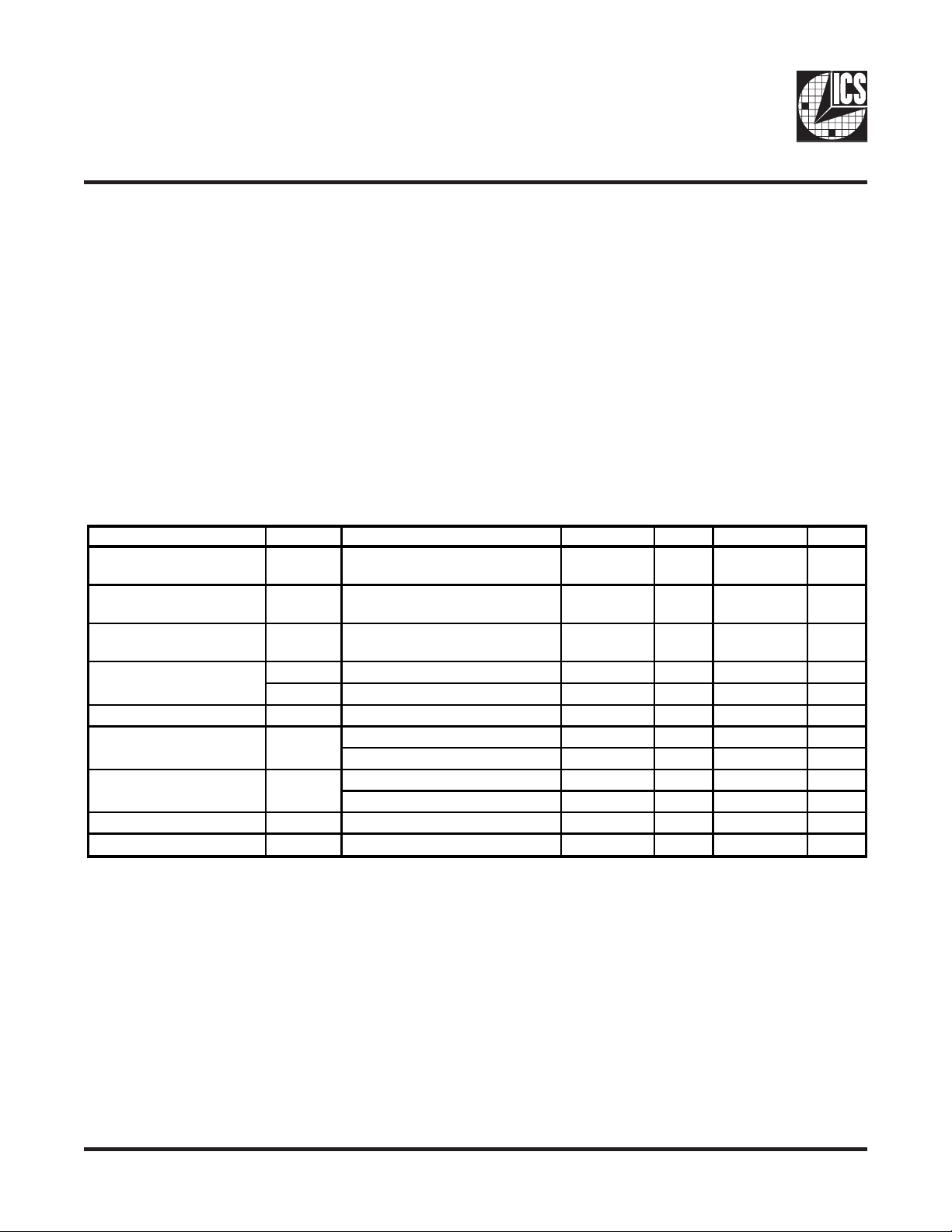
Electrical Characteristics - Input/Supply/Common Output Parameters
TA = 0 - 70°C; Supply Voltage AVDDQ, VDDQ = 1.8 V +/- 0.1V (unless otherwise stated)
1
SYMBOL
I
IH
I
IL
I
ODL
I
DD1.8
I
DDLD
V
IK
V
OH
V
OL
C
IN
C
OUT
CONDITIONS
VI = V
VI = V
OE = L, V
DDQ
DDQ
or GND
or GND
= 100mV
ODL
CL = 0pf @ 270MHz TBD
CL = 0pf
V
= 1.7V Iin = -18mA
DDQ
I
= -100 µA
OH
I
= -9 mA
OH
I
=100 µA
OL
I
=9 mA
OL
VI = GND or V
V
= GND or V
OUT
PARAMETER
Input Hi
h Current
CLK_INT, CLK_INC
Input Low Current (OE,
OS
FB_INT, FB_INC
Output Disabled Low
Current
Operating Supply
Current
Input Clamp Voltage
High-level output voltage
Low-level output voltage
In
ut Capacitance
ut Capacitance
Out
1
Guaranteed by design, not 100% tested in production.
1
DDQ
DDQ
MIN TYP MAX UNITS
±250 µA
±10 µA
100 µA
mA
V
DDQ
500
-1.2
- 0.2
µA
V
V
1.1 1.45 V
0.25 0.10 V
0.6 V
23pF
23pF
1110B—06/06/05
4
Page 5

ICS97ULP844A
(
)
Recommended Operating Condition
see note1
TA = 0 - 70°C; Supply Voltage AVDD, VDDQ = 1.8 V +/- 0.1V (unles s otherwise stated)
PARAMETER SYMBOL CONDITIONS MIN TYP MAX UNITS
Supply Voltage V
DDQ
, A
VDD
1.7 1. 8 1.9 V
CLK_INT, CLK_INC, FB_INC,
Low level input voltage V
FB_INT
IL
OE, OS 0.35 x V
High level input voltage V
DC input signal voltage
(note 2)
Differential input signal
voltage (note 3)
Output differential crossvoltage (note 4)
Input differential crossvoltage (note 4)
High level output current I
Low level output current I
Operating free-air
temperature
CLK_INT, CLK_INC, FB_INC,
FB_INT
IH
OE, OS 0.65 x V
V
IN
DC - CLK_INT, CLK_INC,
V
FB_INC, FB_INT
ID
AC - CLK_INT, CLK_INC,
FB_INC, FB_INT
V
OX
V
IX
OH
OL
T
A
0.65 x V
DDQ
DDQ
-0.3 V
0.3 V
0.6 V
V
/2 - 0.10 V
DDQ
V
/2 - 0.15 VDD/2 V
DDQ
070°C
Notes:
1. Unused inputs must be held high or low to prevent them from floating.
2. DC input signal voltage specifies the allowable DC execution of differential input.
3. Differential inputs signal voltages specifies the differential voltage [VTR-VCP]
required for switching, where VTR is the true input level and VCP is the
complementary input level.
4. Differential cross-point voltage is expected to track variations of V
and is the
DDQ
voltage at which the differential signal must be crossing.
0.35 x V
DDQ
DDQ
DDQ
DDQ
+ 0.3 V
DDQ
+ 0.4 V
DDQ
+ 0.4 V
DDQ
/2 + 0.10 V
2 + 0.15 V
-9 mA
9mA
V
V
V
V
1110B—06/06/05
5
Page 6

ICS97ULP844A
p
p
)
p
)
q
y
Timing Requirements
TA = 0 - 70°C Supply Voltage AVDD, VDDQ = 1.8 V +/- 0.1V (unless otherwise stated)
PARAMETER SYMBOL
Max clock frequency freq
Application Frequency
Range
freq
Input clock duty cycle d
op
App
tin
CONDITIONS
1.8V+ 0.1V @ 25°C
MIN TYP MAX
95 370
1.8V+ 0.1V @ 25°C 160 350
40 60
CLK stabilization T
Switching Characteristics
STAB
1
TA = 0 - 70°C Supply Voltage AVDD, VDDQ = 1.8 V +/- 0.1V (unless otherwise stated)
PARAMETER
Output enable time
Output disable time
Period jitter
Half-period jitter
Input slew rate
Out
ut clock slew rate
Cycle-to-cycle period jitter
Dynamic Phase Offset
Static Phase Offset
Output to Output Skew
SSC modulation fre
uenc
SSC clock input frequency
deviation
PLL Loop bandwidth (-3 dB
from unity gain)
SYMBOL
t
en
t
dis
t
jit (per)
t
jit(hper)
SLr1(i)
SLr1(o
t
jit(cc+)
t
jit(cc-)
t
( )dyn
2
t
SPO
t
skew
OE to any output 4.73 8 ns
OE to any output 5.82 8 ns
In
Out
CONDITION
ut Clock
ut Enable (OE), (OS
MIN TYP MAX UNITS
-30 30 ps
-60 60 ps
1 2.5 4 v/ns
0.5 v/ns
1.5 2.5 3 v/ns
040ps
0 -40 ps
-20 20 ps
-50 0 50 ps
30.00 33 kHz
0.00 -0.50 %
2.0 MHz
2.4 2.95
50 ps
Notes:
1. Switching characteristics guaranteed for application frequency range.
2. Static phase offset shifted by design.
1110B—06/06/05
6
Page 7

Y
ParameterMeasurementInformatio
n
V
DD
V
(CLKC)
ICS97ULP844
GND
V
(CLKC)
ICS97ULP844A
VDD/2
ICS97ULP844A
-VDD/2
, FB_OUTC
X
Y , FB_OUTT
X
Figure 1. IBIS Model Output Load
Z=6
C=10pF
0Ω
- GND
R=10Ω
Z = 2.97"
Z = 120Ω
Z=60Ω
R=10Ω
Z = 2.97"
C = 10 pF
GND
Figure 2. Output Load Test Circuit
t
c(n)
Z=50Ω
Z=50Ω
t
c(n+1)
V
(TT)
V
(TT)
Note: V
SCOPE
R = 1M
C = 1 pF
R = 1M
C = 1 pF
= GND
TT
Ω
Ω
t
jit(cc)=tc(n)±tc(n+1)
Figure 3. Cycle-to-Cycle Jitter
1110B—06/06/05
7
Page 8

ICS97ULP844A
CLK_INC
CLK_INT
FB_INC
FB_INT
Parameter Measurement Information
t
()n
t
()
=
n=
1
N
t
N
()n
(N is a large number of samples)
Figure 4. Static Phase Offset
t
( ) n+1
Y
X
Y
Y , FB_OUTC
X
Y , FB_OUTT
X
Y , FB_OUTC
X
Y , FB_OUTT
X
Y , FB_OUTC
X
Y , FB_OUTT
X
#
X
t
(skew)
Figure 5. Output
t
C(n)
Skew
1
f
O
t
=
(jit_per)tc(n)
1
-
f
O
1110B—06/06/05
Figure 6. Period Jitter
8
Page 9

ICS97ULP844A
Y , FB_OUTC
X
Y , FB_OUTT
X
Clock Inputs
and Outputs
20%
Parameter Measurement
t
jit(hper_n)
1
f
o
t
t
=-
jit(hper)
jit(hper_n)
Figure 7. Half-Period Jitter
80%
t
slr
Information
t
jit(hper_n+1)
1
2xf
O
t
slf
80%
20%
VID,V
OD
1110B—06/06/05
Figure 8. Input and Output Slew Rates
9
Page 10

ICS97ULP844A
CK
CK
FBIN
FBI
N
t
( )dyn
OE
Y/ Y
OE
t
( )
SSC OFF
SSC ON SSC ON
t
( )dyn
t
( )dyn
SSC OFF
t
( )
t
( )dyn
Figure 9. Dynamic Phase Off set
50% VDDQ
t
en
Y
50% VDDQ
Y
% VDDQ
50
t
Y
dis
1110B—06/06/05
50 % VD
DQ
Y
Figure 10. Time delay between OE and Clock Output (Y,
10
Y)
Page 11

ICS97ULP844A
Figure 11. AVDD Filtering
- Place the 2200pF capacitor close to the PLL.
- Use a wide trace for the PLL analog power & ground. Connect PLL & caps to AGND trace & connect trace to one
GND via (farthest from PLL).
- Recommended bead: Fair-Rite P/N 2506036017Y0 or equivalent (0.8 Ohm DC max, 600 Ohms @ 100 MHz).
1110B—06/06/05
11
Page 12

ICS97ULP844A
SYMBOL
A 0.80 0.90 1.00 0.031 0.035 0.039
A1 0.165 0.20 0.235 0.006 0.008 0.009
A2 0.16 0.20 0.24 0.006 0.008 0.009
A3 0.475 0.50 0.525 0.019 0.020 0.021
b 0.35 0.40 0.45 0.014 0.016 0.018
D 3.90 4.00 4.10 0.154 0.157 0.161
D1
E 4.40 4.50 4.60 0.173 0.177 0.181
E1
e
Ordering Information
ICS97ULP844AH(LF)-T
Example:
ICS XXXX y H (LF)- T
Millimeter Inch
MIN NOM MAX MIN NOM MAX
0.102 BSC2.60 BSC
3.25 BSC
0.65 BSC
Designation for tape and reel packaging
RoHS Compliant (Optional)
Package Type
H = BGA
Revision Designator (will not correlate with datasheet revision)
Device Type
Prefix
ICS = Standard Device
0.128 BSC
0.026 BSC
1110B—06/06/05
12
 Loading...