

Page 1
查询ICS95V847YGLF-T供应商
Integrated
ICS95V847
Circuit
Systems, Inc.
2.5V Wide Range Frequency Clock Driver (45MHz - 233MHz)
Recommended Application:
• Zero Delay Board Fan Out, SO-DIMM
• Provides complete DDR registered DIMM solution
with ICSSSTV16857, ICSSSTV16859 or
ICSSSTV32852
Product Description/Features:
• Low skew, low jitter PLL clock driver
• 1 to 5 differential clock distribution (SSTL_2)
• Feedback pins for input to output synchronization
• Spread Spectrum tolerant inputs
Switching Characteristics:
• CYCLE - CYCLE jitter: <60ps
• OUTPUT - OUTPUT skew: <60ps
• Period jitter: ±30ps
• DUTY CYCLE: 49.5% - 50.5%
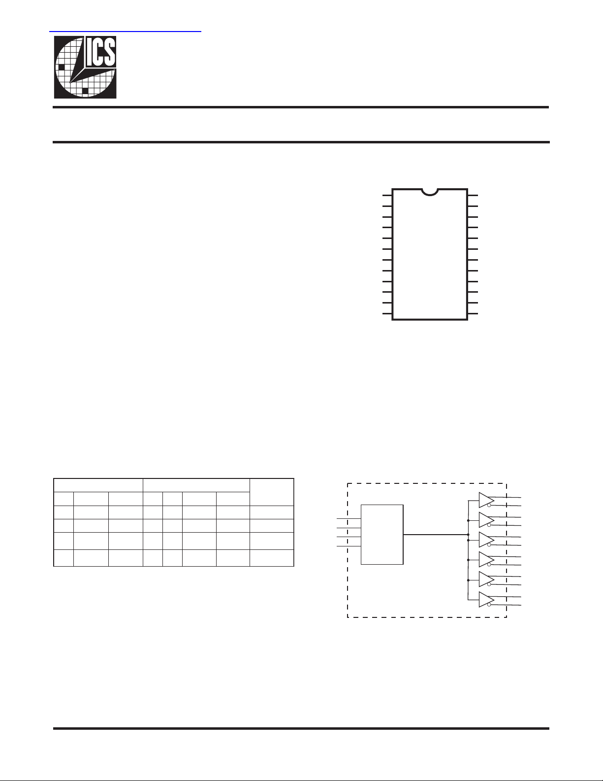
Pin Configuration
GND
CLKC0
CLKT0
GND
VDD
CLK_INT
CLK_INC
AVD D
AGND
CLKC1
CLKT1
VDD
4.40 mm. Body, 0.65 mm. pitch
1
2
3
4
5
6
7
8
9
10
11
12
24
23
22
21
20
847
19
18
17
ICS95V
16
15
14
13
24-Pin TSSOP
CLKT4
CLKC4
CLKC3
CLKT3
VDD
FB_INT
FB_INC
FB_OUTC
FB_OUTT
CLKT2
CLKC2
GND
Functionality
STUPNISTUPTUO
DDVATNI_KLCCNI_KLCTKLCCKLCTTUO_BFCTUO_BF
DNGL HLHL H ffo/dessapyB
DNGH LHLH L ffo/dessapyB
V5.2
LHLHLH no
)mon(
V5.2
HLHLHL no
)mon
(
0718D—04/08/05
Block Diagram
etatSLLP
FB_INT
FB_INC
CLK_INC
CLK_INT
PLL
FB_OUTT
FB_OUTC
CLKT0
CLKC0
CLKT1
CLKC1
CLKT2
CLKC2
CLKT3
CLKC3
CLKT4
CLKC4
Page 2

ICS95V847
Pin Descriptions
REBMUNNIPEMANNIPEPYTNOITPIRCSED
02,21,5DDVRWPV5.2,ylppusrewoP
31,4,1DNGRWPdnuorG
8DDVARWPV5.2,ylppusrewopgolanA
9DNGARW
42,12,51,11,3]4:0[TKLCTUOstuptuoriaplaitnereffidfokcolC"eurT"
PdnuorggolanA
32,22,41,01,2]4:0[CKLCTUOstuptuori
6TNI_KLCNItupnikcolcecnerefer"eurT"
7CNI_KLCNItupnikcolcecnerefer"yratn
61TTUO_BFTUO
71CTUO_BFTUO
91TNI_BFNI
81CNI_BFNI
emelpmoC"
TNI_BF
pmoC"
CNI_BFot
aplaitnereffidfoskcolc"yratnemelpmoC"
sehctiwstI.kcabdeeflanretxerofdetacided,tuptuokcabdeeF""eurT"
hT.KLCehtsaycneuqerfemasehtta
skcabdeefsedivorp,tupnikcabdeeF"eurT"
rorreesahpetanimileotTNI_KLChtiwnoitazinorhcnys
otderiwebtsumtuptuosi
tI.kcabdeeflanretxerofdetacided,tuptuokcabdeeF"yratnemel
deriwebtsumtuptuosihT.KLCehtsaycneuqerfemasehttasehctiws
rofLLPlanretniehtotlangi
niehtotlangissedivorp,tupnikcabdeeF"yratnemelpmoC"
rorreesahpetanimileotCNI_KLChtiwnoitazinorhcnysrof
LLPlanret
This PLL Clock Buffer is designed for a VDD of 2.5V, an AVDD of 2.5V and differential data input and output levels.
ICS95V847 is a zero delay buffer that distributes a differential clock input pair (CLK_INT, CLK_INC) to five differential
pair of clock outputs (CLKT[4:0], CLKC[4:0]) and one differential pair feedback clock output (FB_OUT, FB_OUTC). The
clock outputs are controlled by input clock (CLK_INT, CLK_INC), the feedback clock (FB_INT, FB_INC) and the analog
power input (AVDD). When AVDD is grounded, the PLL is turned off and bypassed for test purposes.
The PLL in ICS95V847 clock driver uses the input clock (CLK_INC, CLK_INT) and the feedback clock (FB_INT,
FB_INC) to provide high-performance, low-skew, low-jitter differential output clocks (CLKT[4:0], CLKC[4:0]). ICS95V847
is also able to track Spread Spectrum Clock (SSC) for reduced EMI.
ICS95V847 is characterized for operation from 0°C to 85°C.
0718D—04/08/05
2
Page 3
Absolute Maximum Ratings
p
Supply Voltage (VDD & AVDD). . . . . . . . . . . -0.5V to 4.6V
Logic Inputs . . . . . . . . . . . . . . . . . . . . . . . . . GND - 0.5V to VDD + 0.5V
Ambient Operating Temperature . . . . . . . . . . 0°C to +85°C
Storage Temperature . . . . . . . . . . . . . . . . . . . -65°C to +150°C
ICS95V847
Stresses above those listed under
Absolute Maximum Ratings
may cause permanent damage to the device. These
ratings are stress specifications only and functional operation of the device at these or any other conditions above those
listed in the operational sections of the specifications is not implied. Exposure to absolute maximum rating conditions
for extended periods may affect product reliability.
Electrical Characteristics - Input/Supply/Common Output Parameters
TA = 0 - 85°C; Supply Voltage A
PARAMETER SYMBOL CONDITIONS MIN TYP MAX UNITS
Input High Current I
Input Low Current I
Operating Supply
Current
I
DD2. 5
I
High Impedance
ut Current
Out
Input Clamp Voltage V
High-level output
voltage
V
Low-level output voltage V
Input Capacitance
1
Guaranteed by design at 233MHz, not 100% tested in production.
1
IH
IL
DDPD
I
OZ
IK
OH
OL
C
IN
, VDD = 2.5 V +/- 0.2V (unless otherwise stated)
VDD
VI = VDD or GND 5 µA
VI = VDD or GND 5 µA
CL = 0pf @ 200MHz 148 mA
CL = 0pf 100 µA
V
= 2.7V, Vout = VDD or
DD
GND
±10 mA
VDD = 2.3V Iin = -18mA -1.2
= -1 mA VDD - 0.1 V
I
OH
I
= -12 mA 1.7V V
OH
I
=1 mA 0.1 V
OL
I
=12 mA 0.6 V
OH
VI = GND or V
DD
2.5 3.5 pF
V
0718D—04/08/05
3
Page 4

ICS95V847
(
)
-
Recommended Operating Condition
see note1
TA = 0 - 85°C; Supply Voltage AVDD, VDD = 2.5 V +/- 0.2V (unless otherwise stated)
PARAMETER SYMBOL CONDITIONS MIN TYP MAX UNITS
Supply Voltage V
DD
Low level input voltage V
High level input voltage V
DC input signal voltage
(note 2)
Differential input signal
voltage (note 3)
Output differential cross
voltage (note 4)
V
Input differential crossvoltage (note 4)
High level output
current
Low level output current I
Operating free-air
temperature
, A
V
V
V
I
T
OX
OH
OL
VDD
CLKT, CLKC, FB_INC 0.4 V
IL
PD# -0.3 0.7 V
CLKT, CLKC, FB_INC V
IH
IN
PD# 1.7 V
DC - CLKT, FB_INT 0.36 V
ID
IX
AC - CLKT, FB_INT 0.7 V
A
2.3 2.5 2.7 V
/2 - 0.18 V
DD
/2 + 0.18 2.1 V
DD
+ 0.6 V
DD
-0.3 V
+ 0.3 V
DD
+ 0.6 V
DD
+ 0.6 V
DD
VDD/2 - 0.15 VDD/2 + 0.15 V
VDD/2 - 0.2 VDD/2 VDD/2 + 0.2 V
-6.4 mA
5.5 mA
085°C
Notes:
1. Unused inputs must be held high or low to prevent them from floating.
2. DC input signal voltage specifies the allowable DC execution of differential input.
3. Differential inputs signal voltages specifies the differential voltage [VTR-VCP]
required for switching, where VT is the true input level and VCP is the
complementary input level.
4. Differential cross-point voltage is expected to track variations of VDD and is the
voltage at which the differential signal must be crossing.
0718D—04/08/05
4
Page 5

Timing Requirements
j
)
)
)
(p
)
TA = 0 - 85°C; Supply Voltage A
PARAMETER SYMBOL
Max clock frequency freq
Application Frequency
Range
Input clock duty cycle d
, VDD = 2.5 V +/- 0.2V (unless otherwise stated)
VDD
freq
tin
op
App
CONDITIONS
2.5V+0.2V @ 25oC
2.5V+0.2V @ 25oC
ICS95V847
MIN MAX UNITS
45 233 MHz
95 210 MHz
40 60 %
CLK stabilization T
STAB
15 µs
Switching Characteristics (see note 3)
PARAMETER SYMBOL CONDITION MIN TYP MAX UNITS
Low-to high level
propagation delay time
High-to low level propagation
delay time
Output enable time t
Output disable time tdis PD# to any output 5 ns
Period jitter T
Half-period jitter t(jit_hper) 100MHz to 200MHz -75 30 ps
Input clock slew rate t
Output clock slew rate t
Cycle to Cycle Jitter
1
Phase error
Output to Output Skew T
Notes:
1. Refers to transition on noninverting output in PLL bypass mode.
2. While the pulse skew is almost constant over frequency, the duty cycle error
increases at higher frequencies. This is due to the formula: duty cycle=twH/tc, where
the cycle (tc) decreases as the frequency goes up.
3. Switching characteristics guaranteed for application frequency range.
4. Static phase offset shifted by design.
t
t
T
cyc-Tcyc
t
hase error
PLH
PLL
EN
it (per
sl(i
sl(o
skew
1
1
CLK_IN to any output 5.5 ns
CLK_IN to any output 5.5 ns
PD# to any output 5 ns
100MHz to 200MHz -30 30 ps
14V/ns
12.5V/ns
100MHz to 200MHz 60 ps
4
-50 0 50 ps
60 ps
0718D—04/08/05
5
Page 6

ICS95V847
Parameter Measurement Information
V
DD
V
(CLKC)
R=60Ω
VDD/2
ICS95V847
ICS95V847
GND
Figure 1. IBIS Model Output Load
C=14pF
Z=60Ω
Z=60Ω
-VDD/2
R=10Ω
R=10Ω
C=14pF
R=60Ω
V
(CLKC)
Z=50Ω
Z=50Ω
VDD/2
V
SCOPE
R=50Ω
(TT)
R=50Ω
V
(TT)
0718D—04/08/05
-VDD/2
NOTE: V
Y , FBOUTC
X
Y , FBOUTT
X
(TT)
=
GND
-VDD/2
Figure 2. Output Load Test Circuit
t
c(n)
t
jit(cc)=tc(n)±tc(n+1)
Figure 3. Cycle-to-Cycle Jitter
6
t
c(n+1)
Page 7

CLK_INC
CLK_INT
FB_INC
FB_INT
Parameter Measurement Information
t
()n
t
()
=
n=
1
N
t
N
()n
(N is a large number of samples)
Figure 4. Static Phase Offset
ICS95V847
t
( ) n+1
Y
X
Y
Y , FB_OUTC
X
Y , FB_OUTT
X
Y , FB_OUTC
X
Y , FB_OUTT
X
Y , FB_OUTC
X
Y , FB_OUTT
X
#
X
t
(SK_O)
Figure 5. Output
Skew
1
f
O
t
=t-
(jit_per) C(n)
1
f
O
0718D—04/08/05
Figure 6. Period Jitter
7
Page 8

ICS95V847
Y , FB_OUTC
X
Y , FB_OUTT
X
Clock Inputs
and Outputs
20%
Parameter Measurement
t
(hper_n)
t
(jit_Hper)t(jit_Hper_n)
=-
Figure 7. Half-Period Jitter
80%
Rise t
sl
1
f
o
Information
t
(hper_n+1)
1
2xf
O
Fall t
sl
80%
20%
VID,V
OD
0718D—04/08/05
Figure 8. Input and Output Slew Rates
8
Page 9

ICS95V847
INDEX
AREA
1 2
SEATING
PLANE
- C -
N
E1
INDEX
AREA
12
D
A2
e
b
E
A
A1
aaa
4.40 mm. Body , 0.65 mm. pitch TSSOP
(173 mil)
(0.0256 Inch)
c
-C-
SEATING
PLANE
C
In Millimeters In Inches
SYMBOL
L
COMMON DIMENSIONS COMMON DIMENSIONS
MIN MAX MIN MAX
A -- 1.20 -- .047
A1 0.05 0.15 .002 .006
A2 0.80 1.05 .032 .041
b 0.19 0.30 .007 .012
c 0.09 0.20 .0035 .008
D
E
α
E1 4.30 4.50 .169 .177
e
SEE VARIATIONS SEE VARIATIONS
6.40 BASIC 0.252 BASIC
0.65 BASIC 0.0256 BASIC
L 0.45 0.75 .018 .030
N
SEE VARIATIONS SEE VARIATIONS
a0°8°0°8°
aaa -- 0.10 -- .004
VARIATIONS
N
D mm. D (inch)
MIN MAX MIN MAX
24 7.70 7.90 .303 .311
Reference Doc.: J EDEC Publication 95, MO-153
10-0035
Ordering Information
ICS95V847yGLF-T
Example:
ICS XXXX y G LF- T
0718D—04/08/05
Designation for tape and reel packaging
Annealed Lead Free (Optional)
Package Type
G = TSSOP
Revision Designator (will not correlate with datasheet revision)
Device Type
Prefix
ICS = Standard Device
9
 Loading...