

Page 1
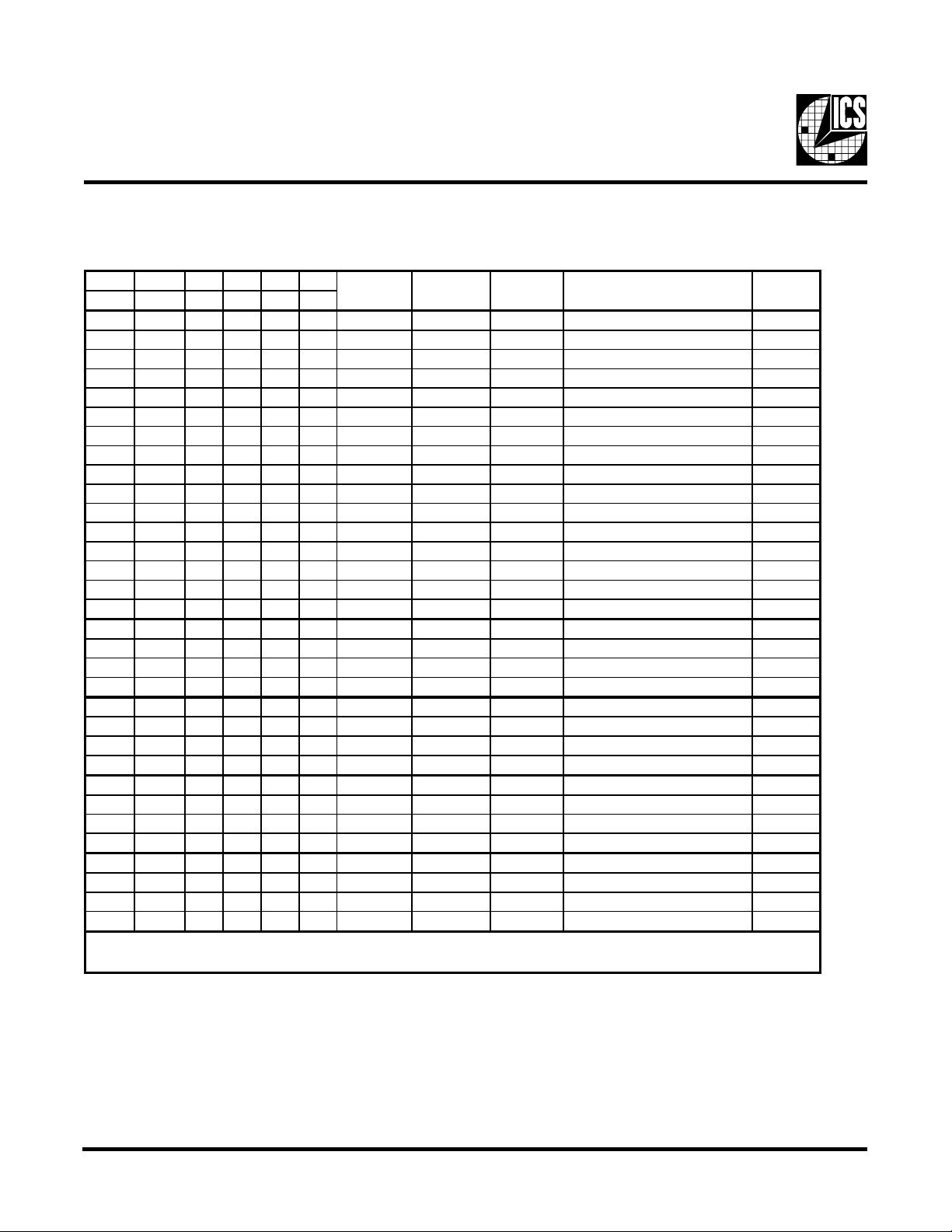
VDDREF
GND
X1
X2
AVDD48
*FS2/48MHz
*FS3/24_48MHz
GND
*WDEN/PCICLK_F
*SEL24_48#/PCICLK0
PCICLK1
GND
PCICLK2
PCICLK3
VDDPCI
PCICLK4
PCICLK5
PCICLK6
GND
PCICLK7
PCILCK8
PCICLK9_E
VDDPCI
SRESET#
REF0/
REF1/FS1*
REF_F
RATIO
AGP_STOP#*
GND
CPUCLKT0
CPUCLKC0
VDDL
CPUCLK_CST0
CPUCLK_CSC0
GND
CPU_STOP#*
PCI_STOP#*
PD#*
AVDD
AGND
S DATA
SCLK
GND
AGP2
AGP1
AGP0
VDDAGP
FS0*
ICS94229
1
2
3
4
5
6
7
8
9
10
11
12
13
14
15
16
17
18
19
20
21
22
23
24
48
47
46
45
44
43
42
41
40
39
38
37
36
35
34
33
32
31
30
29
28
27
26
25
查询ICS94229供应商
Integrated
ICS94229
Circuit
Systems, Inc.
Advance Information
Programmable System Clock Chip for AMD - K7™ processor
Recommended Application:
VIA KT266 style chipset
Output Features:
• 1 - Differential pair open drain CPU clocks @ 2.5V
• 1 - Differential pair push-pull CPU clocks @ 2.5V
• 11 - PCI including 1 free running and 1 early @ 3.3V
• 1 - 48MHz, @ 3.3V fixed
• 1 - 24/48MHz @ 3.3V
• 3 - REF @ 3.3V, 14.318MHz.
Features:
• Programmable output frequency.
• Programmable output rise/fall time.
• Programmable slew and skew control for CPUCLK,
PCICLK, AGP, REF, 48MHz and 24_48MHz.
• Real time system reset output.
• Spread spectrum for EMI control typically
by 7dB to 8dB, with programmable spread percentage.
• Watchdog timer technology to reset system
if over-clocking causes malfunction.
• Uses external 14.318MHz crystal.
Skew Specifications:
• CPU - CPU: <175ps
• PCI - PCI: <500ps
• CPU (early - PCI: min=1.0ns, max=2.0ns
• CPU cycle to cycle jitter: <250ps
* Internal Pull-up Resistor of 120K to VDD
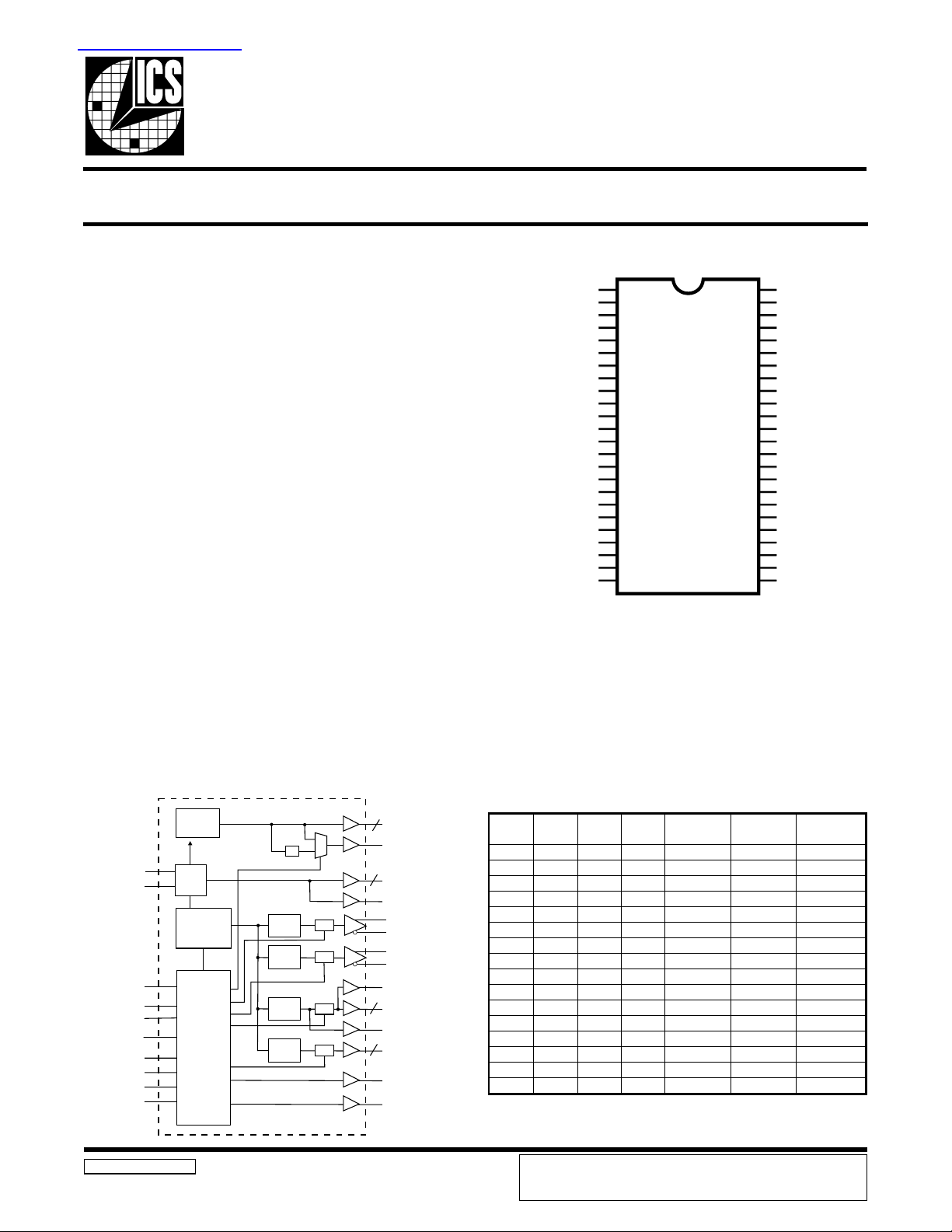
Pin Configuration
48-Pin 300mil SSOP
Block Diagram
SEL24_48#
PCI_STOP#
CPU_STOP#
AGP_STOP#
94229 Rev - 05/31/01
Third party brands and names are the property of their respective owners.
X2
S DATA
SCLK
FS (3:0)
PD#
Functionality
PLL2
/ 2
X1
XTAL
OSC
PLL1
Spread
Spectrum
Control
Logic
Config.
Reg.
CPU
DIVDER
CPU
DIVDER
PCI
DIVDER
AGP
DIVDER
Stop
Stop
Stop
Stop
48MHz (1:0)
2
24_48MHz
REF (1:0)
2
REF_F
CPUCLKT0
CPUCLKC0
CPUCLK_CST0
CPUCLK_CSC0
PCICLK9_E
PCICLK (8:0)
9
PCICLK_F
AGP (2:0)
3
SRESET#
RATIO
3SF2SF1SF0SF
0000 33.33287.7788.83
0001 00.02233.3776.63
0010 00.01200.0700.53
0011 00.00276.6633.33
0100 00.09100.6700.83
0101 00.08100.2700.63
0110 00.07100.8600.43
0111 00.05100.5705.73
1000 00.04100.0700.53
100 1 00.02100.0600.03
1010 00.01100.6600.33
1011 76.6676.6633.33
1100 00.00276.6633.33
1101 76.66176.6633.33
1110 00.00176.6633.33
1111 33.33176.6633.33
ADVANCE INFORMATION documents contain information on products
in the formative or design phase development. Characteristic data and
other specifications are design goals. ICS reserves the right to change or
discontinue these products without notice.
UPC
)zHM(
PGA
)zHM(
KLCICP
)zHM(
Page 2
ICS94229
Advance Information
Pin Descriptions
REBMUNNIPEMANNIPEPYTNOITPIRCSED
,52,32,51,1DDVRWPV3.3lanimon,ylppusrewoP
,91,21,8,2
34,73,92
31XNI 2Xmorfrotsiserkcabdeefdna)Fp63(pacdaollanretnisah,tupnilatsyrC
42XTUO)Fp63(pacdaollanretnisaH.zHM813.41yllanimon,tuptuolatsyrC
584DDVARWPV3.3lanimon,ylppusrewoP
6
7
9
01
11,31,41,61
22E_9KLCICPTUO .#POTS_ICPybdeppotsebnaC.sn2ybskcolcICPlarenegsdaeL.kcolcICPylraE
42#TESERS
62,72,82)0:2(PGATUOstuptuokcolcPGA
03KLCSNIIfotupnikcolC
13ATADSO/IIrofnipataD
23DNGARWPdnuorggolanA
33DDVARWPV3.3lanimon,ylppusrewoP
43#DPNI
53#POTS_ICPNI woltupninehw,level0cigoltaskcolcF_KLCICPehtsedisebsKLCICPllaspotS
63#POTS_UPC
830CSC_KLCUPCTUO
930TSC_KLCUPCTUO
04LDDVRWPV5.2lanimon,sKLCUPCrofylppusrewoP
240TKLCUPCTUO
140CKLCUPCTUO
44#POTS_PGANIwoltupninehw,level0cigoltaskcolcPGAllaspotS
54
64F_FERTUO#POTS_FERybdetcetffaton,.kcolcecnerefergninnureerfzHM813.41
74
84
DNGRWPdnuorG
2,1
2SF
zHM84TUOkcolctuptuozHM84
2,1
3SF
zHM84_42TUOtuptuokcolczHM84ro42
NEDWNI .zHM001siycneuqerfefastluafeD.tiucricgodhctawfoelbaneerawdraH
F_KLCICPTUO .tnemeganamrewoprof#POTS_ICPybdetceffatonkcolcICPgninnureerF
#84_42LES
0KLCICPTUOtuptuokcolcICP
,71,81,02,12
1
OITARTUOegdirBhtuoSehtotzHM331rof"1"rozHM001rof"0"astuptuO
2,1
1SF
1FERTUO.kcolcecnereferzHM813.41
2,1
0SF
0FERTUO.kcolcecnereferzHM813.41
2,1
)1:8(KLCICPTUO.stuptuokcolcICP
2,1
NItupnIdehctaL.niptcelesycneuqerF
NItupnIdehctaL.niptcelesycneuqerF
NItuptuo7niprofzHM84ro42tcelesottupnicigoL
TUO .wolevitcasilangissihT.tuoemitremtgodhctawroflangistesermetsysemitlaeR
NI
NItupnIdehctaL.niptcelesycneuqerF
NItupnIdehctaL.niptcelesycneuqerF
2
2
tupnitnarelotV5,tupniC
tnarelotV5yrtiucricC
rewopwolaotniecivedehtnwodrewopotdesuniptupniwolevitcasuonorhcnysA
ehT.deppotseralatsyrcehtdnaOCVehtdnadelbasideraskcolclanretniehT.etats
.sm3nahtretaergebtonlliwnwodrewopehtfoycnetal
"0"cigoltaskcolcSC_CKLCUC&CKLCUPC,TKLCUPCstlahtupnisuonorhcnysasihT
.wolnevirdnehwlevel
nadeenstuptuollup-hsupesehT.tuptuoUPCriaplaitnereffidfokcolc"yratnemelpmoC"
)llup-hsup(pu-llupV5.1lanretxe
V5.1lanretxenadeenstuptuollup-hsupesehT.tuptuoUPCriaplaitnereffidfokcolc"eurT"
.)llup-hsup(pu-llup
V5.1lanretxenadeenstuptuoniardnepoesehT.tuptuoUPCriaplaitnereffidfokcolc"eurT"
.)niardnepo(pu-llup
nadeenstuptuoniardnepoesehT.tuptuoUPCriaplaitnereffidfokcolc"yratnemelpmoC"
.)niardnepo(pu-llupV5.1lanretxe
Notes:
1: Internal Pull-up Resistor of 120K to 3.3V on indicated inputs
2: Bidirectional input/output pins, input logic levels are latched at internal power-on-reset. Use 10Kohm resistor
to program logic Hi to VDD or GND for logic low.
Third party brands and names are the property of their respective owners.
2
Page 3

ICS94229
Advance Information
General Description
The ICS94229 is a main clock synthesizer chip for AMD-K7 based systems with VIA KT266 style chipset. This provides all
clocks required for such a system.
The ICS94229 belongs to ICS new generation of programmable system clock generators. It employs serial programming I2C
interface as a vehicle for changing output functions, changing output frequency, configuring output strength, configuring
output to output skew, changing spread spectrum amount, changing group divider ratio and dis/enabling individual clocks.
This device also has ICS propriety 'Watchdog Timer' technology which will reset the frequency to a safe setting if the system
become unstable from over clocking.
SRESET# Signal Description
The SRESET# signal from ICS94229 system clock generator is a real time active low pulse that can be used to reset the system.
The Open-Drain Nch output Reset# pin needs to be tied to the system reset line which has a pull-up resistor. When activated,
the SRESET# output will be driven to a low with a 288ms pulse width.
Third party brands and names are the property of their respective owners.
3
Page 4
ICS94229
Advance Information
General I2C serial interface information
How to Write:
• Controller (host) sends a start bit.
• Controller (host) sends the write address D2
• ICS clock will acknowledge
• Controller (host) sends a dummy command code
• ICS clock will acknowledge
• Controller (host) sends a dummy byte count
• ICS clock will acknowledge
• Controller (host) starts sending Byte 0 through Byte 16
(see Note 2)
• ICS clock will acknowledge each byte one at a time
• Controller (host) sends a Stop bit
How to Write:
Controll e r (Host)
Start Bit
Address D2
Dummy Command Code
Dummy Byte Count
(H)
Byte 0
Byte 1
Byte 2
Byte 3
Byte 4
Byte 5
Byte 6
ICS (Slave/Receiver)
(H)
ACK
ACK
ACK
ACK
ACK
ACK
ACK
ACK
ACK
ACK
How to Read:
• Controller (host) will send start bit.
• Controller (host) sends the read address D3
• ICS clock will acknowledge
• ICS clock will send the byte count
• Controller (host) acknowledges
• ICS clock sends Byte 0 through byte 6 (default)
• ICS clock sends Byte 0 through byte X (if X
written to byte 6).
• Controller (host) will need to acknowledge each byte
• Controller (host) will send a stop bit
H ow to Read:
Controlle r (Host)
Start B it
Addres s D3
ACK
ACK
ACK
ACK
ACK
ACK
ACK
ACK
If 7
has been wri t ten to B 6
H
ACK
(H)
ICS (Slave/Receiver)
ACK
Byte Count
Byte 0
Byte 1
Byte 2
Byte 3
Byte 4
Byte 5
Byte 6
Byte 7
(H)
(H)
was
Byte 14
ACK
Byte 15
ACK
Byte 16
ACK
Stop Bit
*See notes on the following page.
Third party brands and names are the property of their respective owners.
If 1A
has been wri t ten to B 6
H
ACK
If 1B
has been wri t ten to B 6
H
ACK
has been wri t ten to B 6
If 1C
H
ACK
St op Bit
Byte 14
Byte 15
Byte 16
4
Page 5
Advance Information
g
Brief I2C registers description for
Programmable System Frequency Generator
Register Name Byte Description PWD Default
Functionality & F requency
Select Register
Output Control Registers 1, 2, 3
Vendor ID & Revision ID
Registers
Byte Count
Read B ack Register
Watchdog Enable Register 4
Watchdog Control Registers
VCO Con trol Selectio n Bit 4, 5
VCO Frequency Control
Registers
Spread Spectrum Control
Registers
Group Skews Control
Registers
Output Rise/Fall Time
Select Registers
0
5, 6, 7
8
9, 10
11, 12
13, 14
15, 16
Output frequency, hardware / I
frequency s elect, spread spectrum &
output enable control register.
Active / inactive outpu t control
registers/latch inputs read back.
Byte 11 bit[7:4] is ICS vendor id - 1001.
Other bits in this register designate device
revision ID of this part.
Writing to this regis ter w ill con figu re
byte count and how many b yte w ill be
read back. Do not write 00
Writing to this regis ter w ill con figu re the
number of seconds for the watchdog
timer to res et.
Watchdog enable, watchdog status and
programmable 'safe' frequency' can be
confi
ured in th is register .
This bit s elect w hether the outp ut
frequency is control by hardware/byte 0
configurations or byte 11&12
programming.
Thes e registers control the dividers ratio
into the phase detector and thus control
the VCO output frequency.
Thes e registers control the spread
percentage amount.
Increment or d ecrement the group skew
amount as compared to the initial skew.
These registers will control the output
ris e and fall time.
2
C
to this byte.
H
See individual
byte description
See individual
byte description
See individual
byte description
000,0000
Depended on
hardware/byte 0
con figuration
Depended on
hardware/byte 0
con figuration
See individual
byte description
See individual
byte description
ICS94229
08
H
10
H
0
Notes:
1. The ICS clock generator is a slave/receiver, I2C component. It can read back the data stored in the latches for
verification. Readback will support standard SMBUS controller protocol. The number of bytes to readback is
defined by writing to byte 8.
2. When writing to byte 11 - 12, and byte 13 - 14, they must be written as a set. If for example, only byte 14 is written
but not 15, neither byte 14 or 15 will load into the receiver.
3. The data transfer rate supported by this clock generator is 100K bits/sec or less (standard mode)
4. The input is operating at 3.3V logic levels.
5. The data byte format is 8 bit bytes.
6. To simplify the clock generator I
bytes must be accessed in sequential order from lowest to highest byte with the ability to stop after any complete
byte has been transferred. The Command code and Byte count shown above must be sent, but the data is ignored
for those two bytes. The data is loaded until a Stop sequence is issued.
7. At power-on, all registers are set to a default condition, as shown.
Third party brands and names are the property of their respective owners.
2
C interface, the protocol is set to use only Block-Writes from the controller. The
5
Page 6
ICS94229
Advance Information
Serial Configuration Command Bitmap
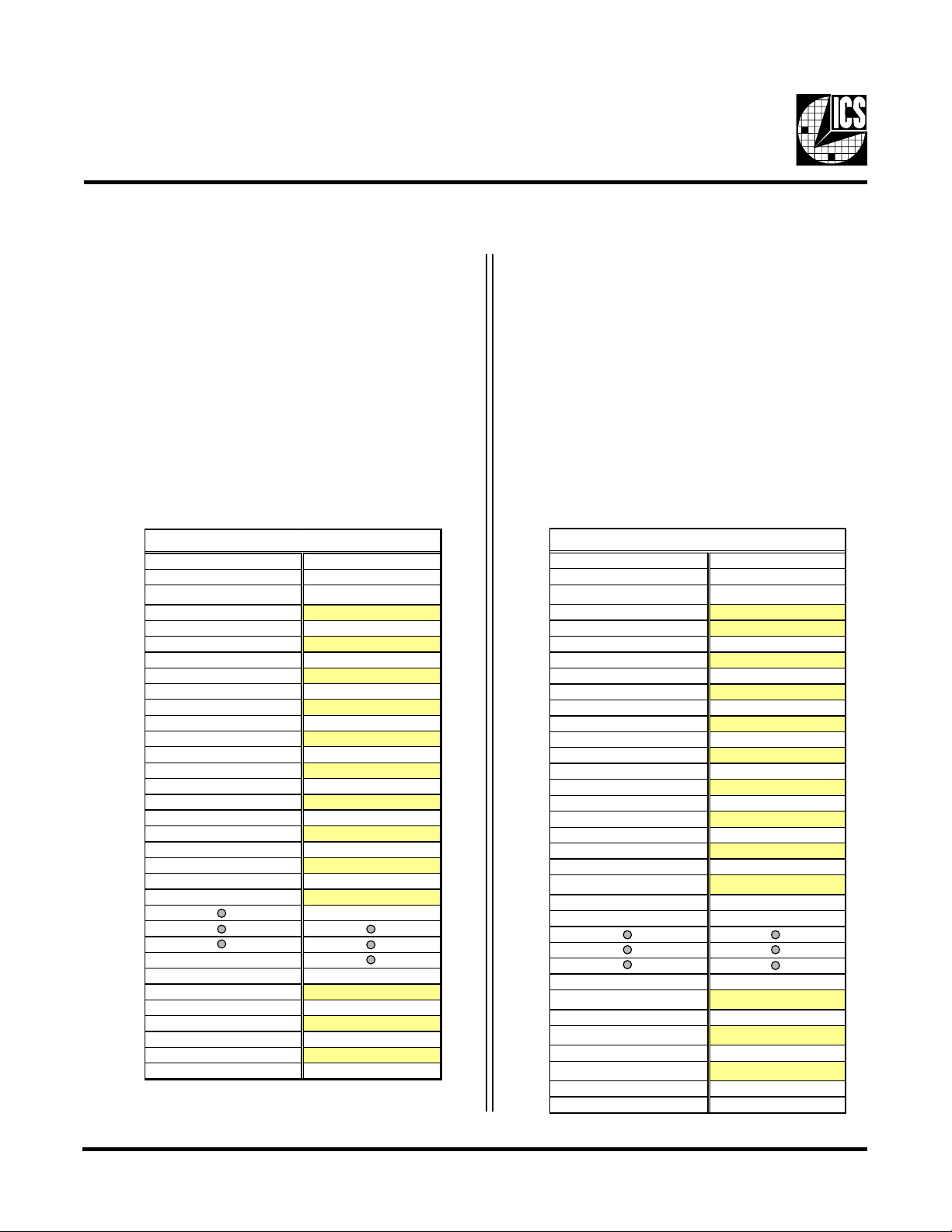
Byte0: Functionality and Frequency Select Register (default = 0)
Bit5 Bit4 Bit3 Bit2 Bit1 Bit0
SSB1 SSB0 FS3 FS2 FS1 FS0
0 0 0 0 0 0 233.33 77. 78 38.88 +/- 0. 25% Cent er Spread N/ A
0 0 0 0 0 1 220.00 73. 33 36.67 +/- 0. 25% Cent er Spread N/ A
0 0 0 0 1 0 210.00 70. 00 35.00 +/- 0. 25% Cent er Spread N/ A
0 0 0 0 1 1 200.00 66. 67 33.33 +/- 0. 25% Cent er Spread N/ A
0 0 0 1 0 0 190.00 76. 00 38.00 +/- 0. 25% Cent er Spread N/ A
0 0 0 1 0 1 180.00 72. 00 36.00 +/- 0. 25% Cent er Spread N/ A
0 0 0 1 1 0 170.00 68. 00 34.00 +/- 0. 25% Cent er Spread N/ A
0 0 0 1 1 1 150.00 75. 00 37.50 +/- 0. 25% Cent er Spread N/ A
0 0 1 0 0 0 140.00 70. 00 35.00 +/- 0. 25% Cent er Spread N/ A
0 0 1 0 0 1 120.00 60. 00 30.00 +/- 0. 25% Cent er Spread N/ A
0 0 1 0 1 0 110.00 66. 00 33.00 +/- 0. 25% Cent er Spread N/ A
0 0 1 0 1 1 66.67 66.67 33. 33 +/- 0.25% Center S pread N/A
0 0 1 1 0 0 200.00 66. 67 33.33 +/- 0. 25% Cent er Spread N/ A
0 0 1 1 0 1 166.67 66. 67 33.33 +/- 0. 25% Cent er Spread N/ A
0 0 1 1 1 0 100.00 66. 67 33.33 +/- 0. 25% Cent er Spread 0
0 0 1 1 1 1 133.33 66. 67 33.33 +/- 0. 25% Cent er Spread 1
1 0 0 0 0 0 200.00 66. 67 33.33 0 to -0.5% Down S pread N/A
1 0 0 0 0 1 166.67 66. 67 33.33 0 to -0.5% Down S pread N/A
1 0 0 0 1 0 100.00 66. 67 33.33 0 to -0.5% Down S pread 0
1 0 0 0 1 1 133.33 66. 67 33.33 0 to -0.5% Down S pread 1
1 0 0 1 0 0 200.00 66. 67 33.33 +/- 0. 50% Cent er Spread N/ A
1 0 0 1 0 1 166.67 66. 67 33.33 +/- 0. 50% Cent er Spread N/ A
1 0 0 1 1 0 100.00 66. 67 33.33 +/- 0. 50% Cent er Spread 0
1 0 0 1 1 1 133.33 66. 67 33.33 +/- 0. 50% Cent er Spread 1
1 1 1 0 0 0 200.00 66. 67 33.33 +/- 0. 75% Cent er Spread N/ A
1 1 1 0 0 1 166.67 66. 67 33.33 +/- 0. 75% Cent er Spread N/ A
1 1 1 0 1 0 100.00 66. 67 33.33 +/- 0. 75% Cent er Spread 0
1 1 1 0 1 1 133.33 66. 67 33.33 +/- 0. 75% Cent er Spread 1
1 1 1 1 0 0 200.00 66. 67 33.33 0 to + 0.5% Up S pread N/A
1 1 1 1 0 1 166.67 66. 67 33.33 0 to + 0.5% Up S pread N/A
1 1 1 1 1 0 100.00 66. 67 33.33 0 to + 0.5% Up S pread 0
1 1 1 1 1 1 133.33 66. 67 33.33 0 to + 0.5% Up S pread 1
Bit 6: 0 = Hardware select; 1 = I
Bit 7: 0 = Spread off; 1 = S pread s pec t rum enable. Default is O FF
CPUCL K AGP CLK PCI CLK S p re ad P erce n ta ge
2
C select. Default is OFF.
RATIO
Third party brands and names are the property of their respective owners.
6
Page 7

ICS94229
Advance Information
Byte 1: CPU, Active/Inactive Register
(1= enable, 0 = disable)
TIB#NIPDWPNOITPIRCSED
7tiB14,241 0CKLCUPC,0TKLCUPC
6tiB83,931 0CSC_KLCUPC,0TSC_KLCUPC
5tiB61 zHM84
4tiB71 zHM84_42
3tiB-1 )kcabdaer(0SF
2tiB821 2PGA
1tiB721 1PGA
0tiB621 0PGA
Byte 3: PCI, REF , Active/Inactive Register
(1= enable, 0 = disable)
TIB#NIPDWPNOITPIRCSED
7tiB91 F_KLCICP
6tiB221 E_9KLCICP
5tiB-1 )kcabdaer(1SF
4tiB121 8KLCICP
3tiB641 F_FER
2tiB-1 )kcabdaer(2SF
1tiB7411FER
0tiB8410FER
Byte 5: Vendor Specific Feature, Active/Inactive Register
(1= enable, 0 = disable)
TIB#NIPDWPNOITPIRCSED
7tiB-0 )kcabdaer(#84_42LES
6tiB-0 )kcabdaer(3SF
5tiB-0
4tiB-11BSS
3tiB-13SF
2tiB-12SF
1tiB-11SF
0tiB-00SF
Notes:
:sutatsgodhctaW
mralA=1lamroN=0
1. Inactive means outputs are held LOW and are disabled
from switching.
2. Watch dog timer is enabled or disabled via latch input
WDEN during power up. User can change watch dog
state with Byte 4 bit 7 after power up condition is
established.
Byte 2: PCI, Active/Inactive Register
(1= enable, 0 = disable)
TIB#NIPDWPNOITPIRCSED
7tiB021 7KLCICP
6tiB811 6KLCICP
5tiB711 5KLCICP
4tiB611 4KLCICP
3tiB411 3KLCICP
2tiB311 2KLCICP
1tiB111 1KLCICP
0tiB011 0KLCICP
Byte 4: Watch Dog Register
(1= enable, 0 = disable)
TIB#NIPDWPNOITPIRCSED
7tiB-0
6tiB-0 elbanemargorpN/M
5tiB-0
4tiB-0
3tiB-0
2tiB-1
1tiB-0
0tiB-0
pots:0
trats:1
elbanegodhctaW
.sdnoces3.2=sm085
Byte 6: Vendor ID1 , Active/Inactive Register
(1= enable, 0 = disable)
TIB#NIPDWPNOITPIRCSED
7tiB-0
6tiB-0
5tiB-0
DIeciveD
4tiB-1
3tiB-0
2tiB-0
1tiB-0
DIrodneV
0tiB-1
Note: Don’t write into this register, writing into this
register can cause malfunction
fonoitatneserperlamicedehT
sm092otdnopserrocstib8eseht
lliwremitgodhctawehtsm1ro
edommralaotseogtierofebtiaw
efasehtotycneuqerfehtteserdna
X4sipurewoptatluafeD.gnittes
Third party brands and names are the property of their respective owners.
7
Page 8
ICS94229
Advance Information
Byte 7: Vendor ID2, Active/Inactive Register
(1= enable, 0 = disable)
TIB#NIPDWPNOITPIRCSED
7tiB-X )kcabdaer(NEDW
6tiB-0 DInoisiveR
5tiB-0 DInoisiveR
4tiB-0 DInoisiveR
3tiB-0 DInoisiveR
2tiB-1 DInoisiveR
1tiB-0 DInoisiveR
0tiB-1 DInoisiveR
Byte 9: VCO Frequency Control Register
(1= enable, 0 = disable)
TIB#NIPDWPNOITPIRCSED
7tiB-X 0tiBredviDOCV
6tiB-X 6tiBredviDFER
5tiB-X 5tiBredviDFER
4tiB-X 4tiBredviDFER
3tiB-X 3tiBredviDFER
2tiB-X 2tiBredviDFER
1tiB-X 1tiBredviDFER
0tiB-X 0tiBredviDFER
Byte 8: Byte Count Register
(1= enable, 0 = disable)
TIB#NIPDWPNOITPIRCSED
7tiB-0 devreseR
6tiB-0 devreseR
5tiB-0 devreseR
4tiB-0 devreseR
3tiB-1 devreseR
2tiB-0 devreseR
1tiB-0 devreseR
0tiB-0 devreseR
Byte 10: VCO Frequency Control Register
(1= enable, 0 = disable)
TIB#NIPDWPNOITPIRCSED
7tiB-X 8tiBrediviDOCV
6tiB-X 7tiBrediviDOCV
5tiB-X 6tiBrediviDOCV
4tiB-X 5tiBrediviDOCV
3tiB-X 4tiBrediviDOCV
2tiB-X 3tiBrediviDOCV
1tiB-X 2tiBrediviDOCV
0tiB-X 1tiBrediviDOCV
Byte 11: VCO Spread Spectrum Control Register
(1= enable, 0 = disable)
TIB#NIPDWPNOITPIRCSED
7tiB-X 7tiBmurtcepSdaerpS
6tiB-X 6tiBmurtcepSdaerpS
5tiB-X 5tiBmurtcepSdaerpS
4tiB-X 4tiBmurtcepSdaerpS
3tiB-X 3tiBmurtcepSdaerpS
2tiB-X 2tiBmurtcepSdaerpS
1tiB-X 1tiBmurtcepSdaerpS
0tiB-X 0tiBmurtcepSdaerpS
Third party brands and names are the property of their respective owners.
Byte 12: VCO Spread Spectrum Control Register
(1= enable, 0 = disable)
TIB#NIPDWPNOITPIRCSED
7tiB-X devreseR
6tiB-X devreseR
5tiB-X devreseR
4tiB-X 21tiBmurtcepSdaerpS
3tiB-X 11tiBmurtcepSdaerpS
2tiB-X 01tiBmurtcepSdaerpS
1tiB-X 9tiBmurtcepSdaerpS
0tiB-X 8tiBmurtcepSdaerpS
8
Page 9

ICS94229
Advance Information
Byte 13: Output Skew Control Register
(1= enable, 0 = disable)
TIB#NIPDWPNOITPIRCSED
7tiB-0
6tiB-0
5tiB-0
4tiB-0
3tiB-0
2tiB-0
1tiB-0
0tiB-0
Byte 15: Output Rise/Fall Time Select Register
(1= enable, 0 = disable)
TIB#NIPDWPNOITPIRCSED
7tiB-0 0TKLCUPC
6tiB-0 0CKLCUPC
5tiB-0 TSC_TKLCUPC
4tiB-0 CSC_CKLCUPC
3tiB-1
2tiB-0
1tiB-0
0tiB-0
Byte 14: Output Skew Control Register
(1= enable, 0 = disable)
TIB#NIPDWPNOITPIRCSED
7tiB-0
lortnoCwekS0T/0CKLCUPC
lortnoCwekSC/TSC_CKLCUPC
6tiB-0
5tiB-1
4tiB-0
3tiB-0
2tiB-0
1tiB-0
0tiB-0
lortnoCwekS)0:8(KLCICP
lortnoCwekS)0:2(PGA
lortnoCetaRwelS:E_9KLCICP
Byte 16: Output Rise/Fall Time Select Register
(1= enable, 0 = disable)
TIB#NIPDWPNOITPIRCSED
7tiB-0
6tiB-0
5tiB-1
4tiB-0
lortnoCetaRwelS:)0:2(PGA
lortnoCetaRwelS:)0:2(FER
3tiB-0
2tiB-0
1tiB-0
0tiB-0
lortnoCetaRwelS:)0:3(KLCICP
lortnoCetaRwelS:)4:8(KLCICP
lortnoCetaRwelS:zHM84
lortnoCetaRwelS:zHM84_42
Third party brands and names are the property of their respective owners.
9
Page 10
ICS94229
L
N
N
N
N
Advance Information
Absolute Maximum Ratings
Supply Voltage . . . . . . . . . . . . . . . . . . . . . . . . . . . . 5.5V
Logic Inputs . . . . . . . . . . . . . . . . . . . . . . . . . . . . . . GND –0.5 V to V
Ambient Operating Temperature . . . . . . . . . . . . . 0°C to +70°C
Storage Temperature . . . . . . . . . . . . . . . . . . . . . . . –65°C to +150°C
Stresses above those listed under Absolute Maximum Ratings may cause permanent damage to the device. These ratings are
stress specifications only and functional operation of the device at these or any other conditions above those listed in the
operational sections of the specifications is not implied. Exposure to absolute maximum rating conditions for extended periods
may affect product reliability.
Electrical Charact eristi cs - Input /Supply/Common Out put Parameters
TA = 0 - 70º C; Supply Voltage VDD = 3.3 V +/- 5% (unless otherwise stated)
PARAMETER SYMBOL CONDITIONS MIN TYP MAX UNITS
Input High Voltage V
Input Low Voltage V
Input High Current I
Inp ut Low Current I
Inp ut Low Current I
Operating I
Supply Current I
Power Down PD
Input frequency F
Input Capacitance
Clk Stabilization
1
Guaranteed by design, not 100% tested in production.
1
1
IH
I
IH
IL1
IL2
DD3 .3 OP6 6
DD3.3OP100
I
DD3.3OP133
i
C
I
C
INX
T
STAB
t
CPU-PCI
t
CPU-AGP
V
= V
I
DD
V
= 0 V; Inputs with no pull-up resistors -5
I
V
= 0 V; Inputs with pull-up resistors -200
I
CL = 0 pF; Select @ 66MHz
CL = 0 pF; Select @ 100MHz
CL = 0 pF; Select @ 133MHz
VDD = 3.3 V; 12 14.318 16 MHz
Logic Inputs 5 pF
X1 & X2 pins 27 45 pF
From VDD = 3.3 V to 1% target Freq. 3 ms
DD
+0.5 V
2V
+0.3 V
DD
VSS-0.3 0.8 V
5
µ
µ
µ
180 mA
600
µ
-100 100
-500 500
A
A
A
A
Third party brands and names are the property of their respective owners.
10
Page 11

ICS94229
Advance Information
Ele ctrical C haracteristics - REF
TA = 0 - 7 0º C; VDD = 3.3 V +/-5%; CL = 20 pF (unless otherwise stated)
PARAMETER SYMBOL CONDITIONS MIN TYP MAX UNITS
O utput Hi gh Vol ta ge V
Output Low Voltage V
Ou t put High Current I
Output Low Current I
Rise Time
Fall Time
Duty Cycle
1
Guarant eed by desi gn , not 1 00% t e sted in production.
1
1
1
OH5
OL5
OH5
OL5
t
r5
t
f5
d
t5
IOH = -12 mA 2.4 V
IOL = 9 mA 0.4 V
VOH = 2.0 V -22 mA
VOL = 0.8 V 16 mA
VOL = 0.4 V, VOH = 2.4 V 4 ns
VOH = 2.4 V, VOL = 0.4 V 4 ns
VT = 50%
45 55 %
Electrical C haracterist ics - CPUCLK (Open Drai n)
TA = 0 - 7 0º C; VDD = 3.3 V +/-5%; CL = 20 pF (unless otherwise stated)
PARAMETER SYMBOL CONDITIONS MIN TYP MAX UNITS
Output Impedance Z
Output Hig h Voltage V
Output Low Vol tage V
Output Low Cu rren t I
Rise Time
Fall Time
Differential voltage-AC
Differential voltage-DC
1
1
1
1
Differential Crossov er
Voltage
Duty Cycle
Skew
Jitter, Cycle-to-cycle
Jitter, Absolute
1
1
1
1
1
O
OH2B
OL2 B
OL2 B
t
r2B
t
f2B
V
DIF
V
DIF
V
X
d
t2B
t
sk2B
t
jcyc-cyc2B
t
jabs2B
VOL = 0.3 V, VOH = 1.2 V 0.9 ns
VOH = 1.2 V, VOL = 0.3 V 0.9 ns
Notes:
1 - Guaranteed by design, not 100% tested in production.
2 - V
input level and V
3 - Vpullup
specifies the minimum input differential voltages (VTR-VCP) required for swi tching, where VTR is the "true"
DIF
is the "complement" input level.
CP
= 1.5V, Min = Vpullup
(external)
(external)
VO = V
X
Termination to
V
pull-up(external)
Termination to
V
pull-up(external)
11.2V
0.4 V
VOL = 0.3 V 18 mA
V
Note 2 0.4
Note 2 0.2
pullup(external)
+ 0.6
V
pullup(external)
+ 0.6
Note 3 550 1100 mV
VT = 50% 45 55 %
VT = 50% 200 ps
VT = V
X
250 ps
VT = 50% -250 +250 ps
/2-150mV; Max=(Vpullup
(external)
/2)+150mV
Ω
V
V
Third party brands and names are the property of their respective owners.
11
Page 12

ICS94229
Advance Information
Electrical Characteristics - PCICLK
TA = 0 - 7 0º C; VDD = 3.3 V +/-5%; CL = 30 pF (unless otherwise stated)
PARAMETER SYMBOL CONDITIONS MIN TYP MAX UNITS
O utput Hi gh Vol t ag e V
Output Low Voltage V
Ou tput High Current I
Output Low Current I
1
(window)
1
1
1
Rise Time
Fall Time
Duty Cycle
Skew
1
Guarant e e d by de sign, no t 100% tested in pr odu c tion.
OH1
OL1
t
d
T
OH1
OL1
r1
t
f1
sk
IOH = -11 mA 2.6 V
IOL = 9.4 mA 0.4 V
VOH = 2.0 V -16 mA
VOL = 0.8 V 19 mA
VOL = 0.4 V, VOH = 2.4 V 2 ns
VOH = 2.4 V , VOL = 0.4 V 2 ns
VT = 50% 45 55 %
t1
1
VT = 1.5V 500 ps
Ele ctrical C haracterist ics - PCICLK_F
TA = 0 - 7 0º C; VDD = 3.3 V +/-5%; CL = 20 pF (unless otherwise stated)
PARAMETER SYMBOL CONDITIONS MIN TYP MAX UNITS
O utput Hi gh Vol ta ge V
Output Low Voltage V
Ou t put High Current I
Output Low Current I
1
(window)
1
1
1
Rise Time
Fall Time
Duty Cycle
Skew
1
Guarant eed by desi gn , not 1 00% t e sted in production.
T
OH1
OL1
OH1
OL1
t
r1
t
f1
d
t1
sk
IOH = -11 mA 2.6 V
IOL = 9.4 mA 0.4 V
VOH = 2.0 V -12 mA
VOL = 0.8 V 12 mA
VOL = 0.4 V, VOH = 2.4 V 2 ns
VOH = 2.4 V, VOL = 0.4 V 2 ns
VT = 50% 45 55 %
1
VT = 1.5V 200 ps
Third party brands and names are the property of their respective owners.
12
Page 13

ICS94229
Advance Information
Ele ctrical C haracteristics - 24MHz, 48MH z
TA = 0 - 7 0º C; VDD = 3.3 V +/-5%, V
PARAMETER SYMBOL CONDITIONS MIN TYP MAX UNITS
O utput Hi gh Vol ta ge V
Output Low Voltage V
Ou t put High Current I
Output Low Current I
Rise Time
Fall Time
Duty Cycle
Jitter, One Sigm a
Jitter, Absolute
1
Guarant eed by desi gn , not 1 00% t e sted in production.
1
1
1
1
1
OH5
OL5
OH5
OL5
t
t
d
t
j1s5
t
jabs5
r5
f5
t5
= 2.5 V +/ -5%; CL = 20 pF (unless otherwise stated)
DDL
IOH = -16 mA 2.4 V
IOL = 9 mA 0.4 V
VOH = 2.0 V -22 mA
VOL = 0.8 V 16 mA
VOL = 0.4 V, VOH = 2.4 V 4 ns
VOH = 2.4 V, VOL = 0.4 V 4 ns
VT = 50% 45 55 %
VT = 1.5 V 0.5 ns
VT = 1.5 V
-1 1 ns
Third party brands and names are the property of their respective owners.
13
Page 14

ICS94229
Advance Information
Shared Pin Operation Input/Output Pins
The I/O pins designated by (input/output), serve as dual
signal functions to the device. During initial power-up, they
act as input pins. The logic level (voltage) that is present on
these pins at this time is read and stored into a 5-bit internal
data latch. At the end of Power-On reset, (see AC
characteristics for timing values), the device changes the
mode of operations for these pins to an output function. In
this mode the pins produce the specified buffered clocks to
external loads.
T o program (load) the internal configuration register for these
pins, a resistor is connected to either the VDD (logic 1) power
supply or the GND (logic 0) voltage potential. A 10 Kilohm
(10K) resistor is used to provide both the solid CMOS
programming voltage needed during the power-up
programming period and to provide an insignificant load on
the output clock during the subsequent operating period.
Figure 1 shows a means of implementing this function when
a switch or 2 pin header is used. W ith no jumper is installed
the pin will be pulled high. W ith the jumper in place the pin
will be pulled low. If programmability is not necessary, than
only a single resistor is necessary. The programming resistors
should be located close to the series termination resistor to
minimize the current loop area. It is more important to locate
the series termination resistor close to the driver than the
programming resistor.
Programming
Header
Via to Gnd
Device
Pad
Third party brands and names are the property of their respective owners.
Via to
VDD
2K
8.2K
Clock trace to load
Series Term. Res.
Fig. 1
14
Page 15

ICS94229
Advance Information
AGP_STOP# Timing Diagram
AGP_STOP# is an asychronous input to the clock synthesizer. It is used to turn off the AGP clocks. for low power operation.
AGP_STOP# is synchronized by the ICS94229. The AGPCLKs will always be stopped in a low state and start in such a manner
that guarantees the high pulse width is a full pulse. AGPCLK on latency is less than AGPCLK and AGPCLK off latency is less
than 3 AGPCLKs. This function is available only with MODE pin latched low.
Notes:
1. All timing is referenced to the internal CPUCLK.
2. AGP_STOP# is an asynchronous input and metastable conditions may exist.
This signal is synchronized to the CPUCLKs inside the ICS4229.
3. All other clocks continue to run undisturbed.
4. PD# and PCI_STOP# are shown in a high (true) state.
5. Only applies if MODE pin latched 0 at power up.
CPU_STOP# Timing Diagram
CPU_STOP# is an asychronous input to the clock synthesizer. It is used to turn off the CPUCLKs for low power operation.
CPU_STOP# is synchronized by the ICS94229. All other clocks will continue to run while the CPUCLKs clocks are disabled.
The CPUCLKs will always be stopped in a low state and start in such a manner that guarantees the high pulse width is a full
pulse. CPUCLK on latency is less than 4 CPUCLKs and CPUCLK off latency is less than 4 CPUCLKs.
INTERNAL
CPUCLK
PCICLK
CPU_STOP#
PD# (High)
CPUCLKT
CPUCLKT_CST
CPUCLKC
CPUCLKC_CSC
Notes:
1. All timing is referenced to the internal CPUCLK.
2. CPU_STOP# is an asynchronous input and metastable conditions may exist. This signal is
synchronized to the CPUCLKs inside the ICS94229.
3. All other clocks continue to run undisturbed.
4. PD# and PCI_STOP# are shown in a high (true) state.
Third party brands and names are the property of their respective owners.
15
Page 16

ICS94229
Advance Information
PD# Timing Diagram
The power down selection is used to put the part into a very low power state without turning off the power to the part. PD# is
an asynchronous active low input. This signal needs to be synchronized internal to the device prior to powering down the clock
synthesizer.
Internal clocks are not running after the device is put in power down. When PD# is active low all clocks need to be driven to a
low value and held prior to turning off the VCOs and crystal. The power up latency needs to be less than 3 mS. The power down
latency should be as short as possible but conforming to the sequence requirements shown below. PCI_STOP# and
CPU_STOP# are considered to be don't cares during the power down operations. The REF and 48MHz clocks are expected to
be stopped in the LOW state as soon as possible. Due to the state of the internal logic, stopping and holding the REF clock
outputs in the LOW state may require more than one clock cycle to complete.
PD#
CPUCLKT
CPUCLKC
PCICLK
VCO
Crystal
Notes:
1. All timing is referenced to the Internal CPUCLK (defined as inside the ICS94229 device).
2. As shown, the outputs Stop Low on the next falling edge after PD# goes low.
3. PD# is an asynchronous input and metastable conditions may exist. This signal is synchronized inside this part.
4. The shaded sections on the VCO and the Crystal signals indicate an active clock.
5. Diagrams shown with respect to 133MHz. Similar operation when CPU is 100MHz.
PCI_STOP# Timing Diagram
PCI_STOP# is an asynchronous input to the ICS94229. It is used to turn off the PCICLK clocks for low power operation.
PCI_STOP# is synchronized by the ICS94229 internally. The minimum that the PCICLK clocks are enabled (PCI_STOP# high
pulse) is at least 10 PCICLK clocks. PCICLK clocks are stopped in a low state and started with a full high pulse width guaranteed.
PCICLK clock on latency cycles are only one rising PCICLK clock off latency is one PCICLK clock.
CPUCLK
(Internal)
PCICLK_F
(Internal)
PCICLK_F
(Free-running)
CPU_STOP#
PCI_STOP#
PCICLK
Notes:
1. All timing is referenced to the Internal CPUCLK (defined as inside the ICS94229 device.)
2. PCI_STOP# is an asynchronous input, and metastable conditions may exist. This signal is required to be synchronized
inside the ICS94229.
3. All other clocks continue to run undisturbed.
4. CPU_STOP# is shown in a high (true) state.
Third party brands and names are the property of their respective owners.
16
Page 17

ICS94229
INDEX
AREA
1 2
h x 45°
SEATING
PLANE
- C -
.10 (.004) C
α
Advance Information
N
INDEX
AREA
12
D
e
b
300 mil SSOP Package
c
In Millimeters In Inches
L
SYMBOL
COMMON DIMENSIONS COMMON DIMENSIONS
MIN MAX MIN MAX
A 2.41 2.80 .095 .110
E1
E
A1 0.20 0.40 .008 .016
b 0.20 0.34 .008 .0135
c 0.13 0.25 .005 .010
D
SEE VARIATIONS SEE VARIATIONS
E 10.03 10.68 .395 .420
h x 45°
E1 7.40 7.60 .291 .299
e
0.635 BASIC 0.025 BASIC
h 0.38 0.64 .015 .025
L 0.50 1.02 .020 .040
A
A1
-C-
SEATING
PLANE
.10 (.004) C
N
N
48 15.75 16.00 .620 .630
Reference Doc.: J EDEC Publication 95, MO-118
10-0034
SEE VARIATIONS SEE VARIATIONS
0° 8° 0° 8°
VARIATIONS
D mm. D (inch)
MIN MAX MIN MAX
Ordering Information
ICS94229yF-T
Example:
ICS XXXX y F - T
Third party brands and names are the property of their respective owners.
Designation for tape and reel packaging
Package Type
F=SSOP
Revision Designator (will not correlate with datasheet revision)
Device Type
Prefix
ICS, AV = Standard Device
ADVANCE INFORMATION documents contain information on products
in the formative or design phase development. Characteristic data and
17
other specifications are design goals. ICS reserves the right to change or
discontinue these products without notice.
 Loading...