

Page 1
Integrated
Circuit
Systems, Inc.
ICS9248-195
Frequency Generator & Integrated Buffers for PENTIUM II/III
Recommended Application:
440BX, MX, VIA PM/PL/PLE 133 style chip set, with
Coppermine or T ualatin processor , for note book
applications.
Output Features:
• 4 - CPUs @ 2.5V/3.3V
including 1 free running CPUCLK_F
• 9 - SDRAM @ 3.3V
• 7 - PCI @ 3.3V, including 1 free running PCICLK_F
• 1 - PCI Early @ 3.3V
• 1 - 48MHz, @ 3.3V fixed.
• 1 - 24/48MHz @ 3.3V
• 2 - REF @3.3V, 14.318MHz.
Features:
• Up to 137MHz frequency support
• 97MHz to support high-end AMD processor.
• Support power management: CLK, PCI, stop and
Po wer down Mode from I2C programming.
• Spread spectrum for EMI control
• Uses external 14.318MHz crystal
• FS pins for frequency select
Key Specifications:
• CPU Output Jitter @ 2.5V: <300ps
• CPU Output Jitter @ 3.3V: <250ps
• PCI Output Jitter @ 3.3V: <250ps
• CPU Output Skew @ 2.5V : <175ps
• CPU Output Skew @ 3.3V : <175ps
• PCI Output Skew @ 3.3V : <500ps
• PCI Early to PCI Skew @ 3.3V: typ = 3ns
• SDRAM Output Skew @ 3.3V : <500ps
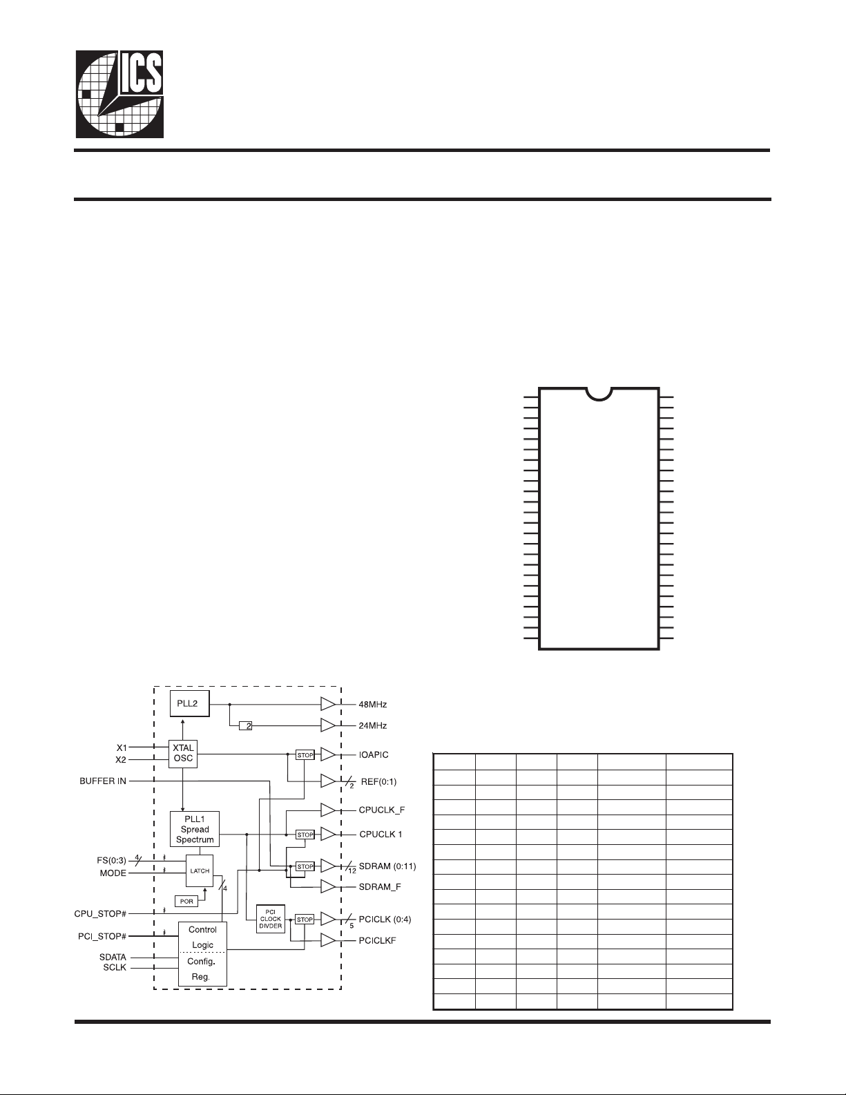
Pin Configuration
VDDREF
*SPREAD/REF0
GNDREF
*CPU2.5_3.3#/PCICLK_F
*SEL24_48#/PCICLK1
*SELPCIE_6#/PCICLK2
PCICLK6/
VDDPCI
*FS3/PCICLK0
GNDPCI
PCICLK3
PCICLK4
VDDPCI
BUFFER IN
GNDPCI
PCICLK5
PCICLK_E
VDDCOR
PCI_STOP#
*Vtt_PWRGD/PD#
GND48
SDATA
SCLK
1
2
3
X1
X2
4
5
6
7
8
9
10
11
12
13
14
15
16
17
18
19
20
21
22
23
24
48
47
46
45
44
43
42
41
40
39
38
37
36
35
34
33
ICS9248-195
32
31
30
29
28
27
26
25
TM
& K6
REF1/FS2*
VDDLCPU
CPUCLK_F
CPUCLK0
GNDLCPU
CPUCLK1
CPUCLK2
CLK_STOP#
GNDSDR
SDRAM_F
SDRAM0
SDRAM1
VDDSDR
SDRAM2
SDRAM3
GNDSDR
SDRAM4
SDRAM5
VDDSDR
SDRAM6
SDRAM7
VDD48
48MHz/FS0*
24_48MHz/FS1*
Block Diagram
0375D—02/02/04
48-Pin SSOP and TSSOP
* Internal Pull-up Resistor of 120K to VDD
Functionality
2tiB6tiB5tiB4tiBKLCUPCKLCICP
0000 76.6633.33
0001 00.00133.33
0010 76.6633.33
0011 33.33133.33
0100 76.6633.33
0101 00.00133.33
0110 00.00133.33
0111 33.33133.33
1000 76.6633.33
1001 00.00133.33
10 10 00.0900.03
10 11 33.33133.33
1100 00.0700.53
1101 00.50100.53
1110 33.33133.33
1111 00.04100.53
Page 2
ICS9248-195
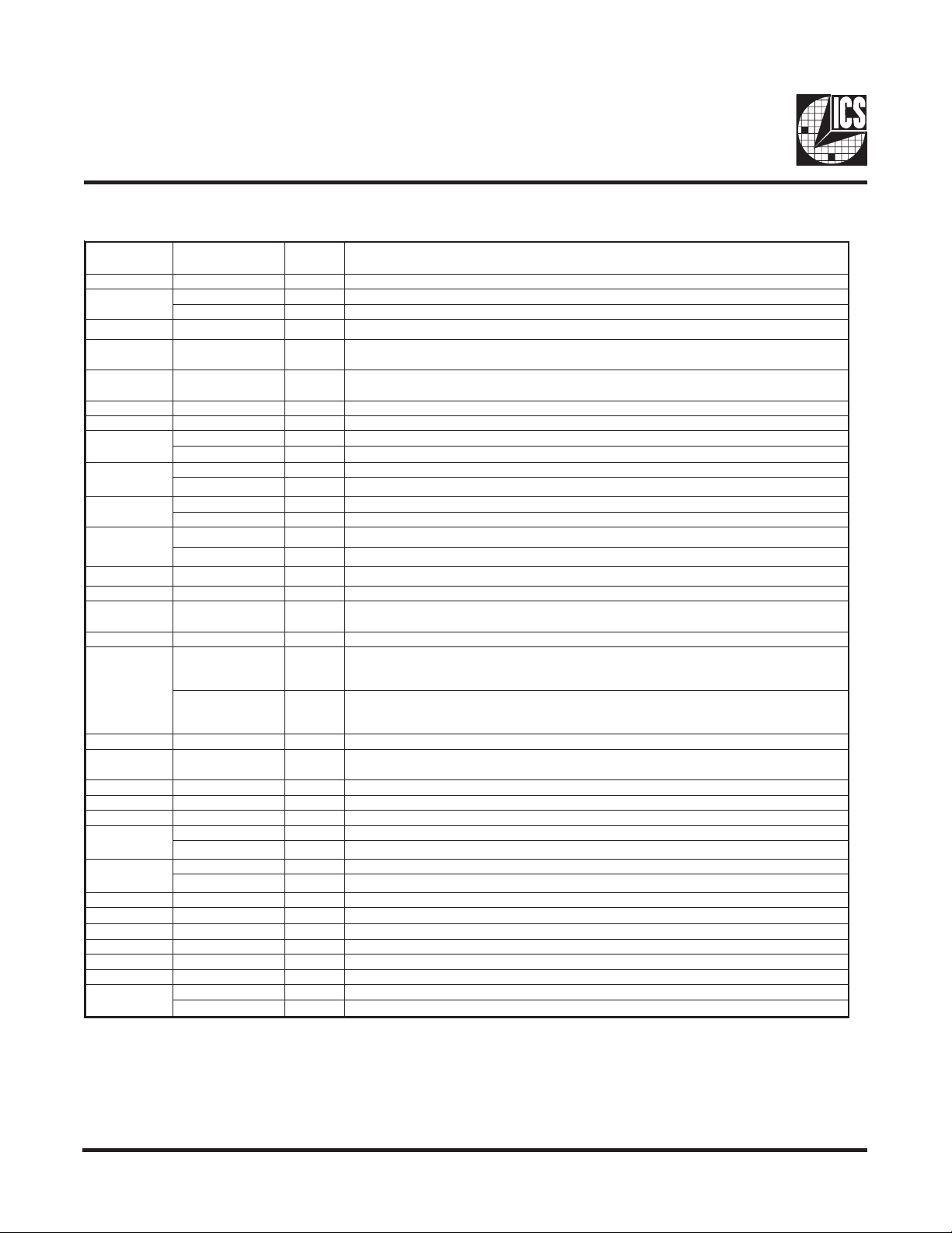
Pin Descriptions
NIP
REBMUN
1FERDDVRWPV3.3lanimon,ylppusrewopLATX,feR
2
0FERTUO sdaolSUBASIrofreffubREGNORTSehtsituptuoFERsihT.kcolcecnereferzhM813.41
02#POTS_ICPNI )0=EDOM,edomelibomnI(woltupninehw,level0cigoltaskcolcKLCICPstlaH
,61,9,3
DNGRWPdnuorG
44,04,33
41XNI
52XTUO.zHM813.41yllanimon,tuptuolatsyrC
41,6ICPDDVRWPV3.3lanimonKLCICPdnaF_KLCICProfylppuS
7
2,1
8
3SF
01
11
21,31,71)3:5(KLCICPTUO )ylraeUPC(wekssn4-1htiwskcolcUPCotsuonorhcnyS.stuptuokcolcICP
51NIREFFUBNI.stuptuoMARDSrofsreffuBtuonaFottupnI
81
E
91ROCDDVRWPV3.3.erocLLPehtrofniprewoP
12
1
#DP
2284DNGRWP.erocLLPdexif&sreffubtuptuozHM84&42ehtrofnipdnuorG
,23,13,92,82
83,73,53,43
63,03RDSDDVRWP.V3.3lanimon,eroCLLPUPCdnaMARDSrofylppuS
32ATADSNIIroftupniataD
42KLCSNIIfotupnikcolC
52
62
2,1
1SF
2,1
0SF
7284DDVRWP.erocLLPdexifdnasreffubtuptuozHM84&42rofrewoP
93F_MARDSTUO#POTS_UPCybdetceffatoN.tuptuokcolcMARDSgninnureerF
14#POTS_KLCNI .wolnevirdnehwlevel"0"cigoltaMARDS&,KLCUPCstlahtupnisuonorhcnysasihT
54,34,24)0:2(KLCUPCTUOUPCLDDVybderewop,stuptuokcolcUPC
64F_KLCUPCTUO#POTS_UPCehtybdetceffatoN.kcolcUPCgninnureerF
74UPCLDDVRWPV5.2skcolcUPCrofylppuS
84
1FERTUO.kcolcecnereferzHM813.41
2,1
2SF
Notes:
1: Internal Pull-up Resistor of 120K to 3.3V on indicated inputs
2: Bidirectional input/output pins, input logic levels are latched at internal power-on-reset. Use
10Kohm resistor to program logic Hi to VDD or GND for logic low.
EMANNIPEPYTNOITPIRCSED
2,1
DAERPS
NI "no"signidaerps,"hgiH"sitluafedpu-rewoP.tupnielbanemurtcepSdaerpShgiHevitcA
2Xmorfrotsiser
2,1
#3.3_5.2UPC
NI .tupnIdehctaL.UPCV3.3=WOL,UPCV5.2=hgiH.V3.3ro5.2siUPCLDDVrehtehwsetacidnI
F_KLCICPTUO .tnemeganamrewoprof#POTS_ICPybdetceffatonkcolcICPgninnureerF
NI.tupnIdehctaL.niptcelesycneuqerF
0KLCICPTUO )ylraeUPC(wekssn4-1htiwskcolcUPCotsuonorhcnyS.tuptuokcolcICP
2,1
#84_42LES
NIzHM84=woLnehwzHM84ro42rehtiestceleS
1KLCICPTUO )ylraeUPC(wekssn4-1htiwskcolcUPCotsuonorhcnyS.tuptuokcolcICP
2,1
#6_EICPLES
NI ).KLCICPylrae"hgiH"sitluafedpu-rewop81niprof(.tupnihctaltcelesICPlamronroylraEICP
2KLCICPTUO.tuptuokcolcKLCICP
-_KLCICP/6KLCICP
TUO #6_EICPLESybelbatcelestuptuokcolcICPylraerotuptuokcolcICP
DNGRWP_ttVNI
NI
)0:7(MARDSTUO .)tespihcybdellortnoc(nipNIREFFUBmorfstuptuoreffuBtuonaF,stuptuokcolcMARDS
2
2
zHM84_42TUO01nipybelbatceleskcolctuptuozHM84rozHM42
NI.tupnIdehctaL.niptcelesycneuqerF
zHM84TUOkcolctuptuozHM84
NItupnIdehctaL.niptcelesycneuqerF
NItupnIdehctaL.niptcelesycneuqerF
kcabdeefdna)Fp63(pacdaollanretnisah,tupnilatsyrC
.nipnwodrewopwolevitcasuonorhcnysa
.sm4nahtretaergebtonlliwnwodrewop
tupnitnarelotV5,tupnilairesC
tupnitnarelotV5,tupniC
nasinipehtretfaerehtnorewoptadehctaleblliwtcelesycneuqerfehthgihseog
DGRWP_ttVnehW.langis#DPdnaDGRWP_ttVrofniptupninoitcnuflaudasastcanipsihT
ehT.etatsrewopwolaotniecivedehtnwodrewopotdesuniptupniwolevitcasuonorhcnysA
ehtfoycnetalehT.deppotseralatsyrcehtdnaOCVehtdnadelbasideraskcolclanretni
0375D—02/02/04
2
Page 3
ICS9248-195
y
g
General Description
The ICS9248-195 is the single chip cloc k solution f or Notebook designs using the 440BX, MX, VIA PM/PL/PLE 133
style chip set, with Coppermine or T ualatin processor , for Note book applications. It pro vides all necessary clock signals
for such a system.
Spread spectrum may be enabled through I2C programming. Spread spectrum typically reduces system EMI by 8dB
to 10dB. This simplifies EMI qualification without resorting to board design iterations or costly shielding. The ICS9248-
195 employs a proprietary closed loop design, which tightly controls the percentage of spreading over process and
temperature variations.
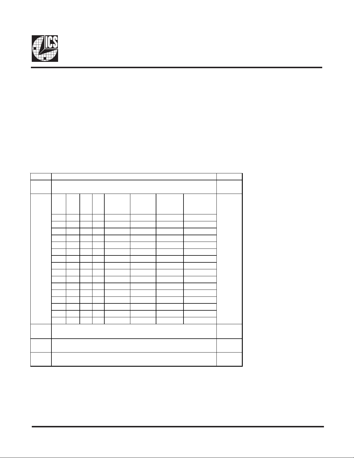
Serial Configuration Command Bitmap
Byte0: Functionality and Frequency Select Register (default = 0)
Bit PWD
0 = Center Spread Spec t rum M odul ation
Bit 7
1 = Down Spread S pec trum M odulation
FS3
FS2
FS1
FS0
Bit2
Bit6
Bit5
Bit4
0 0 0 0 66.67 33.33 ±0.35% -0.70%
0 0 0 1 100.00 33.33 ±0.35% -0.70%
0 0 1 0 66.67 33.33 ±0.60% -1.20%
0 0 1 1 133.33 33.33 ±0.35% -0.70%
0 1 0 0 66.67 33.33 ±0.23% -0.45%
Bit 2,
6:4
Bit 3
Bit 1
Bit 0
0 1 0 1 100.00 33.33 ±0.23% -0.45%
0 1 1 0 100.00 33.33 ±0.60% -1.20%
0 1 1 1 133.33 33.33 ±0.23% -0.45%
1 0 0 0 66.67 33.33 ±0.45% -0.90%
1 0 0 1 100.00 33.33 ±0.45% -0.90%
1 0 1 0 90.00 30.00 ±0.35% -0.70%
1 0 1 1 133.33 33.33 ±0.45% -0.90%
1 1 0 0 70.00 35.00 ±0.35% -0.70%
1 1 0 1 105.00 35.00 ±0.35% -0.70%
1 1 1 0 133.33 33.33 ±0.60% -1.20%
1 1 1 1 140.00 35.00 ±0.35% -0.70%
0 - Frequenc
1 - Frequency is c ontrolled by I
0 - Normal
1 - Spread Spec trum E nabl ed
0 - Runnin
1 - Tris t ate all out puts
is selected by hardware select pins. Lat ched input s.
Description
CPUCLK PCICLK
2
C programming.
Center
Spread %
Down
Spread%
Note1
0011
1
0
1
0
Notes:
1, Default at Power-up will be for latched logic inputs to define frequency. Bit [2, 6:4] are default to 0011.
2, PWD = Power-Up Default
0375D—02/02/04
3
Page 4
ICS9248-195
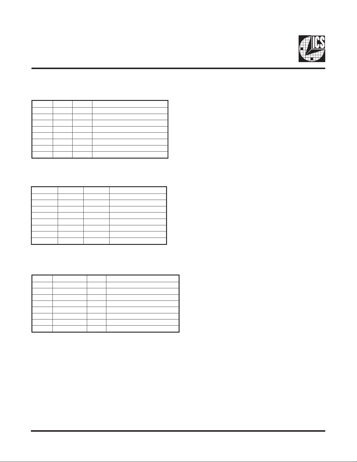
Byte 1: Active/Inactive Register (1 = enable, 0 = disable)
tiB#niPDWPnoitpircseD
7tiB-1 )devreseR(
6tiB641 )siD/nE(F_KLCUPC
5tiB-0 )devreseR(
4tiB-0 )devreseR(
3tiB931 )siD/nE(F_MARDS
2tiB241 )siD/nE(2KLCUPC
1tiB341 )siD/nE(1KLCUPC
0tiB541 )siD/nE(0KLCUPC
Byte 2: Active/Inactive Register (1 = enable, 0 = disable)
tiB#niPDWPnoitpircseD
7tiB71 )siD/nE(F_KLCICP
6tiB811 )siD/nE(6KLCICP
5tiB711 )siD/nE(5KLCICP
4tiB311 )siD/nE(4KLCICP
3tiB211 )siD/nE(3KLCICP
2tiB111 )siD/nE(2KLCICP
1tiB011 )siD/nE(1KLCICP
0tiB81 )siD/nE(0KLCICP
Byte 3: Active/Inactive Register (1 = enable, 0 = disable)
tiB#niPDWPnoitpircseD
7tiB-1 )devreseR(
6tiB-0 )devreseR(
5tiB-0 )devreseR(
4tiB-0 )devreseR(
3tiB821 )siD/nE(7MARDS
2tiB921 )siD/nE(6MARDS
1tiB131 )siD/nE(5MARDS
0tiB231 )siD/nE(4MARDS
Notes:
1. Inactive means outputs are held LOW and are disabled from switching.
2. Latched register v alues will be inv erted from pin values. Def ault latch condition is for all latched inputs to
be floating (pulled up via internal resistor) at power-up.
0375D—02/02/04
4
Page 5
Byte 4: Active/Inactive Register (1 = enable, 0 = disable)
tiB#niPDWPnoitpircseD
7tiB-1 )devreseR(
6tiB-0 )devreseR(
5tiB-0 #)84_42LES(
4tiB-0 #0SFdehctaL
3tiB-0 #1SFdehctaL
2tiB-0 #2SFdehctaL
1tiB-0 #3SFdehctaL
0tiB-1 )devreseR(
Byte 5: Active/Inactive Register (1 = enable, 0 = disable)
tiB#niPDWPnoitpircseD
7tiB431 )siD/nE(3MARDS
6tiB531 )siD/nE(2MARDS
5tiB731 )siD/nE(1MARDS
4tiB831 )siD/nE(0MARDS
3tiB621 )siD/nE(zHM84
2tiB521 )siD/nE(zHM42
1tiB841 )siD/nE(1FER
0tiB21 )siD/nE(0FER
ICS9248-195
Notes:
1. Inactive means outputs are held LOW and are disabled from switching.
2. Latched register v alues will be inverted from pin values. Default latch condition is for all latched inputs to be floating
(pulled up via internal resistor) at power-up.
0375D—02/02/04
5
Page 6

ICS9248-195
D
D
t
Absolute Maximum Ratings
Supply Voltage . . . . . . . . . . . . . . . . . . . . . . . 5.5 V
Logic Inputs . . . . . . . . . . . . . . . . . . . . . . . . . GND –0.5 V to VDD +0.5 V
Ambient Operating Temperature . . . . . . . . . . 0°C to +70°C
Case Temperature . . . . . . . . . . . . . . . . . . . . . 115°C
Storage Temperature. . . . . . . . . . . . . . . . . . . –65°C to +150°C
Stresses above those listed under
ratings are stress specifications only and functional operation of the device at these or any other conditions above those
listed in the operational sections of the specifications is not implied. Exposure to absolute maximum rating conditions
for extended periods ma y aff ect product reliability.
Electri cal Character i st ics - I nput/ Supply/Common O utput Param eter s
TA = 0 - 70°C; Sup pl y V ol tage VDD = V
PARAMETER SYMBOL CONDITIONS MIN TYP MAX UNITS
Input High Voltage V
Input Low V ol tage V
Operat i ng Supply
Current
Powerd own C urren t
Input Freque ncy F
Input Capac i tanc e
Clk Stabilization
Skew
1
Guarant eed by design, not 10 0% test ed i n product ion.
1
1
1
IH
IL
I
DD3.3OP
I
DDPD
i
C
IN
C
INX
T
STAB
t
CPU-PCI1VT
Absolute Maximum Ratings
= 3.3 V +/ -5% (unless ot herwi se s tated)
DDL
= 0 pF ; Se l ect @ 66MHz 150
C
L
C
= 0 pF ; Se l ect @ 100 M Hz 170
L
= 0 pF ; Se l ect @ 133 M Hz 180
C
L
CL = 0 pF ; I nput address V DD or GND 600
V
= 3.3 V 14.32 MHz
D
may cause permanent damage to the device. These
2V
V
- 0. 3 0. 8 V
SS
+ 0.3 V
DD
mA
µA
Logic Inputs 5 pF
X1 & X2 pins 27 45 pF
From VDD = 3.3 V to 1% target Freq. 5.5 ms
= 1.5 V
14ns
Elect r i ca l Charac t er i st ics - Input / Suppl y/ Com m on O ut put Par ame t er s
TA = 0 - 70°C; Supp l y Vo l tage VDD = 3.3 V +/-5%, V
PARAMETER SYMBOL CONDITIONS MIN TYP MA X UNITS
= 0 pF ; S el ect @ 66 . 8 M Hz 15
C
L
perating SupplyCurren
Powerdown Current
1
Skew
1
Guarant eed by design, not 10 0% test ed i n product i o n.
0375D—02/02/04
I
DDL2.5
I
DDLP
t
CPU-PCI2
C
= 0 pF ; S el ect @ 10 0 M Hz 18
L
= 0 pF ; S el ect @ 13 3 M Hz 25
C
L
CL = 0 pF; Input addres s V DD or GND
VT = 1.5 V ; VTL = 1.25 V
= 2.5 V +/ -5% (unless otherwise st ated)
DDL
14ns
6
10
mA
mA
Page 7

ICS9248-195
Electrical Characterist i cs - CPU
TA = 0 - 70°C; VDD = 3. 3 V +/ -5% ; CL = 20 pF
PARAMETER SYMBOL CONDITIONS MIN TYP MAX UNITS
Output High Volt age V
Output Low V oltage V
Out put Hi gh Cu rrent I
Output Low Current I
Rise Time
Fall Time
Duty Cycle
Skew wi ndo w
1
1
1
1
Jitter, Cycle-to-cycle
1
Guaranteed by design, not 100% t es ted in produc t i on.
OH2AIOH
OL2A
OH2A
OL2A
t
r2A
t
f2A
d
t2A
t
sk2A
1
t
jcyc-cyc2AVT
= -20 mA 2.4 V
IOL = 12 mA 0.4 V
VOH = 2. 0 V -27 mA
VOL = 0. 8 V 22 m A
VOL = 0. 4 V , VOH = 2. 4 V 1.35 2 ns
VOH = 2.4 V, VOL = 0. 4 V 1.44 2 ns
VT = 1. 5 V 45 50. 3 55 %
VT = 1. 5 V 70 175 ps
= 1.5 V
160 250 ps
Electrical Characteristics - CPU
TA = 0 - 70°C; V
PARAME TER SYMBOL CONDITIONS MIN TYP MAX UNITS
Output High Volt age V
Output Low V ol t age V
Output High Current I
Out put Low Curre nt I
Rise T im e
Fall Time
Duty Cycle
Sk ew window
Jitter, Cycle-to-cycle
1
Guaranteed by des i gn, not 100% tes ted in produc t i on.
= 2. 5 V +/ -5% ; CL = 20 pF
DDL
OH2B
OL2B
OH2B
1
1
1
1
OL2B
t
t
t
sk2B
1
t
jcyc-cyc2BVT
r2B
f2B
t2B
IOH = -12 mA 2 V
IOL = 12 mA 0.4 V
VOH = 1. 7 V -21 mA
VOL = 0. 7 V 22 mA
VOL = 0. 4 V , VOH = 2.0 V 1.40 1.8 ns
VOH = 2.0 V, VOL = 0.4 V 1.70 1.8 ns
V
V
VT = 1. 25 V 60 175 ps
= 1. 25 V , < 133 M Hz 45 52 55
T
= 1. 25 V , > = 133 M Hz 42 51 52
T
= 1. 25 V
143 250 ps
%d
0375D—02/02/04
7
Page 8

ICS9248-195
y Cy
Electrical Characteri st i cs - PCI
TA = 0 - 70°C; VDD = 3.3 V +/-5%; CL = 30 pF
PARAMETER SYMBOL CONDITIONS MIN TYP MAX UNITS
Output High V ol t age V
Output Low Vol t age V
Output High Current I
Output Low Current I
Rise T i me
Fall Time
Duty Cycle
Sk ew window
Sk ew window
Jitter, Absolute
1
Guaranteed by des i gn, not 100% tes t ed in produc t i on.
1
1
1
1
1
1
OH1
OL1
t
t
d
t
sk1
t
sk2
t
jabs1
OH1
OL1
r1
f1
IOH = -1 8 m A 2.4 V
IOL = 9. 4 m A 0.4 V
VOH = 2. 0 V -33 mA
VOL = 0.8 V 38 mA
VOL = 0.4 V, VOH = 2. 4 V 1.60 2.2 ns
VOH = 2.4 V, VOL = 0. 4 V 1.50 2.2 ns
VT = 1. 5 V 45 51. 5 55 %
t1
VT = 1. 5 V 380 500 ps
VT = 1.5 V PCICLKE to PCI [5:0] 2 2.71 4 ns
VT = 1. 5 V
120 250 ps
El e c tri c a l Chara c terist ics - SDRAM
TA = 0 - 70°C; VDD = 3.3 V +/-5%; CL = 30 pF
PARAMETER SYMBOL CONDITIONS MIN TYP MAX UNITS
Output High V ol t age V
Output Low Vol t age V
Output High Current I
Output Low Current I
cle
1
1
1
1
1
Rise T i me
Fall Time
Dut
Sk ew window
Propagati on Ti m e
(Buffer In to output)
1
Guaranteed by des i gn, not 100% tes t ed in produc tion.
OH3
T
T
D
T
T
OH3
OL3
OL3
sk3
sk3
IOH = -2 8 m A 2.4 V
IOL = 19 mA 0.4 V
VOH = 2. 0 V -46 mA
VOL = 0.8 V 32 mA
VOL = 0.4 V, VOH = 2. 4 V 1.17 1.6 ns
r3
VOH = 2.4 V, VOL = 0. 4 V 1.20 1.6 ns
f3
VT = 1. 5 V 42 50 52 %
t3
VT = 1. 5 V 210 250 ps
VT = 1. 5 V 4.10 5 ns
0375D—02/02/04
8
Page 9

ICS9248-195
Electrical Characteri st i cs - 24, 48M Hz
TA = 0 - 70°C; VDD = 3.3 V +/-5%; CL = 10 - 20 pF (unles s otherwis e s t ated)
PARAMETER SYMBOL CONDITIONS MIN TYP MAX UNITS
Output High V ol t age V
Output Low Vol t age V
Output High Current I
Output Low Current I
Rise T i m e
Fall Time
Duty Cycle
Jitter, Absolute
1
Guaranteed by des i gn, not 100% t es t ed i n production.
1
1
1
1
OH5
OL5
OH5
OL5
t
t
d
t
CYCLE
r5
f5
IOH = -1 4 m A 2.4 V
IOL = 6 mA 0.4 V
VOH = 2. 0 V -20 mA
VOL = 0.8 V 16 mA
VOL = 0.4 V, VOH = 2. 4 V 1.93 4 ns
VOH = 2.4 V, VOL = 0. 4 V 2.63 4 ns
VT = 1. 5 V 45 50.9 55 %
t5
VT = 1. 5 V
436 600 ps
Electrical Characteri st i cs - REF
TA = 0 - 70°C; VDD = 3. 3 V + / -5% ; CL = 10 - 20 pF (unl ess otherwise s tat ed)
PARAMETER SYMBOL CONDITIONS MIN TYP MAX UNITS
Output High Volt age V
Output Low Voltage V
Output Hi gh Current I
Output Low Current I
Rise T i m e
Fall Time
Duty Cycl e
Jitter, cycle to cycle
1
Guaranteed by des i gn, not 100% t est ed i n product i on.
1
1
1
1
OH5
OL5
OH5
OL5
t
t
d
t
jcycle5
IOH = -14 mA 2.4 2.6 V
IOL = 6 mA 0.22 0.4 V
VOH = 2.0 V -32 -20 mA
VOL = 0. 8 V 16 22 mA
VOL = 0. 4 V , VOH = 2.4 V 2.11 4 ns
r5
VOH = 2.4 V , VOL = 0.4 V 2.14 4 ns
f5
VT = 1. 5 V 45 52.1 55 %
t5
VT = 1. 5 V
-600 848 1000 ps
0375D—02/02/04
9
Page 10

ICS9248-195
K
0
2
3
5
K
K
K
K
K
K
K
K
The information in this section assumes familiarity with I2C programming.
For more information, contact ICS for an I2C programming application note.
General I2C serial interface information
How to Write:
• Controller (host) sends a start bit.
• Controller (host) sends the write address D2
• ICS clock will acknowledge
• Controller (host) sends a dummy command code
• ICS clock will acknowledge
• Controller (host) sends a dummy byte count
• ICS clock will acknowledge
• Controller (host) starts sending first byte (Byte 0)
through byte 5
• ICS clock will acknowledge each byte one at a time.
• Controller (host) sends a Stop bit
How to Write:
Controller (Host) ICS (Slave/Receiver)
Start Bit
Address
D2
(H)
Dummy Command Code
Dummy Byte Count
Byte 0
Byte 1
Byte 2
Byte 3
Byte 4
Byte 5
Stop Bit
(H)
AC
AC
AC
AC
AC
ACK
AC
AC
AC
How to Read:
• Controller (host) will send start bit.
• Controller (host) sends the read address D3
• ICS clock will acknowledge
• ICS clock will send the byte count
• Controller (host) acknowledges
• ICS clock sends first byte (Byte 0) through byte 5
• Controller (host) will need to acknowledge each byte
• Controller (host) will send a stop bit
How to Read:
Controller (Host) ICS (Slave/Receiver)
Start Bit
Address
D3
(H)
ACK
ACK
ACK
ACK
ACK
ACK
ACK
Stop Bit
AC
Byte Count
Byte
Byte 1
Byte
Byte
Byte 4
Byte
(H)
Notes:
1. The ICS clock generator is a slav e/receiver , I2C component. It can read bac k the data stored in the latches for
verification. Read-Back will support Intel PII/PIII "Block-Read" protocol.
2. The data transfer rate supported by this clock generator is 100K bits/sec or less (standard mode)
3. The input is operating at 3.3V logic levels.
4. The data byte format is 8 bit bytes.
5. T o simplify the clock generator I2C interface, the protocol is set to use only "Block-Writes" from the controller .
The bytes must be accessed in sequential order from lowest to highest byte with the ability to stop after any
complete byte has been transferred. The Command code and Byte count shown abo ve must be sent, but the
data is ignored for those two b ytes . The data is loaded until a Stop sequence is issued.
6. At power-on, all registers are set to a default condition, as shown.
0375D—02/02/04
10
Page 11

Shared Pin Operation Input/Output Pins
ICS9248-195
The I/O pins designated by (input/output) serve as dual
signal functions to the device. During initial power-up,
they act as input pins. The logic level (voltage) that is
present on these pins at this time is read and stored into
a 5-bit internal data latch. At the end of P ower-On reset,
(see AC characteristics for timing values), the device
changes the mode of operations for these pins to an
output function. In this mode the pins produce the
specified buffered clocks to external loads.
To program (load) the internal configuration register for
these pins, a resistor is connected to either the VDD
(logic 1) power supply or the GND (logic 0) voltage
potential. A 10 Kilohm (10K) resistor is used to provide
both the solid CMOS programming voltage needed during
the power-up programming period and to provide an
insignificant load on the output clock during the subsequent
operating period.
Figure 1 shows a means of implementing this function
when a switch or 2 pin header is used. With no jumper is
installed the pin will be pulled high. With the jumper in
place the pin will be pulled low . If progr ammability is not
necessary , than only a single resistor is necessary. The
programming resistors should be located close to the
series termination resistor to minimize the current loop
area. It is more important to locate the series termination
resistor close to the driver than the programming resistor .
0375D—02/02/04
Programming
Header
Via to Gnd
Device
Pad
Via to
VDD
2K W
8.2K W
Clock trace to load
Series Term. Res.
Fig. 1
11
Page 12

ICS9248-195
PD# Timing Diagram
The power down selection is used to put the part into a very low power state without turning off the power to the part.
PD# is an asynchronous active low input. This signal needs to be synchronized internal to the device prior to powering
down the clock synthesizer .
Internal clocks are not running after the device is put in power down. When PD# is active lo w all clocks need to be driven
to a low value and held prior to turning off the VCOs and crystal. The pow er up latency needs to be less than 4 mS.
The power down latency should be as short as possible but conf orming to the sequence requirements shown below.
PCI_STOP# and CLK_ST OP# are considered to be don't cares during the power down operations. The REF and 48MHz
clocks are expected to be stopped in the LOW state as soon as possible. Due to the state of the internal logic, stopping
and holding the REF clock outputs in the LOW state may require more than one clock cycle to complete.
PD#
CPUCLK
PCICLK
VCO
Crystal
Notes:
1. All timing is referenced to the Internal CPUCLK (defined as inside the ICS9248 device).
2. As shown, the outputs Stop Low on the next falling edge after PD# goes low.
3. PD# is an asynchronous input and metastable conditions may exist. This signal is synchronized inside this part.
4. The shaded sections on the VCO and the Crystal signals indicate an active clock.
5. Diagrams shown with respect to 133MHz. Similar operation when CPU is 100MHz.
0375D—02/02/04
12
Page 13

ICS9248-195
CLK_STOP# Timing Diagram
CLK_STOP# is an asychronous input to the clock synthesize r. It is used to turn off the CPU clocks for low power
operation. CLK_STOP# is synchronized by the ICS9248-195. The minimum that the CPU clock is enabled (CLK_ST OP#
high pulse) is 100 CPU clocks. All other clocks will continue to run while the CPU clocks are disabled. The CPU clocks
will always be stopped in a lo w state and start in such a manner that guarantees the high pulse width is a full pulse.
CPU clock on latency is less than 4 CPU clocks and CPU clock off latency is less than 4 CPU clocks.
INTERNAL
CPUCLK
PCICLK
CLK_STOP#
PCI_STOP# (High)
SDRAM
CPUCLK
CPUCLK _F
SDRAM_F
Notes:
1. All timing is referenced to the internal CPU clock.
2. CLK_STOP# is an asynchronous input and metastable conditions may exist. This signal is
synchronized to the CPU clocks inside the ICS9248-195.
3. SDRAM-F output is controlled by Buffer in signal, not affected by the ICS9248-195
CLK_STOP# signal. SDRAM are controlled as shown.
4. All other clocks continue to run undisturbed.
0375D—02/02/04
13
Page 14

ICS9248-195
PCI_STOP# Timing Diagram
PCI_STOP# is an asynchronous input to the ICS9248-195. It is used to turn off the PCICLK clocks for low power
operation. PCI_STOP# is synchronized by the ICS9248-195 internally. The minimum that the PCICLK clocks are
enabled (PCI_ST OP# high pulse) is at least 10 PCICLK clocks. PCICLK cloc ks are stopped in a low state and started
with a full high pulse width guaranteed. PCICLK clock on latency cycles are only three rising PCICLK clocks, off latency
is one PCICLK clock.
CPUCLK
(Internal)
PCICLK_F
(Internal)
PCICLK_F
(Free-running)
CLK_STOP#
PCI_STOP#
PCICLK
Notes:
1. All timing is referenced to the Internal CPUCLK (defined as inside the ICS9248 device.)
2. PCI_STOP# is an asynchronous input, and metastable conditions may exist. This signal is required to be synchronized
inside the ICS9248.
3. All other clocks continue to run undisturbed.
4. CLK_STOP# is shown in a high (true) state.
0375D—02/02/04
14
Page 15

ICS9248-195
INDEX
AREA
1 2
h x 45°
SEATING
PLANE
- C -
.10 (.004) C
α
N
INDEX
AREA
12
D
e
b
300 mil SSOP Package
c
SYMBOL
L
E1
E
A 2.41 2.80 .095 .110
A1 0.20 0.40 .008 .016
b 0.20 0.34 .008 .0135
In Millimeters In Inches
COMMON DIMENSIONS COMMON DIMENSIONS
MIN MAX MIN MAX
c 0.13 0.25 .005 .010
D
SEE VARIATIONS SEE VARIATIONS
E 10.03 10.68 .395 .420
E1 7.40 7.60 .291 .299
h x 45°
α
e
0.635 BASIC 0.025 BASIC
h 0.38 0.64 .015 .025
L 0.50 1.02 .020 .040
N
A
A1
-C-
SEATING
PLANE
.10 (.004) C
N
48 15.75 16.00 .620 .630
Reference Doc.: JEDEC Publication 95, MO-118
10-0034
SEE VARIATIONS SEE VARIATIONS
0° 8° 0° 8°
VARIATIONS
D mm. D (inch)
MIN MAX MIN MAX
Ordering Information
ICS9248yF-195LF-T
Example:
ICS XXXX y F LF- T
0375D—02/02/04
Designation for tape and reel packaging
Lead Free (Optional)
Package Type
F = SSOP
Revision Designator (will not correlate with datasheet revision)
Device T ype
Prefix
ICS = Standard Device
15
Page 16

ICS9248-195
INDEX
AREA
1 2
SEATING
PLANE
- C -
N
E1
INDEX
AREA
12
D
A2
e
b
E
A
A1
aaa
(240 mil)
(0.020 mil)
6.10 mm. Body , 0.50 mm. pitch TSSOP
c
-C-
SEATING
PLANE
C
In Millimeters In Inches
SYMBOL
L
COMMON DIMENS IONS CO M MON DIM ENSIO NS
MIN MAX MIN MAX
A -- 1.20 -- .047
A1 0.05 0.15 .002 .006
A2 0.80 1.05 .032 .041
b 0.17 0.27 .007 .011
c 0.09 0.20 .0035 .008
D
E
E1 6.00 6.20 .236 .244
e
SEE VARIATIONS SEE VARIATIONS
8.10 BA S IC 0.319 BASIC
0.50 BA S IC 0.020 BASIC
L 0.45 0.75 .018 .030
N
α
SEE VARIATIONS SEE VARIATIONS
0° 8° 0° 8°
aaa -- 0.10 -- .004
VARIATIONS
N
D mm . D (inch)
MIN MAX MIN MAX
48 12.40 12.60 .488 .496
Ref er ence Do c.: JEDEC Pub lication 95, M O-153
10-0039
0375D—02/02/04
Ordering Information
ICS9248yG-195LF-T
Example:
ICS XXXX y G LF- T
Designation for tape and reel packaging
Lead Free (Optional)
Package Type
G = TSSOP
Revision Designator (will not correlate with datasheet revision)
Device T ype
Prefix
ICS = Standard Device
16
 Loading...