

Page 1

查询ICS85356AGI供应商
Integrated
Circuit
Systems, Inc.
GENERAL DESCRIPTION
ICS
HiPerClockS™
the CLKxx input pairs will be passed to the output. When
COM_SEL is logic Low, the output is determined by the setting
of the SEL0 pin for channel 0 and the SEL1 pin for Channel 1.
The differential input has a common mode range that can accept
most differential input types such as LVPECL, LVDS, LVHSTL,
SSTL, and HCSL. The ICS85356I can therefore be used as a
differential translator to translate almost any differential input type
to LVPECL. It can also be used in ECL mode by setting V
and V
The ICS85356I adds negligible jitter to the input clock and can
operate at high frequencies in excess of 900MHz thus making
it ideal for use in demanding applications such as SONET,
Fibre Channel, 1 Gigabit/10 Gigabit Ethernet.
The ICS85356I is a dual 2:1 Differential-to-LVPECL
Multiplexer and is a member of the HiPerClockS
family of High Performance Clock Solutions from
ICS. The device has both common select and individual select inputs. When COM_SEL is logic High,
to -3.0V to - 3.8V.
EE
CC
TM
=0V
ICS85356I
2:1, DIFFERENTIAL-TO-3.3V
DUAL LVPECL / ECL CLOCK MULTIPLEXER
FEATURES
• High speed differential multiplexer.
The device can be configured as a 2:1 multiplexer
• Dual 3.3V LVPECL outputs
• Selectable differential CLKxx, nCLKxx inputs
• CLKxx, nCLKxx pair can accept the following differential
input levels: LVPECL, LVDS, LVHSTL, SSTL, HCSL
• Output frequency: 900MHz (typical)
• Translates any single ended input signal to 3.3V
LVPECL levels with resistor bias on nCLKxx input
• Output skew: 75ps (typical)
• Propagation delay: 1.15ns (typical)
• LVPECL mode operating voltage supply range:
= 3V to 3.8V, VEE = 0V
V
CC
• ECL mode operating voltage supply range:
= 0V, VEE = -3V to -3.8V
V
CC
• -40°C to 85°C ambient operating temperature
• Lead-Free package available
• Compatible with MC100LVEL56
BLOCK DIAGRAM PIN ASSIGNMENT
CLK0A
nCLK0A
CLK0B
nCLK0B
SEL0
COM_SEL
SEL1
CLK0A
0
1
Q0
nQ0
nCLK0A
CLK0B
nCLK0B
CLK1A
nCLK1A
CLK1B
nCLK1B
nc
nc
1
2
3
4
5
6
7
8
9
10
20
19
18
17
16
15
14
13
12
11
V
CC
Q0
nQ0
SEL0
COM_SEL
SEL1
V
CC
Q1
nQ1
V
EE
CLK0A
nCLK0A
CLK0B
nCLK0B
CLK1A
nCLK1A
CLK1B
nCLK1B
ICS85356I
CLK1A
nCLK1A
CLK1B
nCLK1B
85356AMI www.icst.com/products/hiperclocks.html REV. A OCTOBER 7, 2004
0
1
Q1
nQ1
1
20-Lead SOIC
7.5mm x 12.8mm x 2.3mm
M Package
Top View
6.5mm x 4.4mm x 0.92mm
1
2
nc
3
4
5
6
7
nc
8
9
10
ICS85356I
20-Lead TSSOP
G Package
Top View
20
19
18
17
16
15
14
13
12
11
V
CC
Q0
nQ0
SEL0
COM_SEL
SEL1
V
CC
Q1
nQ1
V
EE
Page 2
Integrated
Circuit
Systems, Inc.
2:1, DIFFERENTIAL-TO-3.3V
DUAL LVPECL / ECL CLOCK MULTIPLEXER
TABLE 1. PIN DESCRIPTIONS
rebmuNemaNepyTnoitpircseD
02,41V
1A0KLCtupnInwodlluP.tupnikcolclaitnereffidgnitrevni-noN
2A0KLCntupnIpulluP.tupnikcolclaitner
8,3cndesunU.tcennocoN
4B0KLCtupnInwodlluP.tupnikcolclaitnereffidgnitrevni-noN
5B0KLCntupnIpulluP.tup
6A1KLCtupnInwodlluP.tupnikcolclaitnereffidgnitrevni-noN
7A1KLCntupnIpulluP.tupnikc
9B1KLCtupnInwodlluP.tupnikcolclaitnereffidgnitrevni-noN
01B1KLCntupnIpulluP.tupnikcolc
11V
31,211Q,1QntuptuO.slevelecafretniLCEPVL.sriaptuptuolaitnereffiD
511LEStupnIpulluP.slev
61LES_MOCtupnInwodlluP.slevelecafretniLTTVL/SOMCVL.tupnitcelesnom
710LEStupnIpulluP.slevelecafretniLTTVL/SOMCVL.tupnitceleskcolC
91,810Q,0QntuptuO.slevelecafretniLCEPVL.sri
:ETON
pulluP
CC
EE
dna
nwodlluP
rewoP.nipylppuseroC
effidgnitrevnI
nikcolclaitnereffidgnitrevnI
olclaitnereffidgnitrevnI
laitnereffidgnitrevnI
rewoP.snipylppusevitageN
moC
aptuptuolaitnereffiD
ICS85356I
elecafretniLTTVL/SOMCVL.tupnitceleskcolC
.seulavlacipytrof,scitsiretcarahCniP,2elbaTeeS.srotsisertupnilanretniotrefer
TABLE 2. PIN CHARACTERISTICS
lobmySretemaraPsnoitidnoCtseTmuminiMlacipyTmumixaMstinU
C
NI
R
PULLUP
R
NWODLLUP
ecnaticapaCtupnI 4Fp
rotsiseRpulluPtupnI 15KΩ
rotsiseRnwodlluPtupnI 15KΩ
TABLE 3. CONTROL INPUT FUNCTION TABLE
stupnIstuptuO
LES_MOC1LES0LES0Q0Qn1Q1Qn
000 A0KLCA0KLCnA1KLCA1KLCn
00 1 B0KLCB0KLCnA1KLCA1KLCn
010 A0KLCA0KLCnB1KLCB1KLCn
011 B0KLCB0KLCnB1KLCB1KLCn
1XX B0KLCB0KLCnB1KLCB1KLCn
85356AMI www.icst.com/products/hiperclocks.html REV. A OCTOBER 7, 2004
2
Page 3
Integrated
Circuit
Systems, Inc.
ABSOLUTE MAXIMUM RATINGS
ICS85356I
2:1, DIFFERENTIAL-TO-3.3V
DUAL LVPECL / ECL CLOCK MULTIPLEXER
Supply Voltage, V
Inputs, V
I
Outputs, I
Continuous Current 50mA
CC
O
4.6V
-0.5V to V
+ 0.5V
CC
Surge Current 100mA
Package Thermal Impedance, θ
Storage Temperature, T
STG
TABLE 4A. POWER SUPPLY DC CHARACTERISTICS, V
46.2°C/W (0 lfpm)
JA
-65°C to 150°C
= 3.3V±0.3V, TA = -40°C TO 85°C
CC
lobmySretemaraPsnoitidnoCtseTmuminiMlacipyTmumixaMstinU
V
CC
I
EE
egatloVylppuSevitisoP 0.33.36.3V
tnerruCylppuSrewoP 04Am
TABLE 4B. LVCMOS / LVTTL DC CHARACTERISTICS, V
lobmySretemaraPsnoitidnoCtseTmuminiMlacipyTmumixaMstinU
V
HI
V
LI
I
HI
I
LI
egatloVhgiHtupnILES_MOC,1LES,0LES2V
egatloVwoLtupnILES_MOC,1LES,0LES3.0-8.0V
tnerruChgiHtupnI
tnerruCwoLtupnI
1LES,0LESV
LES_MOCV
1LES,0LESV
LES_MOCV
NOTE: Stresses beyond those listed under Absolute
Maximum Ratings may cause permanent damage to the
device. These ratings are stress specifications only. Functional
operation of product at these conditions or any conditions beyond those listed in the
istics
is not implied. Exposure to absolute maximum rating
conditions for extended periods may affect product reliability.
= 3.3V±0.3V, TA = -40°C TO 85°C
CC
V=
CC
V=
CC
CC
CC
V6.3=5Aµ
NI
V6.3=051Aµ
NI
V,V6.3=
V0=051-Aµ
NI
V,V6.3=
V0=5-Aµ
NI
DC Characteristics
or
AC Character-
3.0+V
CC
TABLE 4C. DIFFERENTIAL DC CHARACTERISTICS, V
= 3.3V±0.3V, TA = -40°C TO 85°C
CC
lobmySretemaraPsnoitidnoCtseTmuminiMlacipyTmumixaMstinU
,B0KLC,A0KLC
I
HI
tnerruChgiHtupnI
B1KLC,A1KLC
,B0KLCn,A0KLCn
B1KLCn,A1KLCn
,B0KLC,A0KLC
I
LI
tnerruCwoLtupnI
B1KLC,A1KLC
B1KLCn,A1KLCn
V
PP
V
RMC
85356AMI www.icst.com/products/hiperclocks.html REV. A OCTOBER 7, 2004
egatloVkaeP-ot-kaeP 51.00.1V
V
,B0KLCn,A0KLCn
V
2,1ETON;egatloVtupnIedoMnommoCV
.
VsadenifedsiegatlovtupniedomnommoC:1ETON
HI
V=
V
CC
V=
V
CC
CC
CC
3
V6.3=051Aµ
NI
V6.3=5Aµ
NI
V,V6.3=
V0=5-Aµ
NI
V,V6.3=
V0=051-Aµ
NI
5.0+V
EE
VsixKLCn,xKLCrofegatlovtupnimumixameht,snoitacilppadedneelgnisroF:2ETON
.V3.0+
58.0-V
CC
Page 4
Integrated
Circuit
Systems, Inc.
ICS85356I
2:1, DIFFERENTIAL-TO-3.3V
DUAL LVPECL / ECL CLOCK MULTIPLEXER
TABLE 4D. LVPECL DC CHARACTERISTICS, V
= 3.3V±0.3V, TA = -40°C TO 85°C
CC
lobmySretemaraPsnoitidnoCtseTmuminiMlacipyTmumixaMstinU
V
HO
V
LO
V
GNIWS
TABLE 5. AC CHARACTERISTICS, V
1ETON;egatloVhgiHtuptuOV
1ETON;egatloVwoLtuptuOV
gniwSegatloVtuptuOkaeP-ot-kaePIJ zHM0076.00.1V
05htiwdetanimretstuptuO:1ETON Ω Vot
= 3.3V±0.3V, TA = -40°C TO 85°C
CC
.V2-
CC
4.1-V
CC
0.2-V
CC
lobmySretemaraPsnoitidnoCtseTmuminiMlacipyTmumixaMstinU
f
XAM
t
DP
t
)o(ks3,2ETON;wekStuptuO 57051sp
t
R
t
F
t
cdo
ycneuqerFtuptuO 009zHM
1ETON;yaleDnoitagaporPIJ zHM00958.051.154.1sn
emiTesiRtuptuO%08ot%02002085sp
emiTllaFtuptuO%08ot%02002085sp
wekSelcyCytuD 001sp
ƒtaderusaemsretemarapllA ≤ zHM226.esiwrehtodetonsselnu
hT
.rettijelbarusaemddatonseodtrapsi
.tniopgnissorctuptuolaitnereffidehtottniopgnissorctupnilaitnereffidehtmorfderusaeM:1ETON
daollauqehtiwdnaegatlovylppusemasehttastuptuoneewtebwekssadenifeD:2ETON
ehttaderusaeM
.stniopssorclaitnereffidtuptuo
.snoitidnoc
.56dradnatSCEDEJhtiwecnadroccanidenifedsiretemarapsihT:3ETON
0.1-V
CC
7.1-V
CC
85356AMI www.icst.com/products/hiperclocks.html REV. A OCTOBER 7, 2004
4
Page 5
2V
V
CC
LVPECL
V
EE
Integrated
Circuit
Systems, Inc.
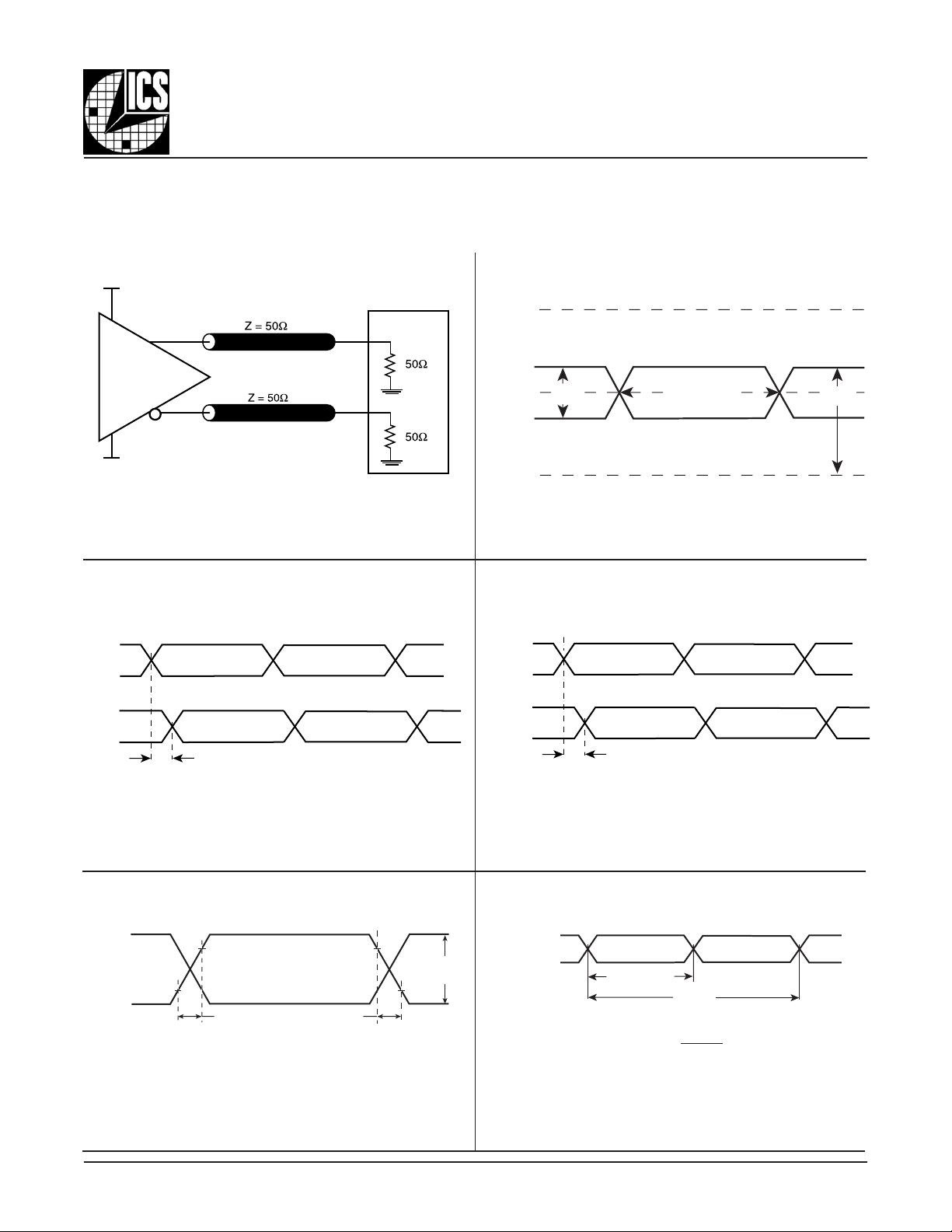
PARAMETER MEASUREMENT INFORMATION
Qx
nQx
SCOPE
ICS85356I
2:1, DIFFERENTIAL-TO-3.3V
DUAL LVPECL / ECL CLOCK MULTIPLEXER
V
CC
nCLKxA,
nCLKxB
CLKxA,
CLKxB
VPP
Cross Points
V
CMR
-1.3V ± 0.165V
3.3V OUTPUT LOAD AC TEST CIRCUIT
nQx
Qx
nQy
Qy
t
sk(o)
OUTPUT SKEW
V
EE
DIFFERENTIAL INPUT LEVEL
nCLKxA,
nCLKxB
CLKxA,
CLKxB
nQ0, nQ1
Q0, Q1
t
PD
PROPAGATION DELAY
nQ0, nQ1
Q0, Q1
Pulse Width
odc =
t
PERIOD
t
PW
t
PERIOD
Clock
Outputs
20%
80%
t
R
80%
t
F
20%
V
SWING
OUTPUT RISE/FALL TIME OUTPUT DUTY CYCLE/PULSE WIDTH/PERIOD
85356AMI www.icst.com/products/hiperclocks.html REV. A OCTOBER 7, 2004
5
Page 6

Integrated
Circuit
Systems, Inc.
DUAL LVPECL / ECL CLOCK MULTIPLEXER
APPLICATION INFORMATION
WIRING THE DIFFERENTIAL INPUT TO ACCEPT SINGLE ENDED LEVELS
Figure 2
single ended levels. The reference voltage V_REF = V
generated by the bias resistors R1, R2 and C1. This bias circuit
should be located as close as possible to the input pin. The ratio
shows how the differential input can be wired to accept
/2 is
CC
Single Ended Clock Input
of R1 and R2 might need to be adjusted to position the V_REF in
the center of the input voltage swing. For example, if the input
clock swing is only 2.5V and VCC = 3.3V, V_REF should be 1.25V
and R2/R1 = 0.609.
VCC
R1
1K
CLKx
ICS85356I
2:1, DIFFERENTIAL-TO-3.3V
V_REF
C1
0.1u R2
FIGURE 1. SINGLE ENDED S IGNAL DRIVING DIFFERENTIAL INPUT
TERMINATION FOR LVPECL OUTPUTS
The clock layout topology shown below is a typical termination for LVPECL outputs. The two different layouts mentioned
are recommended only as guidelines.
FOUT and nFOUT are low impedance follower outputs that generate ECL/LVPECL compatible outputs. Therefore, terminating
resistors (DC current path to ground) or current sources must
be used for functionality. These outputs are designed to drive
Z
= 50Ω
o
FOUT
= 50Ω
Z
o
RTT = Z
((V
OH
1
+ VOL) / (VCC – 2)) – 2
50Ω 50Ω
o
RTT
FIN
VCC - 2V
nCLKx
1K
50Ω transmission lines. Matched impedance techniques should
be used to maximize operating frequency and minimize signal
distortion.
Figures 2A and 2B
show two different layouts which
are recommended only as guidelines. Other suitable clock layouts may exist and it would be recommended that the board
designers simulate to guarantee compatibility across all printed
circuit and clock component process variations.
3.3V
125Ω 125Ω
= 50Ω
Z
o
FOUT FIN
= 50Ω
Z
o
84Ω 84Ω
FIGURE 2B. LVPECL OUTPUT TERMINATIONFIGURE 2A. LVPECL OUTPUT TERMINATION
85356AMI www.icst.com/products/hiperclocks.html REV. A OCTOBER 7, 2004
6
Page 7

Integrated
Circuit
Systems, Inc.
DIFFERENTIAL CLOCK INPUT INTERFACE
The CLK /nCLK accepts LVDS, LVPECL, LVHSTL, SSTL, HCSL
and other differential signals. Both V
V
and V
PP
input requirements. Figures 3A to 3E show inter-
CMR
face examples for the HiPerClockS CLK/nCLK input driven by
the most common driver types. The input interfaces suggested
and VOH must meet the
SWING
ICS85356I
2:1, DIFFERENTIAL-TO-3.3V
DUAL LVPECL / ECL CLOCK MULTIPLEXER
here are examples only. Please consult with the vendor of the
driver component to confirm the driver termination requirements.
For example in
Figure 3A,
HiPerClockS LVHSTL drivers. If you are using an LVHSTL driver
from another vendor, use their termination recommendation.
the input termination applies for ICS
1.8V
LVHSTL
ICS
HiPerClockS
LVHSTL Driver
Zo = 50 Ohm
Zo = 50 Ohm
R1
50
3.3V
CLK
nCLK
HiPerClockS
Input
R2
50
FIGURE 3A. HIPERCLOCKS CLK/nCLK INPUT DRIVEN BY
ICS HIPERCLOCKS LVHSTL DRIVER
3.3V
LVPECL
Zo = 50 Ohm
Zo = 50 Ohm
3.3V
R3
125
R4
125
R1
84
3.3V
CLK
nCLK
HiPerClockS
Input
R2
84
3.3V
LVPECL
Zo = 50 Ohm
Zo = 50 Ohm
R1
50
R3
50
3.3V
CLK
nCLK
HiPerClockS
Input
R2
50
FIGURE 3B. HIPERCLOCKS CLK/nCLK INPUT DRIVEN BY
3.3V LVPECL DRIVER
3.3V
3.3V
LVDS_D river
Zo = 50 Ohm
Zo = 50 Ohm
R1
100
CLK
nCLK
Receiver
FIGURE 3C. HIPERCLOCKS CLK/nCLK INPUT DRIVEN BY
3.3V LVPECL DRIVER
3.3V
CLK
nCLK
3.3V
HiPerClockS
Input
3.3V
LVPECL
R5
100 - 200
R5,R6 locate near the driver pin.
Zo = 50 Ohm
Zo = 50 Ohm
R6
100 - 200
R3
R4
125
C1
C2
125
R2
R1
84
84
FIGURE 3D. HIPERCLOCKS CLK/nCLK INPUT DRIVEN BY
3.3V LVDS DRIVER
FIGURE 3E. HIPERCLOCKS CLK/NCLK INPUT DRIVEN BY
3.3V LVPECL DRIVER WITH AC COUPLE
85356AMI www.icst.com/products/hiperclocks.html REV. A OCTOBER 7, 2004
7
Page 8

Integrated
Circuit
Systems, Inc.
2:1, DIFFERENTIAL-TO-3.3V
ICS85356I
DUAL LVPECL / ECL CLOCK MULTIPLEXER
POWER CONSIDERATIONS
This section provides information on power dissipation and junction temperature for the ICS85356I.
Equations and example calculations are also provided.
1. Power Dissipation.
The total power dissipation for the ICS85356I is the sum of the core power plus the power dissipated in the load(s).
The following is the power dissipation for V
NOTE: Please refer to Section 3 for details on calculating power dissipated in the load.
= 3.3V + 0.3V = 3.6V, which gives worst case results.
CC
• Power (core)
• Power (outputs)
If all outputs are loaded, the total power is 2 * 30.2mW = 60.4mW
Total Power
2. Junction Temperature.
Junction temperature, Tj, is the temperature at the junction of the bond wire and bond pad and directly affects the reliability of the
device. The maximum recommended junction temperature for HiPerClockS
The equation for Tj is as follows: Tj = θ
Tj = Junction Temperature
= Junction-to-Ambient Thermal Resistance
θ
JA
Pd_total = Total Device Power Dissipation (example calculation is in section 1 above)
= Ambient Temperature
T
A
In order to calculate junction temperature, the appropriate junction-to-ambient thermal resistance θ
moderate air flow of 200 linear feet per minute and a multi-layer board, the appropriate value is 39.7°C/W per Table 6A below.
Therefore, Tj for an ambient temperature of 85°C with all outputs switching is:
85°C + 0.204W * 39.7°C/W = 93.1°C. This is well below the limit of 125°C
This calculation is only an example. Tj will obviously vary depending on the number of loaded outputs, supply voltage, air flow,
and the type of board (single layer or multi-layer).
MAX
= V
MAX
_MAX
* I
CC_MAX
= 30.2mW/Loaded Output pair
= 3.6V * 40mA = 144mW
EE_MAX
(3.6V, with all outputs switching) = 144mW + 60.4mW = 204.4mW
TM
devices is 125°C.
* Pd_total + T
JA
A
must be used . Assuming a
JA
Table 6A. Thermal Resistance
θθ
θJA for 20-pin SOIC, Forced Convection
θθ
θθ
θJA by Velocity (Linear Feet per Minute)
θθ
0 200 500
Single-Layer PCB, JEDEC Standard Test Boards 83.2°C/W 65.7°C/W 57.5°C/W
Multi-Layer PCB, JEDEC Standard Test Boards 46.2°C/W 39.7°C/W 36.8°C/W
NOTE: Most modern PCB designs use multi-layered boards. The data in the second row pertains to most designs.
Table 6B. Thermal Resistance
θθ
θJA for 20-pin TSSOP, Forced Convection
θθ
θθ
θJA by Velocity (Linear Feet per Minute)
θθ
0 200 500
Single-Layer PCB, JEDEC Standard Test Boards 114.5°C/W 98.0°C/W 88.0°C/W
Multi-Layer PCB, JEDEC Standard Test Boards 73.2°C/W 66.6°C/W 63.5°C/W
NOTE: Most modern PCB designs use multi-layered boards. The data in the second row pertains to most designs.
85356AMI www.icst.com/products/hiperclocks.html REV. A OCTOBER 7, 2004
8
Page 9

Integrated
Circuit
Systems, Inc.
DUAL LVPECL / ECL CLOCK MULTIPLEXER
3. Calculations and Equations.
The purpose of this section is to derive the power dissipated into the load.
ICS85356I
2:1, DIFFERENTIAL-TO-3.3V
LVPECL output driver circuit and termination are shown in
Figure 4. LVPECL Driver Circuit and Termination
Figure 4.
VCC
Q1
V
OUT
RL = 50
V
- 2V
CC
To calculate worst case power dissipation into the load, use the following equations which assume a 50Ω load, and a termination voltage
of V
- 2V.
CC
• For logic high, V
(V
- V
CC_MAX
OH_MAX
• For logic low, V
(V
- V
CC_MAX
OL_MAX
OUT
)
= 1.0V
= V
OUT
)
= 1.7V
= V
Pd_H is power dissipation when the output drives high.
Pd_L is the power dissipation when the output drives low.
Pd_H = [(V
[(2V - 1V)/50Ω] * 1V = 20.0mW
Pd_L = [(V
[(2V - 1.7V)/50Ω] * 1.7V = 10.2mW
OH_MAX
OL_MAX
– (V
– (V
CC_MAX
CC_MAX
- 2V))/RL] * (V
- 2V))/RL] * (V
Total Power Dissipation per output pair = Pd_H + Pd_L = 30.2mW
85356AMI www.icst.com/products/hiperclocks.html REV. A OCTOBER 7, 2004
OH_MAX
OL_MAX
= V
= V
CC_MAX
CC_MAX
CC_MAX
CC_MAX
– 1.0V
– 1.7V
- V
OH_MAX
- V
OL_MAX
) = [(2V - (V
) = [(2V - (V
9
OH_MAX
OL_MAX
))
/RL] * (V
))
/RL] * (V
CC_MAX
CC_MAX
- V
- V
OH_MAX
OL_MAX
) =
) =
- V
_MAX
CC
- V
_MAX
CC
Page 10

Integrated
Circuit
Systems, Inc.
ICS85356I
2:1, DIFFERENTIAL-TO-3.3V
DUAL LVPECL / ECL CLOCK MULTIPLEXER
RELIABILITY INFORMATION
TABLE 7A. θ
Single-Layer PCB, JEDEC Standard Test Boards 83.2°C/W 65.7°C/W 57.5°C/W
Multi-Layer PCB, JEDEC Standard Test Boards 46.2°C/W 39.7°C/W 36.8°C/W
NOTE: Most modern PCB designs use multi-layered boards. The data in the second row pertains to most designs.
TABLE 7B. θ
Single-Layer PCB, JEDEC Standard Test Boards 114.5°C/W 98.0°C/W 88.0°C/W
Multi-Layer PCB, JEDEC Standard Test Boards 73.2°C/W 66.6°C/W 63.5°C/W
NOTE: Most modern PCB designs use multi-layered boards. The data in the second row pertains to most designs.
. AIR FLOW TABLE FOR 20 LEAD SOIC
VS
JA
θθ
θJA by Velocity (Linear Feet per Minute)
θθ
. AIR FLOW TABLE FOR 20 LEAD TSSOP
VS
JA
θθ
θJA by Velocity (Linear Feet per Minute)
θθ
0 200 500
0 200 500
TRANSISTOR COUNT
The transistor count for ICS85356I is: 446
85356AMI www.icst.com/products/hiperclocks.html REV. A OCTOBER 7, 2004
10
Page 11

Integrated
Circuit
Systems, Inc.
PACKAGE OUTLINE - M SUFFIX FOR 20 LEAD SOIC
ICS85356I
2:1, DIFFERENTIAL-TO-3.3V
DUAL LVPECL / ECL CLOCK MULTIPLEXER
T
ABLE 8A. PACKAGE DIMENSIONS
LOBMYS
N02
A--56.2
1A01.0--
2A50.255.2
B33.015.0
C81.023.0
D06.2100.31
E04.706.7
eCISAB72.1
H00.0156.01
h52
L04.072.1
α
Reference Document: JEDEC Publication 95, MS - 013, MO - 119
muminiMmumixaM
.057.0
°0°8
sretemilliM
85356AMI www.icst.com/products/hiperclocks.html REV. A OCTOBER 7, 2004
11
Page 12

Integrated
Circuit
Systems, Inc.
PACKAGE OUTLINE - G SUFFIX FOR 20 LEAD TSSOP
ICS85356I
2:1, DIFFERENTIAL-TO-3.3V
DUAL LVPECL / ECL CLOCK MULTIPLEXER
T
ABLE 8B. PACKAGE DIMENSIONS
LOBMYS
N02
A--02.1
1A50.051.0
2A08.050.1
b91.003.0
c90.002.0
D04.606.6
ECISAB04.6
1E03.405.4
eCISAB56.0
L5
α
aaa--01.0
REFERENCE DOCUMENT: JEDEC PUBLICATION 95, MO-153
muminiMmumixaM
4.057.0
°0°8
sretemilliM
85356AMI www.icst.com/products/hiperclocks.html REV. A OCTOBER 7, 2004
12
Page 13

Integrated
Circuit
Systems, Inc.
2:1, DIFFERENTIAL-TO-3.3V
DUAL LVPECL / ECL CLOCK MULTIPLEXER
TABLE 9. ORDERING INFORMATION
rebmuNredrO/traPgnikraMegakcaPtnuoCerutarepmeT
IMA65358SCIIMA65358SCICIOSdael02ebutrep83C°58otC°04-
IIMA65358SCIleeRdnaepaTnoCIOSdael020001C°58otC°04-
358SCIIGA65358SCIleeRdnaepaTnoPOSSTdael020052C°58otC°04-
TIMA65358SC
IGA65358SCIIGA65358SCIPOSSTdael02ebutrep27C°58otC°04-
TIGA65
FLIGA65358SCILIGA65358SCIPOSST"eerFdaeL"dael02ebutre
TFLIGA65358SCILIGA65358SCI
leeRdna
epaTnoPOSST"eerFdaeL"dael02
p27C°58otC°04-
ICS85356I
0052C°58otC°04-
The aforementioned trademark, HiPerClockS™ is a trademark of Integrated Circuit Systems, Inc. or its subsidiaries in the United States and/or other countries.
While the information presented herein has been checked for both accuracy and reliability, Integrated Circuit Systems, Incorporated (ICS) assumes no responsibility for either its use
or for infringement of any patents or other rights of third parties, which would result from its use. No other circuits, patents, or licenses are implied. This product is intended for use
in normal commercial and industrial applications. Any other applications such as those requiring high reliability, or other extraordinary environmental requirements are not
recommended without additional processing by ICS. ICS reserves the right to change any circuitry or specifications without notice. ICS does not authorize or warrant any ICS product
for use in life support devices or critical medical instruments.
85356AMI www.icst.com/products/hiperclocks.html REV. A OCTOBER 7, 2004
13
Page 14

Integrated
Circuit
Systems, Inc.
2:1, DIFFERENTIAL-TO-3.3V
ICS85356I
DUAL LVPECL / ECL CLOCK MULTIPLEXER
TEEHSYROTSIHNOISIVER
veRelbaTegaPegnahCfonoitpircseDetaD
7
A
31
.tamrofteehsataddetadpU
.noitcesecafretnItupnIkcolClaitnereffiDdeddA
ebmuntrapeerFdaeLdedda-elbaTnoitamrofnIgniredrO
.r
40/7/01
85356AMI www.icst.com/products/hiperclocks.html REV. A OCTOBER 7, 2004
14
 Loading...