

Page 1
查询ICS8431-21供应商
Integrated
Circuit
Systems, Inc.
GENERAL DESCRIPTION
ICS
HiPerClockS™
providing an output frequency range of 62.5MHz to 350MHz.
The output frequency can be programmed using the parallel interface, M0 through M8 to the configuration logic, and the output
divider control pin, DIV_SEL. Spread spectrum clocking is programmed via the control inputs SSC_CTL0 and SSC_CTL1.
Programmable features of the ICS8431-21 support four operational modes. The four modes are spread spectrum clocking (SSC), non-spread spectrum clock and two test modes
which are controlled by the SSC_CTL[1:0] pins. Unlike other
synthesizers, the ICS8431-21 can immediately change
spread-spectrum operation without having to reset the device.
In SSC mode, the output clock is modulated in order to achieve
a reduction in EMI. In one of the PLL bypass test modes, the
PLL is disconnected as the source to the differential output
allowing an external source to be connected to the TEST_I/O
pin. This is useful for in-circuit testing and allows the differential output to be driven at a lower frequency throughout the
system clock tree. In the other PLL bypass mode, the oscillator divider is used as the source to both the M and the Fout
divide by 2. This is useful for characterizing the oscillator and
internal dividers.
The ICS8431-21 is a general purpose clock frequency synthesizer for IA64/32 application and a
member of the HiPerClockS™ family of High Performance Clock Solutions from ICS. The VCO operates at a frequency range of 250MHz to 700MHz
ICS8431-21
350MHZ, LOW JITTER, CRYSTAL OSCILLATOR-
TO-3.3V LVPECL FREQUENCY SYNTHESIZER
FEATURES
• Fully integrated PLL
• Differential 3.3V LVPECL output
• Crystal oscillator interface
• Output frequency range: 62.5MHz to 350MHz
• Crystal input frequency range: 14MHz to 25MHz
• VCO range: 250MHz to 700MHz
• Programmable PLL loop divider for generating a variety
of output frequencies
• Spread Spectrum Clocking (SSC) fixed at 1/2% modulation
for environments requiring ultra low EMI
• PLL bypass modes supporting in-circuit testing and on-chip
functional block characterization
• Cycle-to-cycle jitter: 30ps (maximum)
• 3.3V supply voltage
• 0°C to 85°C ambient operating temperature
• Replaces ICS8431-01 and ICS8431-11
• Lead-Free package fully RoHS compliant
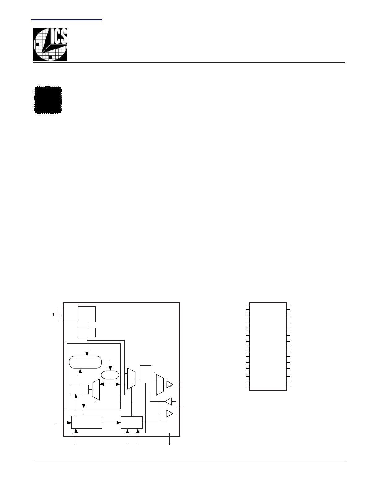
BLOCK DIAGRAM PIN ASSIGNMENT
nP_LOAD
M0
V
M1
M2
M3
M4
M5
M6
M7
M8
V
1
2
3
4
5
6
7
8
9
10
11
12
EE
13
14
CC
XTAL_IN
XTAL_OUT
OSC
÷ 16
PHASE
DETECTOR
÷ M
PLL
VCO
÷2
÷4
FOUT
nFOUT
SSC_CTL0
SSC_CTL1
TEST_I/O
ICS8431-21
TEST_I/O
M0:M8
8431AM-21 www.icst.com/products/hiperclocks.html REV. A APRIL 27, 2005
Configuration
Logic
nP_LOAD
SSC_CTL0
SSC
Control
Logic
SSC_CTL1
DIV_SEL
1
7.5mm x 18.05mm x 2.25mm package body
28-Lead SOIC
M Package
Top View
28
27
26
25
24
23
22
21
20
19
18
17
16
15
V
CC
XTAL_IN
XTAL_OUT
nc
nc
V
CCA
VEE
MR
DIV_SEL
V
CCO
FOUT
nFOUT
V
EE
Page 2

Integrated
Circuit
Systems, Inc.
FUNCTIONAL DESCRIPTION
The ICS8431-21 features a fully integrated PLL and therefore
requires no external components for setting the loop bandwidth.
The output of the oscillator is divided by 16 prior to the phase
detector. With a 16MHz crystal this provides a 1MHz reference
frequency. The VCO of the PLL operates over a range of 250MHz
to 700MHz. The output of the M divider is also applied to the phase
detector.
ICS8431-21
350MHZ, LOW JITTER, CRYSTAL OSCILLATOR-
TO-3.3V LVPECL FREQUENCY SYNTHESIZER
The PLL loop divider or M divider is programmed by using
inputs M0 through M8. While the nP_LOAD input is held LOW,
the data present at M0:M8 is transparent to the M divider. On
the LOW-to-HIGH transition of nP_LOAD, the M0:M8 data is
latched into the M divider and any further changes at the
M0:M8 inputs will not be seen by the M divider until the next
LOW transition on nP_LOAD.
The phase detector and the M divider force the VCO output
frequency to be M times the reference frequency by adjusting
the VCO control voltage. Note that for some values of M (either too high or too low), the PLL will not achieve lock. The
output of the VCO is scaled by a divider prior to being sent to
the LVPECL output buffer. The divider provides a 50% output
duty cycle.
The programmable features of the ICS8431-21 support four
output operational modes and a programmable M divider and
output divider. The four output operational modes are spread
spectrum clocking (SSC), non-spread spectrum clock and
two test modes and are controlled by the SSC_CTL[1:0] pins.
The relationship between the VCO frequency, the crystal frequency and the M divider is defined as follows:
fxtal
fVCO =
The M value and the required values of M0:M8 for programming
FOUT
Table 3B
fVCO
=
the VCO are shown in
Function Table. The frequency out is defined as follows:
For the ICS8431-21, the output divider may be set to either ÷2
or ÷4 by the DIV_SEL pin. For an input of 16 MHz, valid
M values for which the PLL will achieve lock are defined as:
250 ≤ M ≤ 511.
x
M
16
, Programmable VCO Frequency
fxtal x M
=
N
16 x N
8431AM-21 www.icst.com/products/hiperclocks.html REV. A APRIL 27, 2005
2
Page 3
Integrated
Circuit
Systems, Inc.
TABLE 1. PIN DESCRIPTIONS
rebmuNemaNepyTnoitpircseD
,4,3,2,1
7,6,5
9,88M-7MtupnIpulluP
11,01
12,51,21V
31O/ITSET
72,41V
71,61TUOF,TUOFntuptuO .slevelecafretniLCEPVLV3.3.rezisehtnysehtrofstuptuolaitnereffiD
8
1V
91LES_VIDtupnInwodlluP
02RMtupnInwodlluP
22V
42,32cndesunU.tcennocoN
62,52
82DAOL_PntupnInwodlluP
pulluP
:ETON
6M-0MtupnInwodlluP
,0LTCCSS
1LTCCSS
EE
CC
OCC
ACC
,TUO_LATX
NI_LATX
dna
ICS8431-21
350MHZ, LOW JITTER, CRYSTAL OSCILLATOR-
TO-3.3V LVPECL FREQUENCY SYNTHESIZER
noitisnartHGIH-ot-WOLnodehctalataD.stupniredividM
slevelecafretnisnipLTTVL/SOMCVL.tupniDAOL_Pnfo
.
tupnIpulluP.sleveleca
rewoPVllatcennoC.snipylppusevitageN
/tupnI
tuptuO
rewoP.nipylppuseroC
rewoP.nipylppustuptuO
MCVL
.slevelecafretniLTTVL/SO
rewoP.nipylppusgolanA
tupnI
csolatsyrC
.tuptuoehtsiTUO_LATX
nwodlluP
fretniSOMCVL/LTTVL.sniplortnocCCS
EE
.dnuorgdraobotsnip
.elbaTnoitcnuFA3elbaTnidenifedsademmargorP
.TUOFrofeulavedividtuptuoehtsenimreteD
erasredividlanretnieht,HGIHcigolnehW.teseRretsaMhgiHevitcA
otTUOFtuptuoeurtehtgnisuacteser
tuptuodetrevniehtdnawolog
ehtdnasredividlanretnieht,WOLcigolnehW.hgihogotTUOFn
onseodRMfonoitressA.delbaneerastuptuo
TdnaMdedaoltceffet
.slevelecafretniLTTVL/SOMCVL.seulav
.tupniehtsiNI_LATX.ecafretnirotalli
0M:8MtatneserpatadnehwsenimreteD.tupnidaollellaraP
levelecafretniSOMCVL/LTTVL.redividMotnidedaolsi
.s
.seulavlacipytrof,scitsiretcarahCniP,2elbaTeeS.srotsisertupnilanretniotrefer
TABLE 2. PIN CHARACTERISTICS
lobmySretemaraPsnoitidnoCtseTmuminiMlacipyTmumixaMstinU
C
NI
R
PULLUP
R
8431AM-21 www.icst.com/products/hiperclocks.html REV. A APRIL 27, 2005
NWODLLUP
ecnaticapaCniPtupnI 4Fp
rotsiseRpulluPtupnI 15kΩ
rotsiseRnwodlluPtupnI 15kΩ
3
Page 4
Integrated
Circuit
Systems, Inc.
TABLE 3A. SSC CONTROL INPUT FUNCTION TABLE
ICS8431-21
350MHZ, LOW JITTER, CRYSTAL OSCILLATOR-
TO-3.3V LVPECL FREQUENCY SYNTHESIZER
stupnI
1LTC_CSS0LTC_CSS
00 lanretn
01LLPdelbanE
10 lanretxEdelbasiDklCtseTklCtseTtupnI
11 LLPdelbasiD
U:1ETON
O/I_TSET
ecruoS
IdelbasiDLATXf ÷ 23LATXf ÷ 46
CSS
0LES_VID1LES_VID
MxLATXf
23
MxLATXf
23
.noitaziretcarahcdnagubedesuohnirofdes
TUOFn,TUOF
ATXf
46
46
TABLE 3B. PROGRAMMABLE VCO FREQUENCY FUNCTION TABLE (NOTE 1)
ycneuqerFOCV
)zHM(
052052 0 11111010
152152 0 11111011
252252 0 11111100
352352 0 11111101
• • •••••••••
• • •••••••••
805805 111111100
905905 111111101
015015 111111110
115115 111111111
sA:1ETON
tnuoCM
6528214623618421
8M7M6M5M4M3M2M1M0M
.latsyrczHM61asemus
stuptuO
O/I_TSET
LATXf ÷ 61
÷ M
MxL
MxLATXf
Z-iH
( ≤ klCtseT ≤ )zHM002
Z-iHnoitaludoMCSSoN
zHM1
sedoMlanoitarepO
NdnaM,rotallicso;ssapybLLP
1ETON.edomtsetsredivid
;CSStluafeD
tnecreP½=rotcaFnoitaludoM
;1ETON,edoMssapyBLLP
TABLE 3C. FUNCTION TABLE
stupnI
LES_VIDmuminiMmumixaM
02 521053
14 5.26571
8431AM-21 www.icst.com/products/hiperclocks.html REV. A APRIL 27, 2005
eulaVrediviDN
)zHM(ycneuqerFtuptuO
4
Page 5
Integrated
Circuit
Systems, Inc.
ABSOLUTE MAXIMUM RATINGS
ICS8431-21
350MHZ, LOW JITTER, CRYSTAL OSCILLATOR-
TO-3.3V LVPECL FREQUENCY SYNTHESIZER
Supply Voltage, V
Inputs, V
I
Outputs, I
Continuous Current 50mA
CC
O
4.6V
-0.5V to V
+ 0.5V
CC
Surge Current 100mA
Package Thermal Impedance, θ
Storage Temperature, T
STG
TABLE 4A. POWER SUPPLY DC CHARACTERISTICS, V
46.2°C/W (0 lfpm)
JA
-65°C to 150°C
CC
= V
lobmySretemaraPsnoitidnoCtseTmuminiMlacipyTmumixaMstinU
V
CC
V
OCC
V
ACC
I
EE
I
ACC
egatloVylppuSeroC 531.33.3564.3V
egatloVylppuStuptuO 531.33.3564.3V
egatloVylppuSgolanA 531.33.3564.3V
tnerruCylppuSrewoP 551Am
tnerruCylppuSgolanA 61Am
TABLE 4B. LVCMOS / LVTTL DC CHARACTERISTICS, V
lobmySretemaraPsnoitidnoCtseTmuminiMlacipyTmumixaMstinU
,0LTC_CSS,8M:0M
V
HI
egatloVhgiHtupnI
DAOL_Pn
V
LI
egatloVwoLtupnI
DAOL_Pn
I
HI
I
LI
tnerruChgiHtupnI
tnerruCwoLtupnI
,RM,1LTC_CSS
,O/I_TSET,LES_VID
,0LTC_CSS,8M:0M
,RM,1LTC_CSS
,O/I_TSET,LES_VID
,0LTC_CSS,8M,7M
OI_TSET,1LTC_CSS
LES_VID,6M:0M
RM,DAOL_Pn
,0LTC_CSS,8M,7M
OI_TSET,1LTC_CSS
LES_VID,6M:0M
RM,DAOL_Pn
CC
CCA
= V
V
V
NOTE: Stresses beyond those listed under Absolute
Maximum Ratings may cause permanent damage to the
device. These ratings are stress specifications only. Functional
operation of product at these conditions or any conditions beyond those listed in the
istics
is not implied. Exposure to absolute maximum rating
DC Characteristics
or
conditions for extended periods may affect product reliability.
= V
= 3.3V±5%, TA = 0°C TO 85°C
CCO
= V
CCA
= 3.3V±5%, TA = 0°C TO 85°C
CCO
2V
CC
3.0-8.0V
V
V=
CC
NI
V=
V
CC
NI
CC
CC
V564.3=5Aµ
V564.3=051Aµ
V,V564.3=
V0=051-Aµ
NI
V,V564.3=
V0=5-Aµ
NI
AC Character-
3.0+V
TABLE 4C. LVPECL DC CHARACTERISTICS, V
CC
= V
CCA
= V
= 3.3V±5%, TA = 0°C TO 85°C
CCO
lobmySretemaraPsnoitidnoCtseTmuminiMlacipyTmumixaMstinU
V
HO
V
LO
V
GNIWS
8431AM-21 www.icst.com/products/hiperclocks.html REV. A APRIL 27, 2005
egatloVwoLtuptuO1ETON;V
1ETON;egatloVhgiHtuptuOV
4.1-V
OCC
0.2-V
OCC
9.0-V
OCC
7.1-V
OCC
gniwSegatloVtuptuOkaeP-ot-kaeP6.00.1V
05htiwdetanimrettuptuO:1ETON Ω Vot
OCC
5
.tiucriCtseTdaoLtuptuOV3.3,noitceStnemerusaeMretemaraPeeS.V2-
Page 6
Integrated
Circuit
Systems, Inc.
TABLE 5. CRYSTAL CHARACTERISTICS
retemaraPsnoitidnoCtseTmuminiMlacipyTmumixaMstinU
noitallicsOfoedoM latnemadnuF
ycneuqerF 416152zHM
RseireStnelaviuqE 04
ecnaticapaCtnuhS 37Fp
ICS8431-21
350MHZ, LOW JITTER, CRYSTAL OSCILLATOR-
TO-3.3V LVPECL FREQUENCY SYNTHESIZER
)RSE(ecnatsise
Ω
TABLE 6. AC CHARACTERISTICS, V
CC
= V
CCA
= V
= 3.3V±5%, TA = 0°C TO 85°C
CCO
lobmySretemaraPsnoitidnoCtseTmuminiMlacipyTmumixaMstinU
F
TUO
t
j)cc(ti
ycneuqerFtuptuO 5.26053zHM
5,1ETON;rettiJelcyC-ot-elcyCF
≥ zHM0019103sp
TUO
cdoelcyCytuDtuptuO 840525%
t
Rt/F
F
F
F
t
latx
M
FM
CSS
der
ELBATS
emiTllaF/esiRtuptuO%08ot%02002007sp
3,2ETON;egnaRtupnIlatsyrC 416152zHM
4ETON;ycneuqerFnoitaludoMCSSF
4ETON;rotcaFnoitaludoMCSSF
;noitcudeRlartcepS4ETONF
TUO
TUO
TUO
zHM002=9233.33zHK
zHM002=4.06.0%
zHM002=701Bd
tuptuOkcolCelbatSotpu-rewoP 01sm
.noitcesnoitamrofnItnemerusaeMretemaraPehtniserugiFeeS
cnamrofreprettiJ:1ETON
.stupniLATXgnisue
.egnargnitarepoOCVehtnihtiwdilavylnO:2ETON
3ETON
.etoNnoitacilppAotrefer,tupniLATXroF:
:4ETON.delbanegnikcolcmurtcepSdaerpS
.56dradnatSCEDEJhtiwecnadroccanidenifedsiretemarapsihT:5ETON
8431AM-21 www.icst.com/products/hiperclocks.html REV. A APRIL 27, 2005
6
Page 7

2V
Integrated
Circuit
Systems, Inc.
PARAMETER MEASUREMENT INFORMATION
ICS8431-21
350MHZ, LOW JITTER, CRYSTAL OSCILLATOR-
TO-3.3V LVPECL FREQUENCY SYNTHESIZER
VCC,
V
, V
CCA
CCO
LVPECL
V
EE
-1.3V ± 0.165V
3.3V OUTPUT LOAD AC TEST CIRCUIT
80%
Clock
Outputs
20%
t
R
Qx
nQx
80%
t
F
SCOPE
V
SWI NG
20%
nFOUT
FOUT
➤
t
cycle n
t
jit(cc) = tcycle n –tcycle n+1
CYCLE-TO-CYCLE JITTER
nFOUT
FOUT
Pulse Width
1000 Cycles
t
PERIOD
t
odc =
t
PERIOD
➤
t
➤
PW
cycle n+1
➤
OUTPUT RISE/FALL TIME
8431AM-21 www.icst.com/products/hiperclocks.html REV. A APRIL 27, 2005
OUTPUT DUTY CYCLE/PULSE WIDTH/PERIOD
7
Page 8

Integrated
Circuit
Systems, Inc.
APPLICATION INFORMATION
POWER SUPPLY FILTERING T ECHNIQUES
As in any high speed analog circuitry, the power supply pins
are vulnerable to random noise. The ICS8431-21 provides
separate power supplies to isolate any high switching noise
, V
from the outputs to the internal PLL. V
, and V
CC
CCA
be individually connected to the power supply plane through
vias, and bypass capacitors should be used for each pin. To
achieve optimum jitter performance, better power supply isolation is required.
Figure 3
illustrates how a 10Ω along with a
10μF and a .01μF bypass capacitor should be connected to
each V
CCA
pin.
CCO
should
ICS8431-21
350MHZ, LOW JITTER, CRYSTAL OSCILLATOR-
TO-3.3V LVPECL FREQUENCY SYNTHESIZER
3.3V
V
CC
.01μF
V
CCA
.01μF
FIGURE 3. POWER SUPPLY FILTERING
10Ω
10μF
TERMINATION FOR LVPECL OUTPUTS
The clock layout topology shown below is typical for
IA64/32 platforms. The two different layouts mentioned are
recommended only as guidelines.
FOUT and nFOUT are low impedance follower outputs that
generate ECL/LVPECL compatible outputs. Therefore, terminating resistors (DC current path to ground) or current sources
must be used for functionality. These outputs are designed to
Z
= 50Ω
o
FOUT
= 50Ω
Z
o
RTT = Z
((V
OH
1
+ VOL) / (VCC – 2)) – 2
50Ω 50Ω
o
RTT
FIN
VCC - 2V
drive 50Ω transmission lines. Matched impedance techniques
should be used to maximize operating frequency and minimize
signal distortion.
Figures 2A and 2B
show two different layouts
which are recommended only as guidelines. Other suitable clock
layouts may exist and it would be recommended that the board
designers simulate to guarantee compatibility across all printed
circuit and clock component process variations.
3.3V
125Ω 125Ω
= 50Ω
Z
o
FOUT FIN
= 50Ω
Z
o
84Ω 84Ω
FIGURE 2B. LVPECL OUTPUT TERMINATIONFIGURE 2A. LVPECL OUTPUT TERMINATION
8431AM-21 www.icst.com/products/hiperclocks.html REV. A APRIL 27, 2005
8
Page 9

Integrated
Circuit
Systems, Inc.
CRYSTAL INPUT INTERFACE
The ICS8431-21 has been characterized with 18pF parallel resonant
crystals. The capacitor values, C1 and C2, shown in
were determined using a 25MHz, 18pF parallel resonant crystal and
Figure 3
below
C1
22p
18pF Parallel Crystal
X1
C2
22p
Figure 3. CRYSTAL INPUT INTERFACE
ICS8431-21
350MHZ, LOW JITTER, CRYSTAL OSCILLATOR-
TO-3.3V LVPECL FREQUENCY SYNTHESIZER
were chosen to minimize the ppm error. The optimum C1 and C2
values can be slightly adjusted for different board layouts.
XTAL_OUT
XTAL_IN
SPREAD SPECTRUM
Spread-spectrum clocking is a frequency modulation technique for EMI reduction. When spread-spectrum is enabled,
a 30kHz triangle waveform is used with 0.5% down-spread
(+0.0% / -0.5%) from the nominal 200MHz clock frequency.
An example of a triangle frequency modulation profile is shown
Figure 4A
in
• Fnom = Nominal Clock Frequency in Spread OFF mode
(200MHz with 16MHz IN)
• Fm = Nominal Modulation Frequency (30kHz)
• δ = Modulation Factor (0.5% down spread)
(1 - δ) fnom + 2 fm x δ x fnom x t when 0 < t < ,
(1 - δ) fnom - 2 fm x δ x fnom x t when < t <
(1 - δ) Fnom
below. The ramp profile can be expressed as:
1
2 fm
➤
Fnom
1
2 fm
1
fm
The ICS8431-21 triangle modulation frequency deviation will
not exceed 0.6% down-spread from the nominal clock frequency (+0.0% / -0.5%). An example of the amount of down
spread relative to the nominal clock frequency can be seen in
the frequency domain, as shown in
this width to the fundamental frequency is typically 0.4%, and
will not exceed 0.6%. The resulting spectral reduction will be
greater than 7dB, as shown in
note the ICS8431-21 7dB minimum spectral reduction is the
component-specific EMI reduction, and will not necessarily
be the same as the system EMI reduction.
B
➤
δ = .4%
➤
Figure 4B.
Figure 4B
Δ − 10 dBm
A
The ratio of
. It is important to
➤
0.5/fm 1/fm
FIGURE 4A. TRIANGLE FREQUENCY MODULATION
8431AM-21 www.icst.com/products/hiperclocks.html REV. A APRIL 27, 2005
FIGURE 4B. 200MHZ CLOCK OUTPUT IN FREQUENCY DOMAIN
(A) SPREAD-SPECTRUM OFF (B) SPREAD-SPECTRUM ON
9
Page 10

Integrated
Circuit
Systems, Inc.
LAYOUT GUIDELINE
The schematic of the ICS8431-21 layout example used in this
layout guideline is shown in
Figure 5A.
ommended PCB board layout for this example is shown in
The ICS8431-21 rec-
ICS8431-21
350MHZ, LOW JITTER, CRYSTAL OSCILLATOR-
TO-3.3V LVPECL FREQUENCY SYNTHESIZER
Figure 5B.
The layout in the actual system will depend on the selected
component types and the density of the P.C. board.
VCC=3.3V
SP=Spare, not installed
This layout example is used as a general guideline.
Logic Input Pin Examples
VCC
Set Logic
Input t o
'1'
VCC
Set Logic
Input t o
'0'
VCC
U1
1
M0
2
M1
3
M2
4
M3
5
M4
6
M5
7
M6
8
M7
9
M8
10
SSC_CTL0
11
SSC_CTL1
12
VEE
13
TEST_IO
14 15
VCC VEE
C1
0.1uF
ICS8431-21
nP_LOAD
XTA L _O U T
DIV_SEL
VCC
XTAL_IN
NC
NC
VCC A
VEE
MR
VCC O
FOUT
nFOU T
VCC
28
27
26
25
24
23
22
21
20
19
18
17
16
VCC
C6
0.01uF
X1
VCC A
C3
0.01uF
C2
0.1uF
C8 22pF
C7 22pF
C4
10uF
FIGURE 5A. SCHEMATIC EXAMPLE
R5
VCC
10
Zo = 50 Ohm
Zo = 50 Ohm
RU1
1K
RD1
SP
To Logic
Input
pins
VCC
R1
125
R2
84
R3
125
R4
84
RU2
SP
RD2
1K
To Logic
Input
pins
+
-
8431AM-21 www.icst.com/products/hiperclocks.html REV. A APRIL 27, 2005
10
Page 11

Integrated
Circuit
Systems, Inc.
ICS8431-21
350MHZ, LOW JITTER, CRYSTAL OSCILLATOR-
TO-3.3V LVPECL FREQUENCY SYNTHESIZER
The following component footprints are used in this layout
example:
All the resistors and capacitors are size 0603.
POWER AND GROUNDING
Place the decoupling capacitors C1, C2 and C6, as close as
possible to the power pins. If space allows, placment of the
decoupling capacitor on the component side is preferred. This
can reduce unwanted inductance between the decoupling capacitor and the power pin generated by the via.
Maximize the power and ground pad sizes and number of vias
capacitors. This can reduce the inductance between the power
and ground planes and the component power and ground pins.
The RC filter consisting of R5, C3, and C4 should be placed as
close to the V
pin as possible.
CCA
CLOCK TRACES AND TERMINATION
Poor signal integrity can degrade the system performance or
cause system failure. In synchronous high-speed digital systems,
the clock signal is less tolerant to poor signal integrity than other
signals. Any ringing on the rising or falling edge or excessive ring
back can cause system failure. The shape of the trace and the
trace delay might be restricted by the available space on the board
and the component location. While routing the traces, the clock
signal traces should be routed first and should be locked prior to
routing other signal traces.
• The 50Ω output trace pair should have same length.
• Avoid sharp angles on the clock trace. Sharp angle turns
cause the characteristic impedance to change on the
transmission lines.
• Keep the clock traces on the same layer. Whenever possible, avoid placing vias on the clock traces. Placement
of vias on the traces can affect the trace characteristic
impedance and hence degrade signal integrity.
• To prevent cross talk, avoid routing other signal traces in
parallel with the clock traces. If running parallel traces is
unavoidable, allow a separation of at least three trace
widths between the differential clock trace and the other
signal trace.
• Make sure no other signal traces are routed between the
clock trace pair.
• The matching termination resistors should be located as
close to the receiver input pins as possible.
The matching termination resistors R1, R2, R3 and R4 should
be located as close to the receiver input pins as possible.
Other termination scheme can also be used but is not shown
in the example.
CRYSTAL
The crystal X1 should be located as close as possible to the pins
25 (XTAL_OUT) and 26 (XTAL_IN). The trace length between the
X1 and U1 should be kept to a minimum to avoid unwanted parasitic inductance and capacitance. Other signal traces should not
be routed near the crystal traces.
C8
GND
U1
ICS8431-21
C6
X1
C3
C1
C4
R5
C7
C2
Zo=50 Ohm
Zo=50 Ohm
VCC
Signals
VIA
FIGURE 5B. PCB BOARD LAYOUT FOR ICS8431-21
8431AM-21 www.icst.com/products/hiperclocks.html REV. A APRIL 27, 2005
11
Page 12

Integrated
Circuit
Systems, Inc.
350MHZ, LOW JITTER, CRYSTAL OSCILLATOR-
ICS8431-21
TO-3.3V LVPECL FREQUENCY SYNTHESIZER
POWER CONSIDERATIONS
This section provides information on power dissipation and junction temperature for the ICS8431-21.
Equations and example calculations are also provided.
1. Power Dissipation.
The total power dissipation for the ICS8431-21 is the sum of the core power plus the power dissipated in the load(s).
The following is the power dissipation for V
NOTE: Please refer to Section 3 for details on calculating power dissipated in the load.
= 3.3V + 5% = 3.465V, which gives worst case results.
CC
• Power (core)
• Power (outputs)
If all outputs are loaded, the total power is 1 * 30mW = 30mW
Total Power
= V
MAX
MAX
(3.465V, with all outputs switching) = 537.1mW + 30mW = 567.1mW
_MAX
* I
CC_MAX
= 30mW/Loaded Output pair
= 3.465V * 155mA = 537.1mW
EE_MAX
2. Junction Temperature.
Junction temperature, Tj, is the temperature at the junction of the bond wire and bond pad and directly affects the reliability of the
device. The maximum recommended junction temperature for HiPerClockS
The equation for Tj is as follows: Tj = θ
Tj = Junction Temperature
= Junction-to-Ambient Thermal Resistance
θ
JA
Pd_total = Total Device Power Dissipation (example calculation is in section 1 above)
= Ambient Temperature
T
A
In order to calculate junction temperature, the appropriate junction-to-ambient thermal resistance θ
moderate air flow of 200 linear feet per minute and a multi-layer board, the appropriate value is 39.7°C/W per Table 7 below.
Therefore, Tj for an ambient temperature of 85°C with all outputs switching is:
85°C + 0.567W * 39.7°C/W = 107.5°C. This is below the limit of 125°C.
This calculation is only an example. Tj will obviously vary depending on the number of loaded outputs, supply voltage, air flow,
and the type of board (single layer or multi-layer).
* Pd_total + T
JA
A
TM
devices is 125°C.
must be used. Assuming a
JA
Table 7. THERMAL RESISTANCE
θθ
θJA FOR 28-PIN SOIC, FORCED CONVECTION
θθ
θθ
θJA by Velocity (Linear Feet per Minute)
θθ
0 200 500
Single-Layer PCB, JEDEC Standard Test Boards 76.2°C/W 60.8°C/W 53.2°C/W
Multi-Layer PCB, JEDEC Standard Test Boards 46.2°C/W 39.7°C/W 36.8°C/W
NOTE: Most modern PCB designs use multi-layered boards. The data in the second row pertains to most designs.
8431AM-21 www.icst.com/products/hiperclocks.html REV. A APRIL 27, 2005
12
Page 13

Integrated
Circuit
Systems, Inc.
350MHZ, LOW JITTER, CRYSTAL OSCILLATOR-
TO-3.3V LVPECL FREQUENCY SYNTHESIZER
3. Calculations and Equations.
The purpose of this section is to derive the power dissipated into the load.
ICS8431-21
LVPECL output driver circuit and termination are shown in
FIGURE 6. LVPECL DRIVER CIRCUIT AND TERMINATION
Figure 6.
V
CCO
Q1
RL
50
V
CCO
V
OUT
- 2V
To calculate worst case power dissipation into the load, use the following equations which assume a 50Ω load, and a termination
voltage of V
• For logic high, V
• For logic low, V
Pd_H is power dissipation when the output drives high.
Pd_L is the power dissipation when the output drives low.
Pd_H = [(V
[(2V - 0.9V)/50Ω] * 0.9V = 19.8mW
Pd_L = [(V
[(2V - 1.7V)/50Ω] * 1.7V = 10.2mW
Total Power Dissipation per output pair = Pd_H + Pd_L = 30mW
CCO
(V
CCO_MAX
(V
CCO_MAX
OH_MAX
OL_MAX
- 2V.
– (V
- V
- V
– (V
OUT
OH_MAX
OUT
OL_MAX
CCO_MAX
CCO_MAX
= V
)
= 0.9V
= V
)
= 1.7V
- 2V))/RL] * (V
- 2V))/RL] * (V
OH_MAX
OL_MAX
= V
= V
CCO_MAX
CCO_MAX
CCO_MAX
CCO_MAX
– 0.9V
– 1.7V
- V
- V
OH_MAX
OL_MAX
) = [(2V - (V
) = [(2V - (V
CCO
CCO
_MAX
_MAX
- V
- V
OH_MAX
OL_MAX
))
/RL] * (V
))
/RL] * (V
CCO_MAX
CCO_MAX
- V
- V
OH_MAX
OL_MAX
) =
) =
8431AM-21 www.icst.com/products/hiperclocks.html REV. A APRIL 27, 2005
13
Page 14

Integrated
Circuit
Systems, Inc.
ICS8431-21
350MHZ, LOW JITTER, CRYSTAL OSCILLATOR-
TO-3.3V LVPECL FREQUENCY SYNTHESIZER
RELIABILITY INFORMATION
TABLE 8. θ
TRANSISTOR COUNT
The transistor count for ICS8431-21 is: 4790
VS. AIR FLOW TABLE FOR 28 LEAD SOIC
JA
θθ
θJA by Velocity (Linear Feet per Minute)
θθ
0 200 500
Single-Layer PCB, JEDEC Standard Test Boards 76.2°C/W 60.8°C/W 53.2°C/W
Multi-Layer PCB, JEDEC Standard Test Boards 46.2°C/W 39.7°C/W 36.8°C/W
NOTE: Most modern PCB designs use multi-layered boards. The data in the second row pertains to most designs.
8431AM-21 www.icst.com/products/hiperclocks.html REV. A APRIL 27, 2005
14
Page 15

Integrated
Circuit
Systems, Inc.
PACKAGE OUTLINE - M SUFFIX FOR 28 LEAD SOIC
ICS8431-21
350MHZ, LOW JITTER, CRYSTAL OSCILLATOR-
TO-3.3V LVPECL FREQUENCY SYNTHESIZER
T
ABLE 9. PACKAGE DIMENSIONS
LOBMYS
N82
A--56.2
1A01.0--
2A50.255.2
B33.015.0
C81.023.0
D07.7104.81
E04.706.7
eCISAB72.1
H00.0156.01
h52
L04.072.1
α
Reference Document: JEDEC Publication 95, MS-013, MO-119
MUMINIMMUMIXAM
.057.0
°0°8
sretemilliM
8431AM-21 www.icst.com/products/hiperclocks.html REV. A APRIL 27, 2005
15
Page 16

Integrated
Circuit
Systems, Inc.
TABLE 10. ORDERING INFORMATION
rebmuNredrO/traPgnikraMegakcaPgnigakcaPgnippihSerutarepmeT
12-MA1348SCI12-MA1348SCICIOSdaeL82ebuTC°58otC°0
T12-
MA1348SCI12-MA1348SCICIOSdaeL82leeR&epaT0001C°58otC°0
FL12-MA1348SCIDBTCIOS"eerF-daeL"daeL82ebuTC°58otC°0
TFL12
-MA1348SCIDBTCIOS"eerF-daeL"daeL82leeR&epaT0001C°58otC°0
ICS8431-21
350MHZ, LOW JITTER, CRYSTAL OSCILLATOR-
TO-3.3V LVPECL FREQUENCY SYNTHESIZER
muntrapehtotxiffus"FL"nahtiwderedroeratahtstraP:ETON
.tnailpmocSHoReradnanoitarugifnoceerF-bPehterareb
The aforementioned trademark, HiPerClockS™ is a trademark of Integrated Circuit Systems, Inc. or its subsidiaries in the United States and/or other countries.
While the information presented herein has been checked for both accuracy and reliability, Integrated Circuit Systems, Incorporated (ICS) assumes no responsibility for either its use
or for infringement of any patents or other rights of third parties, which would result from its use. No other circuits, patents, or licenses are implied. This product is intended for use
in normal commercial applications. Any other applications such as those requiring extended temperature range, high reliability, or other extraordinary environmental requirements are
not recommended without additional processing by ICS. ICS reserves the right to change any circuitry or specifications without notice. ICS does not authorize or warrant any ICS
product for use in life support devices or critical medical instruments.
8431AM-21 www.icst.com/products/hiperclocks.html REV. A APRIL 27, 2005
16
Page 17

Integrated
Circuit
Systems, Inc.
350MHZ, LOW JITTER, CRYSTAL OSCILLATOR-
ICS8431-21
TO-3.3V LVPECL FREQUENCY SYNTHESIZER
TEEHSYROTSIHNOISIVER
veRelbaTegaPegnahCfonoitpircseDetaD
A
01T
1
61
itceSserutaeF
tellubeerF-daeLdnatellubtnemecalperdedda-no
.rebmuntrapeerF-daeLdedda-elbaTnoitamrofnIgniredrO
50/72/4
8431AM-21 www.icst.com/products/hiperclocks.html REV. A APRIL 27, 2005
17
 Loading...