

Page 1
查询ICS8427DK-02供应商
Integrated
Circuit
Systems, Inc.
LVCMOS/CRYSTAL-TO-LVHSTL FREQUENCY SYNTHESIZER
GENERAL DESCRIPTION
ICS
HiPerClockS™
output frequency range of 15.625MHz to 500MHz. The
device powers up at a default output frequency of
200MHz with a 16.6667MHz crystal interface, and the
frequency can then be changed using the serial programming interface to change the M feedback divider and N
output divider. Frequency steps as small as 125kHz can
be achieved using a 16.6667MHz crystal and the output
divider set for ÷16. The low jitter and frequency range of the
ICS8427-02 make it an ideal clock generator for most
clock tree applications.
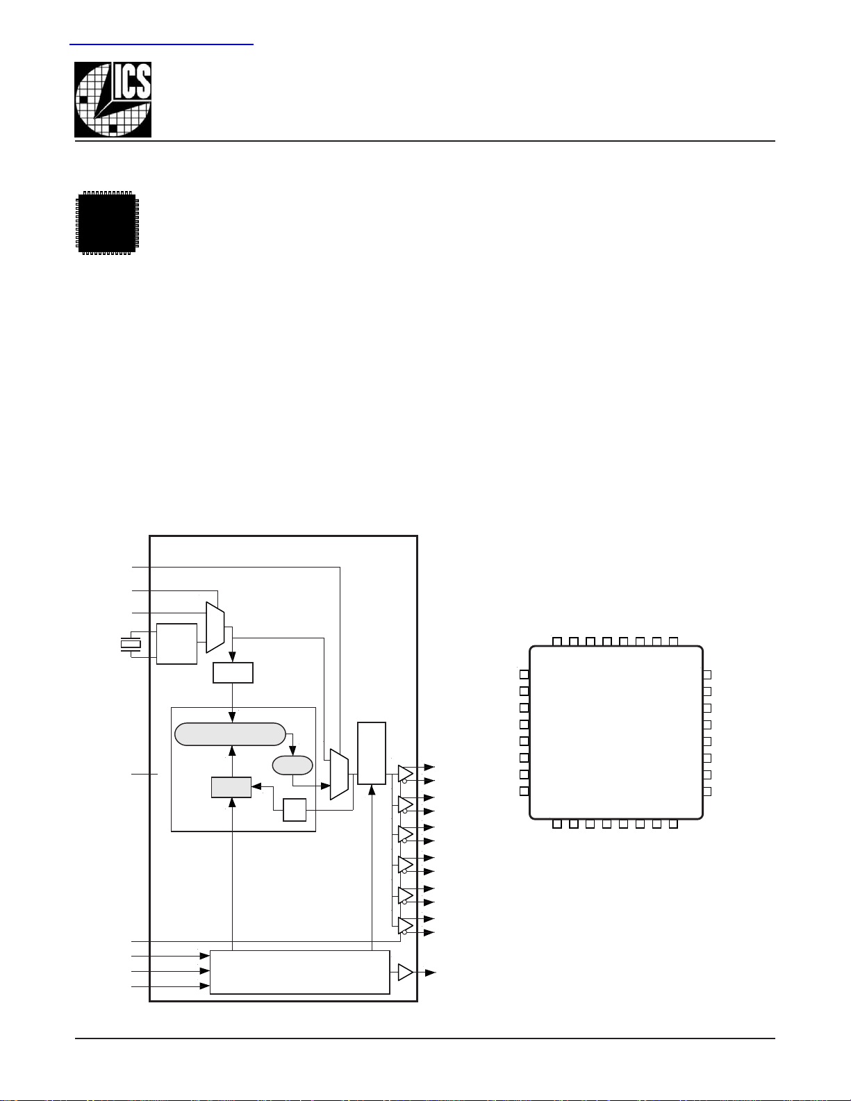
BLOCK DIAGRAM
The ICS8427-02 is a general purpose, six
LVHSTL output high frequency synthesizer
and a member of the HiPerClockS™ family of
High Performance Clock Solutions from ICS.
The ICS8427-02 can support a very wide
ICS8427-02
500MHZ, LOW JITTER
FEATURES
• Six differential LVHSTL outputs
• Selectable crystal input interface or TEST_CLK input
• TEST_CLK accepts the following input types:
LVCMOS, LVTTL
• Output frequency range: 15.625MHz to 500MHz
• VCO range: 250MHz to 500MHz
• Serial interface for programming feedback and output dividers
• Supports SSC, -0.5% downspread. Can be enabled through
use of the serial programming interface.
• Output skew: 100ps (maximum)
• Cycle-to-cycle jitter: 50ps (maximum)
• 2.5V core/1.8V output supply voltage
• 0°C to 70°C ambient operating temperature
• Industrial temperature information available upon request
• Available in both standard and lead-free RoHS-compliant
packages
VCO_SEL
XTAL_SEL
TEST_CLK
XTAL_IN
XTAL_OUT
MR
OE
S_LOAD
S_DATA
S_CLOCK
0
OSC
1
÷ 16
PHASE DETECTOR
÷ M
PLL
VCO
÷ 2
CONFIGURATION
INTERFACE
LOGIC
PIN ASSIGNMENT
VCO_SEL
V
DD
nFOUT5
FOUT5
XTAL_IN
GND
24
23
22
21
20
19
18
17
XTAL_OUT
TEST_CLK
XTAL_SEL
V
DDA
S_LOAD
S_DATA
S_CLOCK
MR
nFOUT1
32 31 30 29 28 27 26 25
V
DDO
1
FOUT2
nFOUT2
÷ 1,
÷ 2,
÷ 4,
0
÷ 8,
÷ 16
1
FOUT0
nFOUT0
FOUT1
nFOUT1
FOUT2
nFOUT2
FOUT3
nFOUT3
FOUT4
nFOUT4
FOUT5
nFOUT5
FOUT3
nFOUT3
2
3
V
DDO
4
5
6
OE
7
8
GND
9 10 11 12 13 14 15 16
7mm x 7mm x 1.4mm package body
nFOUT0
V
DDO
FOUT0
FOUT1
ICS8427-02
V
nFOUT4
FOUT4
VDDTEST
32-Lead LQFP
DDO
Y Package
Top View
32-Lead VFQFN
TEST
5mm x 5mm x 0.75mm package body
K Package
Top View
8427DY-02 www.icst.com/products/hiperclocks.html REV. A FEBRUARY 17, 2006
1
Page 2
Integrated
Circuit
Systems, Inc.
LVCMOS/CRYSTAL-TO-LVHSTL FREQUENCY SYNTHESIZER
FUNCTIONAL DESCRIPTION
NOTE: The functional description that follows describes operation using a 16.6667MHz crystal. Valid PLL loop divider
values for different crystal or input frequencies are defined in
the Input Frequency Characteristics, T ab le 6 NO TE 1.
The ICS8427-02 features a fully integrated PLL and therefore
requires no external components for setting the loop bandwidth.
A parallel-resonant, fundamental crystal is used as the input to
the on-chip oscillator. The output of the oscillator is divided by
16 prior to the phase detector. With a 16.6667MHz crystal, this
provides a 1.0417MHz reference frequency. The VCO of the
PLL operates over a range of 250MHz to 500MHz. The output of
the M divider is also applied to the phase detector.
The phase detector and the M divider force the VCO output frequency to be 2M times the reference frequency by adjusting
the VCO control voltage. Note that for some values of M (either too
high or too low), the PLL will not achieve lock. The output of the
VCO is scaled by a divider prior to being sent to each of the LVPECL
output buffers. The divider provides a 50% output duty cycle.
The ICS8427-02 powers up by default to 200MHz output frequency, using a 16.6667MHz crystal (M = 192, N = 2). The
output frequency can be changed after power-up by using the
serial interface to program the M feedback divider and the N
output divider.
ICS8427-02
500MHZ, LOW JITTER
The M value and the required values of M0 through M8 are shown
in Table 3B, Programmable VCO Frequency Function Table. Valid
M values for which the PLL will achieve lock for a 16.6667MHz
reference are defined as 120 ≤ M ≤ 240. The frequency out is
defined as follows:
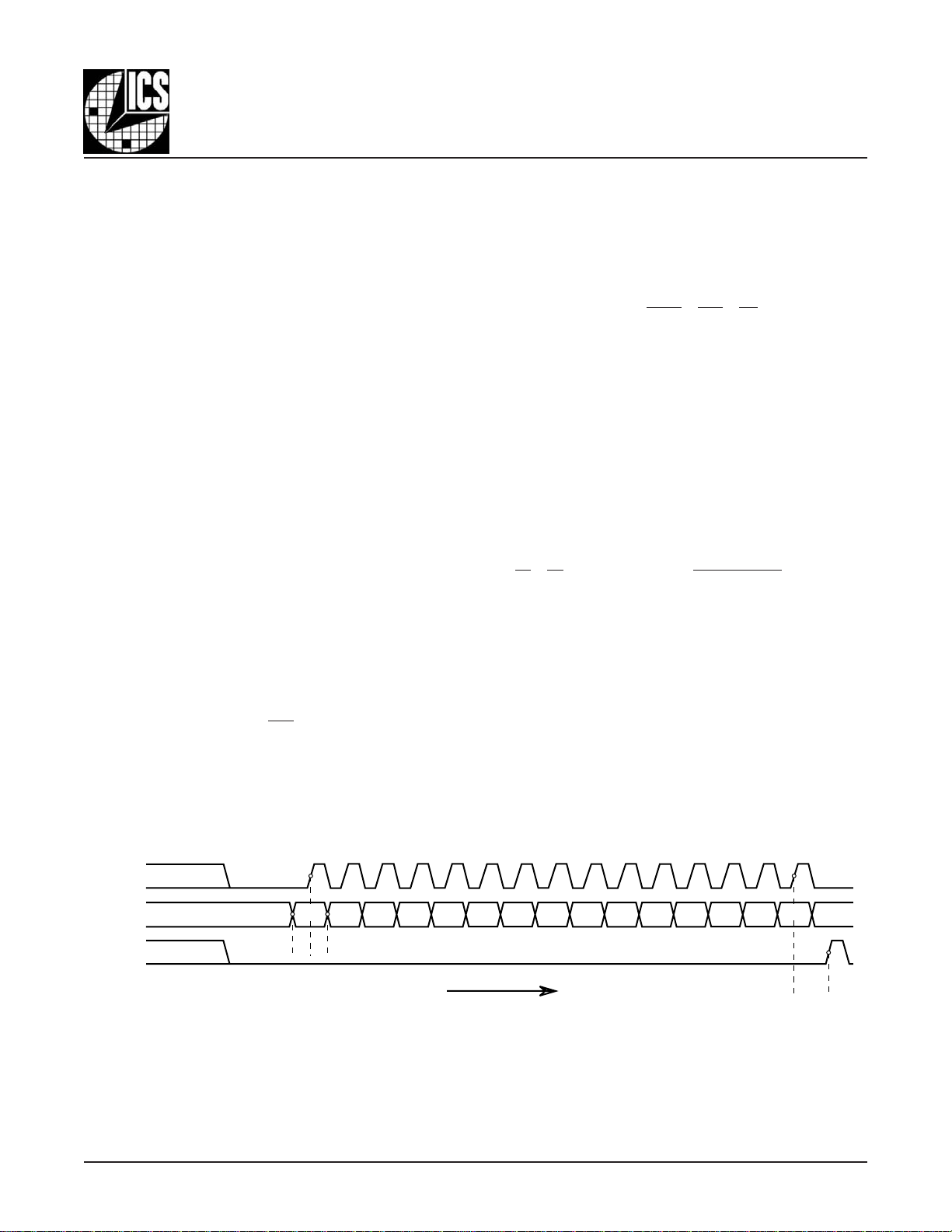
Serial operation occurs when S_LOAD is LOW. The shift
register is loaded by sampling the S_DATA bits with the rising
edge of S_CLOCK. The contents of the shift register are
loaded into the M divider and N output divider when S_LOAD
transitions from LOW-to-HIGH. The M divide and N output
divide values are latched on the HIGH-to-LOW transition of
S_LOAD. If S_LOAD is held HIGH, data at the S_DATA input
is passed directly to the M divider and N outputdivider on each
rising edge of S_CLOCK. The serial mode can be used to
program the M and N bits and test bits T1 and T0. The internal
registers T0 and T1 determine the state of the TEST output
as follows:
T1 T0 TEST Output
0 0 LOW
0 1 S_Data, Shift Register Input
1 0 Output of M divider
1 1 CMOS Fout
(Power-up
Default)
fout
=
fVCO
N
=
16
2Mfxtal
x
N
The relationship between the VCO frequency, the crystal frequency and the M divider is defined as follows:
fxtal
fVCO =
S_CLOCK
S_DATA
S_LOAD
16
x 2M
T1 T0
tSt
H
N2
N1 N0 M8 M7 M6 M5 M4 M3 M2 M1 M0 SSC
Time
FIGURE 1. SERIAL LOAD OPERATIONS
NOTE: Default Output Frequency, using a 16.6667MHz crystal
on power-up = 200MHz (M = 192, N = 2) SSC off
t
S
8427DY-02 www.icst.com/products/hiperclocks.html REV. A FEBRUARY 17, 2006
2
Page 3
Integrated
Circuit
Systems, Inc.
Test Mode
Control Register
LVCMOS/CRYSTAL-TO-LVHSTL FREQUENCY SYNTHESIZER
M AND N DIVIDERS, SSC AND TEST MODE CONTROL BITS
N Divider
M Divider
ICS8427-02
500MHZ, LOW JITTER
SSC Control
Register
➤
➤
➤
S_DATA
➤
➤
1T0T2N1N0N8M7M6M5M4M3M2M1M0MCSS
➤
1T0T2N1N0N8M7M6M5M4M3M2M1M0MCSS
➤
➤
➤
➤
➤
➤
➤
➤
➤
➤
➤
➤
➤
➤
➤
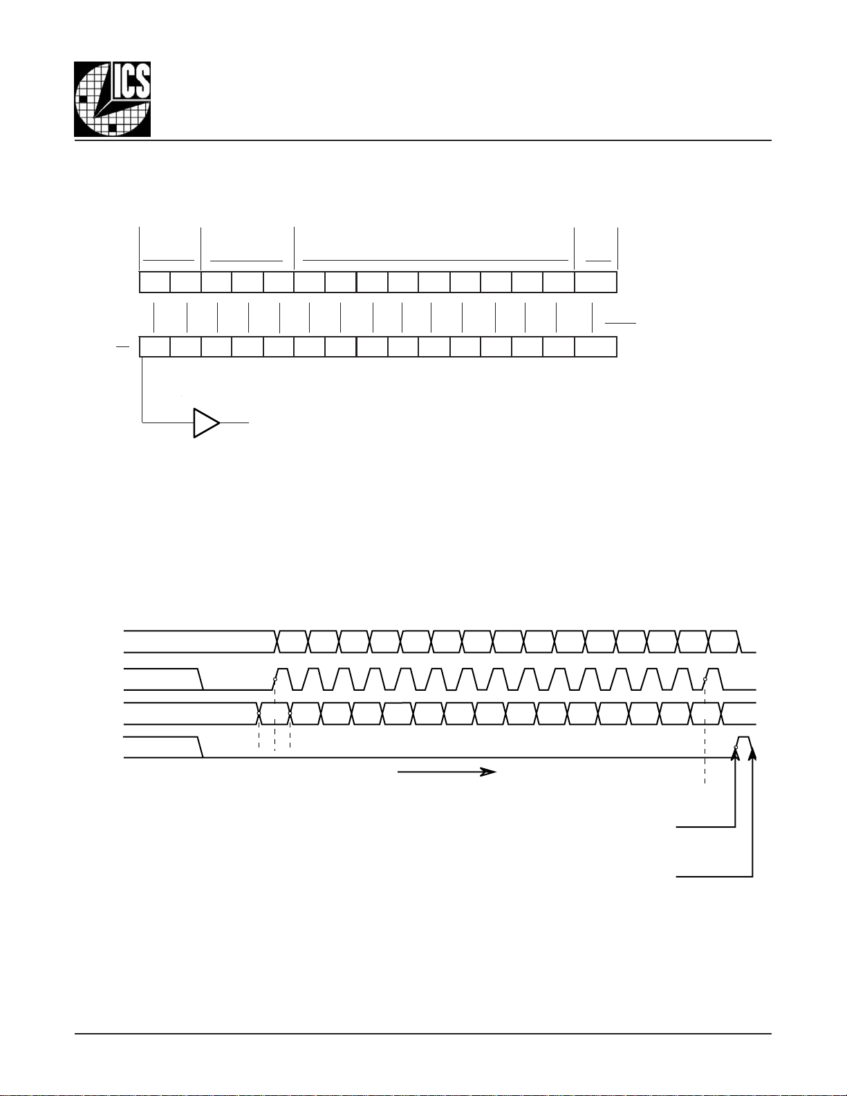
Shift Register
TEST Output
T1:T0 = 01
ICS8427-02 SHIFT REGISTER OPERATION – READ BACK CAPABILITY
1. Device powers up by default in Test Mode 01.
The Test Output in this case is wired to the shift register.
2. Shift in serial data stream and latch into M, N, T1, T0 and SSC Control Bits.
Shift in T1:T0=00, so that the TEST Output will be turned off after the bits are shifted in and latched.
TEST Output
T1 T0 N2 N1 N0 M8 M7 M6 M5 M4 M3 M2 M1 M0 SSC
➤
➤
➤
➤
Data transfer from shift register
to M and N dividers and SSC and
Test Control Bits on a low-to-high
transition of S_LOAD.
S_CLOCK
S_DATA
S_LOAD
8427DY-02 www.icst.com/products/hiperclocks.html REV. A FEBRUARY 17, 2006
T1 T0 N2 N1 N0 M8 M7 M6 M5 M4 M3 M2 M1 M0 SSC
tSt
H
Time
Data transferred to M, N dividers, TEST and SSC Control Bits.
Changes to M, N, SSC and TEST mode bits take affect at this time.
Data latched into M, N Dividers, TEST and SSC control bits.
3
t
S
Page 4

Integrated
Circuit
Systems, Inc.
LVCMOS/CRYSTAL-TO-LVHSTL FREQUENCY SYNTHESIZER
TABLE 1. PIN DESCRIPTIONS
rebmuNemaNepyTnoitpircseD
03,31,4,1V
3,2
6,5
7EOtupnIpulluP
61,8DNGrewoP.dnuorgylppusrewoP
9TSETtupt
62,01V
21,11
51,41
71RMtupnInwodlluP
81KCOLC_StupnIpulluP
91ATAD_StupnIpulluP
02DAOL_StupnInwodlluP
12V
22
32KLC_TSETtupnInwodlluP.slevelec
52,42
72LES_OCVtupnIpulluP
92,82
23,13
:ETON pulluP dna nwodlluP .seulavlacipytrof,scitsiretcarahCn
ODD
,2TUOF
2TUOFn
,3TUOF
3TUOFn
DD
,4TUOF
4TUOFn
,5TUOF
5TUOFn
ADD
LES_LATX
,TUO_LATX
NI_LATX
,0TUOF
0TUOFn
,1TUOF
1TUOFn
rewoP.snipylppustuptuO
tuptuO.slevelecafretniLTSH.riaptuptuolaitnereffiD
tu
ptuO.slevelecafretniLTSH.riaptuptuolaitnereffiD
uO
rewoP.snipylppuseroC
tuptuO.slevelecafretniLTSH.riaptuptuolaitnereffiD
tuptuO.slevelecafretniLTSH.riaptuptuolaitnereffiD
rewoP.nipylppusgolanA
tupnIpulluP
tupnI
tuptuO.slevelecafretniLTSH.riaptuptuolaitnereffiD
tup
tuO.slevelecafretniLTSH.riaptuptuolaitnereffiD
giHevitcA
retsaMhgiHevitcA
syrC
.tuptuoehtsiTUO_LATX
etniLTTVL/SOMCVL
iP,2elbaTeeS.srotsisertupnilanretniotrefer
ICS8427-02
500MHZ, LOW JITTER
.delbaneerastuptuoeht,HGIHnehW.elbanetuptuoh
.hgiH=xTUOFn,woL=xTUOF,WOLnehW
.slevelecafretniLTTVL/SOMCVL
.noitarepofoedomlairesehtniEVITCAsihcihwtuptuotseT
.slevelecafretniLTTVL/SOMCVL
sredividlanretnieht,HGIHcigolnehW.teseR
detrevniehtdnawologotxTUOFstuptuoeurtehtgnisuacteserera
hW.hgihogotxTUOFnstuptuo
.retsige
rtfihsehtotniATAD_SlairesdaolotkcolctupnI
.slevelecafretniLTTVL/SOMCVL
odelpmasataD.tupnilairesretsigertfihS
.slevelecafretniLTTVL/SOMCVL.KCOLC_S
htotniretsigertfihsmorfatadfonoitisnartslortnoC
.slevelecafretniLTTVL/SOMCVL
celeS.HGIHnehwtupniLATXstceleS.ecruos
.slevelecafretniLTTVL/SOMCVL.WOLnehw
afretniLTTVL/SOMCVL.tupnikcolctseT
.tupniehtsiNI_LATX.ecafretnirotallicsolat
.slevelecafr
sredividlanretnieht,WOLcigolne
.slevelecafretniLTTVL/SOMCVL.delbaneerastuptuoehtdna
foegdegnisirehtn
.sredivide
ecnereferLLPehtsatupnitsetrotupniLATXneewtebstceleS
KLC_TSETst
.edomssapybroLLPnisirezisehtnysrehtehwsenimreteD
TABLE 2. PIN CHARACTERISTICS
lobmySretemaraPsnoitidnoCtseTmuminiMlacipyTmumixaMstinU
C
NI
R
PULLUP
R
8427DY-02 www.icst.com/products/hiperclocks.html REV. A FEBRUARY 17, 2006
NWODLLUP
ecnaticapaCtupnI 4Fp
rotsiseRpulluPtupnI 15kΩ
rotsiseRnwodlluPtupnI 15kΩ
4
Page 5
Integrated
Circuit
Systems, Inc.
LVCMOS/CRYSTAL-TO-LVHSTL FREQUENCY SYNTHESIZER
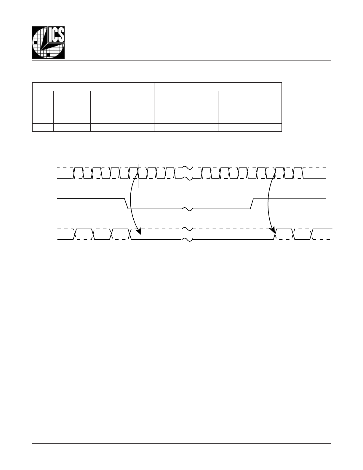
TABLE 3A. CONTROL INPUT FUNCTION TABLE
stupnIstuptuO
EOLES_LATXecruoSdetceleS5TUOF:0TUOF5TUOFn:0TUOFn
00 KLC_TSETWOL;delbasiDHGIH;delbasiD
01 TUO_LATX,NI_LA
10 KLC_TSETdelbanEdelbanE
11 TUO_LATX,NI_LATXdelbanEdelbanE
ninwohssa .2erugiF
TXWOL;delbasiDHGIH;delbasiD
ollofdelbanerodelbasiderastuptuokcolceht,sehctiwsEOretfA
ICS8427-02
500MHZ, LOW JITTER
egdeOCVgnillafdnagnisiragniw
nVCO
VCO
OE
nFOUT0:5
FOUT0:5
Disabled
FIGURE 2. OE TIMING DIAGRAM
Enabled
8427DY-02 www.icst.com/products/hiperclocks.html REV. A FEBRUARY 17, 2006
5
Page 6
Integrated
Circuit
Systems, Inc.
ICS8427-02
500MHZ, LOW JITTER
LVCMOS/CRYSTAL-TO-LVHSTL FREQUENCY SYNTHESIZER
TABLE 3B. PROGRAMMABLE VCO FREQUENCY FUNCTION T ABLE
ycneuqerFOCV
)zHM(
052021 00 1111000
80.252121 001111001
71.452221 00 11110 10
• • •••••••••
004291 0 11000000
• • •••••••••
29.794932 01110 1111
005042 011110000
ediviDM
6528214623618421
8M7M6M5M4M3M2M1M0M
NOTE 1
TABLE 3C. SERIAL MODE FUNCTION TABLE
stupnI
RMDAOL_SKCOLC_SATAD_S
HX X X .hgiH=xTUOFn,woL=xTUOF.WOLlaitnereffidstuptuosecroF.teseR
LL X X
LL
L
L
LL X X .sretsigertf
LH
↑
↓
↑ noitisnartegdegnisiR=
↓ noitisnartegdegnillaF=
↑
LataD .redividtuptuoNdnaredivi
LataD.dehctaleraseulavredividtuptuoNdnaredividM
↑
WOL=L:ETON
HGIH=H
eract'noD=X
ataD
ataD.dekcolcsitisaredividMotyltceriddessapATAD_S
snoitidnoC
.KCOLC_Sfoegde
qerftupninaotdnopserrocseicneuqerfgnitluserehtdnaseulavedividMesehT:1ETON
.sruccotnevelairesalitnuro
dMehtotdessaperaretsigertfihsehtfostnetnoC
ihstceffatonodtupnilaireS
.zHM7666.61foycneu
noitisna
rtWOLtxenlitnudedaolsniamerdnasretsigertupniotnidehctalsiataD
aenoATAD_SnoatadhtiwdedaolsiretsigertfihS.edomtupnilaireS
gnisirhc
TABLE 3D. PROGRAMMABLE OUTPUT DIVIDER FUNCTION TABLE
tupnI
2N1N0NmuminiMmumixaM
000 2 521052
00 1 4 5.26521
010 8 52.135.26
011 61526.5152.13
10 0 1 052005
10 1 2 521052
110 4 5.26521
111 8 5
8427DY-02 www.icst.com/products/hiperclocks.html REV. A FEBRUARY 17, 2006
eulaVrediviDN
2.135.26
6
)zHM(ycneuqerFtuptuO
Page 7
Integrated
Circuit
Systems, Inc.
ABSOLUTE MAXIMUM RATINGS
ICS8427-02
500MHZ, LOW JITTER
LVCMOS/CRYSTAL-TO-LVHSTL FREQUENCY SYNTHESIZER
Supply Voltage, V
Inputs, V
I
Outputs, I
Continuous Current 50mA
DD
O
4.6V
-0.5V to V
DD
Surge Current 100mA
Package Thermal Impedance, θ
JA
for 32 Lead LQFP 47.9°C/W (0 lfpm)
for 32 Lead VFQFN 34.8°C/W (0 lfpm)
Storage Temperature, T
STG
-65°C to 150°C
TABLE 4A. POWER SUPPLY DC CHARACTERISTICS, V
lobmySretemaraPsnoitidnoCtseTmuminiMlacipyTmumixaMstinU
V
DD
V
ADD
V
ODD
I
DD
I
ADD
I
0DD
ylppuSeroC573.25.2526.2V
egatloVgolanA573.25.2526.2V
egatloVtuptuO6.18.10.2V
tnerruCylppuSrewoP 571Am
tnerruCylppuSgolanA 51Am
tnerruCylppuStuptuOdaoLoN0Am
+ 0.5V
= V
DD
NOTE: Stresses beyond those listed under Absolute
Maximum Ratings may cause permanent damage to the
device. These ratings are stress specifications only. Functional
operation of product at these conditions or any conditions be-
yond those listed in the DC Characteristics or AC Character-
istics is not implied. Exposure to absolute maximum rating
conditions for extended periods may affect product reliability.
= 2.5V±5%, V
DDA
= 1.8V±0.2V, TA = 0°C TO 70°C
DDO
TABLE 4B. LVCMOS/LVTTL DC CHARACTERISTICS, V
lobmySretemaraPsnoitidnoCtseTmuminiMlacipyTmumixaMstinU
V
HI
V
LI
I
HI
I
LI
V
HO
V
LO
tupnI
tupnI
tuptuO
tuptuO
egatloVhgiHtupnI 7.1V
egatloVwoLtupnI 3.0-7.0V
KLC_TSET,DAOL_S,RMV
tnerruChgiH
,LES_OCV,LES_LATX
EO,ATAD_S,KCOLC_S
KLC_TSET,DAOL_S,RM
tnerruCwoL
,LES_OCV,LES_LATX
EO,ATAD_S,KCOLC_S
egatloVhgiH
egatloVwoL
1ETON;TSET5.1V
1ETON;TSET 4.0V
05htiwdetanimretstuptuO:1ETON Ω Vot
.2/
ODD
DD
= V
DDA
V
= 2.5V±5%, V
V=
DD
NI
V=
DD
NI
=V526.2,
V
DD
V
V0=
NI
=,V526.2
V
DD
V0=
V
NI
= 1.8V±0.2V, TA = 0°C TO 70°C
DDO
3.0+V
DD
V526.2=051Aµ
V526.2=5Aµ
5-Aµ
051-Aµ
8427DY-02 www.icst.com/products/hiperclocks.html REV. A FEBRUARY 17, 2006
7
Page 8
Integrated
Circuit
Systems, Inc.
ICS8427-02
500MHZ, LOW JITTER
LVCMOS/CRYSTAL-TO-LVHSTL FREQUENCY SYNTHESIZER
TABLE 4C. LVHSTL DC CHARACTERISTICS, V
lobmySretemaraPsnoitidnoCtseTmuminiMlacipyTmumixaMstinU
V
HO
V
LO
V
XO
V
GNIWS
1ETON;egatloVhgiHtuptuO9.03.1V
1ETON;egatloVwoLtuptuO04.0V
05htiwdetanimretstuptuO:1ETON Ω V5.2eeS.DNGot erugiftiucriCtseTdaoLtup
eD:2ETON
TABLE 5. CRYSTAL CHARACTERISTICS
retemaraPsnoitidnoCtseTmuminiMlacipyTmumixaMstinU
noitallicsOfoedoM latnemadnuF
ycneuqerF 2104zHM
seireStnelaviuqE 05
ecnaticapaCtnuhS 7Fp
leveLevirD 1Wm
TABLE 6. INPUT CHARACTERISTICS, V
)RSE(ecnatsiseR
= V
DD
= 2.5V±5%, V
DDA
= V
DD
= 2.5V±5%, V
DDA
= 1.8V±0.2V, TA = 0°C TO 70°C
DDO
2ETON;egatloVrevossorCtuptuO0406%
gniwSegatloVtuptuOkaeP-ot-kaeP6.01.1V
tuO ehtni
.noitcesnoitamrofnItnemerusaeMretemaraP
.noitidnocnevigatagniwsegatlovtuptuoottcepserhtiwdenif
Ω
= 1.8V±0.2V, TA = 0°C TO 70°C
DDO
lobmySretemaraPsnoitidnoCtseTmuminiMlacipyTmumixaMstinU
1=tcelesOCV2104zHM
KLC_TSET
)edomssapyb(0=tcelesOCV004zHM
f
NI
ycneuqerFtupnI
1ETON;LATX2104zHM
KCOLC_S 05zHM
t
TUPNI_r
emiTesiRtupnIKLC_TSET 5sn
ehtroF:1ETON
761eraMfoseulavdilavzHM21foycneuqerfmuminimehtgnisU.zHM005rozHM052foegnar ≤ M ≤ 652 . ehtgnisU
5eraMfoseulavdilavzHM04foycneuqerfmumixam ≤ M ≤ .001
0
ycneuqerfOCVmumixamromuminimehteveihcaottesebtsumeulavMehtegnarycneuqerflatsyrc
8427DY-02 www.icst.com/products/hiperclocks.html REV. A FEBRUARY 17, 2006
8
Page 9

Integrated
Circuit
Systems, Inc.
ICS8427-02
500MHZ, LOW JITTER
LVCMOS/CRYSTAL-TO-LVHSTL FREQUENCY SYNTHESIZER
TABLE 7. AC CHARACTERISTICS, V
DD
= V
DDA
= 2.5V±5%, V
= 1.8V±0.2V, TA = 0°C TO 70°C
DDO
lobmySretemaraPsnoitidnoCtseTmuminiMlacipyTmumixaMstinU
F
XAM
t )cc(tij3,1ETON;rettiJelcyC-ot-elcyC
t )05T(ttijrettiJelcyC05T
ycneuqerFtuptuO 005zHM
F
TUO
F
TUO
F
TUO
F
TUO
F
TUO
F
TUO
F
TUO
F
TUO
zHM002=0305sp
zHM762=0305sp
zHM333=0305sp
zHM004=0305sp
zHM002=002sp
zHM762=002sp
zHM333=002sp
zHM004=002sp
t )rep(tij1ETON;SMR,rettiJdoireP 5.25sp
t )o(ks3,2ETON;wekStuptuO 56001sp
F
M
F
FM
CSS
feR
rups
t
Rt/F
t
S
t
H
cdoelcyCytuDtuptuO
t
KCOL
F
TUO
F
5,4ETON;ycneuqerFnoitaludoMCSS
5,4ETON;rotcaFnoitaludoMCSS
der
5,4ETON;noitcudeRlartcepS
rupSecnerefeR
TUO
F
TUO
F
TUO
F
TUO
F
TUO
F
TUO
F
TUO
F
TUO
F
TUO
F
TUO
F
TUO
F
TUO
F
TUO
F
TUO
F
TUO
emiTllaF/esiRtuptuO%08ot%02333766sp
emiTputeS
emiTdloH
KCOLC_SotATAD_S5sn
DAOL_SotKCOLC_S5sn
KCOLC_SotATAD_S5sn
DAOL_SotKCOLC_S5sn
emiTkcoLLLP 1sm
zHM002=0333.33zHk
zHM762=0333.33zHk
zHM333=0333.33zHk
zHM004=0333.33zHk
zHM002=3.06.0%
zHM762=4.06.0%
zHM333=3.06.0%
zHM004=3.06.0%
zHM002=7-01-Bd
zHM762=7-21-Bd
zHM333=7-11-Bd
zHM004=7-21-Bd
zHM002=04-Bd
zHM762=04-Bd
zHM333=54-Bd
zHM004=05-Bd
1=N0406%
2=N5455%
.noitcesnoitamrofnItnemerusaeMretemaraPeeS
.stupniLATXgnisuecnamrofreprettiJ:1ETON
.snoiti
dnocdaollauqehtiwdnaegatlovylppusemasehttastuptuoneewtebwekssadenifeD:2ETON
ptuoehttaderusaeM
.stniopssorclaitnereffidtu
.56dradnatSCEDEJhtiwecnadroccanidenifedsiretemarapsihT:3ETON
daerpS:4ETON
.delbanegnikcolcmurtcepS
.latsyrcztrauqzHM7666.61agnisU:5ETON
8427DY-02 www.icst.com/products/hiperclocks.html REV. A FEBRUARY 17, 2006
9
Page 10

2.5V±5%
t
➤
t
r
V
DDA
Integrated
Circuit
Systems, Inc.
= 2.5V±5%
1.8V±0.2V
ICS8427-02
500MHZ, LOW JITTER
LVCMOS/CRYSTAL-TO-LVHSTL FREQUENCY SYNTHESIZER
PARAMETER MEASUREMENT INFORMATION
nFOUTx
V
DD
V
DDO
Qx
LVHSTL
GND
0V
nQx
2.5V CORE/1.8V OUTPUT LOAD AC TEST CIRCUIT
nFOUT0:5
FOUT0:5
➤
tcycle n tcycle n+1
➤
➤
tjit(cc) = tcycle n –tcycle n+1
1000 Cycles
SCOPE
FOUTx
nFOUTy
FOUTy
OUTPUT SKEW
nFOUT0:5
FOUT0:5
jit (50) = Period n – Period n +50
Minimum 16,667 consective cycles
334 measurements
sk(o)
Period n
Period n + 50
Period n
+ 50 + 50
CYCLE-TO-CYCLE JITTER
Reference Spu
dBm
Frequency
SPUR REDUCTION
8427DY-02 www.icst.com/products/hiperclocks.html REV. A FEBRUARY 17, 2006
T50 CYCLE-TO-CYCLE JITTER
1σ contains 68.26% of all measurements
2σ contains 95.4% of all measurements
3σ contains 99.73% of all measurements
4σ contains 99.99366% of all measurements
6σ contains (100-1.973x10
Reference Point
(Trigger Edge)
-7
PERIOD JITTER
10
)% of all measurements
Histogram
Mean Period
(First edge after trigger)
V
OH
V
REF
V
OL
Page 11

Integrated
Circuit
Systems, Inc.
ICS8427-02
500MHZ, LOW JITTER
LVCMOS/CRYSTAL-TO-LVHSTL FREQUENCY SYNTHESIZER
nFOUT0:5
V
OX
FOUT0:5
OUTPUT CROSSOVER VOLTAGE
Clock
Outputs
20%
80%
t
R
80%
t
F
20%
V
SWI NG
V
60%
50%
40%
V
OH
OL
nFOUT0:5
FOUT0:5
tPW
odc = x 100%
OUTPUT DUTY CYCLE/PULSE WIDTH/PERIOD
t
PERIOD
t
t
PERIOD
PW
OUTPUT RISE/FALL TIME
8427DY-02 www.icst.com/products/hiperclocks.html REV. A FEBRUARY 17, 2006
11
Page 12

Integrated
X1
C2
Circuit
Systems, Inc.
LVCMOS/CRYSTAL-TO-LVHSTL FREQUENCY SYNTHESIZER
APPLICATION INFORMATION
RECOMMENDATIONS FOR UNUSED INPUT AND OUTPUT PINS
ICS8427-02
500MHZ, LOW JITTER
INPUTS:
CRYSTAL I NPUT:
For applications not requiring the use of the crystal oscillator
input, both XTAL_IN and XTAL_OUT can be left floating.
Though not required, but for additional protection, a 1kΩ
resistor can be tied from XTAL_IN to ground.
TEST_CLK I
For applications not requiring the use of the test clock, it can
be left floating. Though not required, but for additional
protection, a 1kΩ resistor can be tied from the TEST_CLK to
ground.
LVCMOS C
All control pins have internal pull-ups or pull-downs; additional
resistance is not required but can be added for additional
protection. A 1kΩ resistor can be used.
NPUT:
ONTROL PINS:
CRYSTAL INPUT INTERFACE
The ICS8427-02 has been characterized with 18pF parallel
resonant crystals. The capacitor values, C1 and C2, shown in
Figure 3 below were determined using a 16.66MHz, 18pF
OUTPUTS:
LVHSTL OUTPUT
All unused LVHSTL outputs can be left floating. We recommend
that there is no trace attached. Both sides of the differential
output pair should either be left floating or terminated.
parallel resonant crystal and were chosen to minimize the
ppm error. The optimum C1 and C2 values can be slightly
adjusted for different board layouts.
XTAL_OUT
C1
22p
18pF Parallel Crystal
XTAL_IN
22p
Figure 3. CRYSTA L INPUt INTERFACE
8427DY-02 www.icst.com/products/hiperclocks.html REV. A FEBRUARY 17, 2006
12
Page 13

Integrated
➤
➤
Circuit
Systems, Inc.
LVCMOS/CRYSTAL-TO-LVHSTL FREQUENCY SYNTHESIZER
POWER SUPPLY FILTERING T ECHNIQUES
As in any high speed analog circuitry, the power supply pins
are vulnerable to random noise. The ICS8427-02 provides
separate power supplies to isolate any high switching
, V
noise from the outputs to the internal PLL. V
should be individually connected to the power supply
plane through vias, and bypass capacitors should be
used for each pin. To achieve optimum jitter performance,
power supply isolation is required. Figure 4 illustrates how
a 10Ω resistor along with a 10μF and a .01μF bypass
capacitor should be connected to each V
DDA
SPREAD SPECTRUM
Spread-spectrum clocking is a frequency modulation technique for EMI reduction. When spread-spectrum is enabled, a
32.55kHz triangle waveform is used with 0.5% down-spread
(+0.0% / -0.5%) from the nominal 200MHz clock frequency.
An example of a triangle frequency modulation profile is shown
in Figure 5A below. The ramp profile can be expressed as:
• Fnom = Nominal Clock Frequency in Spread OFF mode
(200MHz with 16.6667MHz IN)
• Fm = Nominal Modulation Frequency
= Reference Frequency
16 x 32
• δ = Modulation Factor (0.5% down spread)
DD
pin.
DDA
, and V
DDO
ICS8427-02
500MHZ, LOW JITTER
2.5V
V
DD
.01μF
V
DDA
.01μF
FIGURE 4. POWER S UPPLY FILTERING
The ICS8427-02 triangle modulation frequency deviation will
not exceed 0.6% down-spread from the nominal clock frequency (+0.0% / -0.5%). An example of the amount of down
spread relative to the nominal clock frequency can be seen in
the frequency domain, as shown in Figure 5B. The ratio of this
width to the fundamental frequency is typically 0.4%, and will
not exceed 0.6%. The resulting spectral reduction will be
greater than 7dB, as shown in Figure 5B. It is important to
note the ICS8427-02 7dB minimum spectral reduction is the
component-specific EMI reduction, and will not necessarily
be the same as the system EMI reduction.
10Ω
10μF
(1 - δ) fnom + 2 fm x δ x fnom x t when 0 < t < ,
(1 - δ) fnom - 2 fm x δ x fnom x t when < t <
Fnom
(1 - δ) Fnom
0.5/fm 1/fm
1
2 fm
FIGURE 5A. TRIANGLE FREQUENCY MODULATION
8427DY-02 www.icst.com/products/hiperclocks.html REV. A FEBRUARY 17, 2006
1
2 fm
fm
1
Δ − 10 dBm
B
➤
δ = 0.3%
A
➤
FIGURE 5B. 200MHZ CLOCK OUTPUT IN FREQUENCY DOMAIN
(A) SPREAD-SPECTRUM OFF
(B) SPREAD-SPECTRUM ON
13
Page 14
Integrated
Circuit
Systems, Inc.
LVCMOS/CRYSTAL-TO-LVHSTL FREQUENCY SYNTHESIZER
LAYOUT GUIDELINE
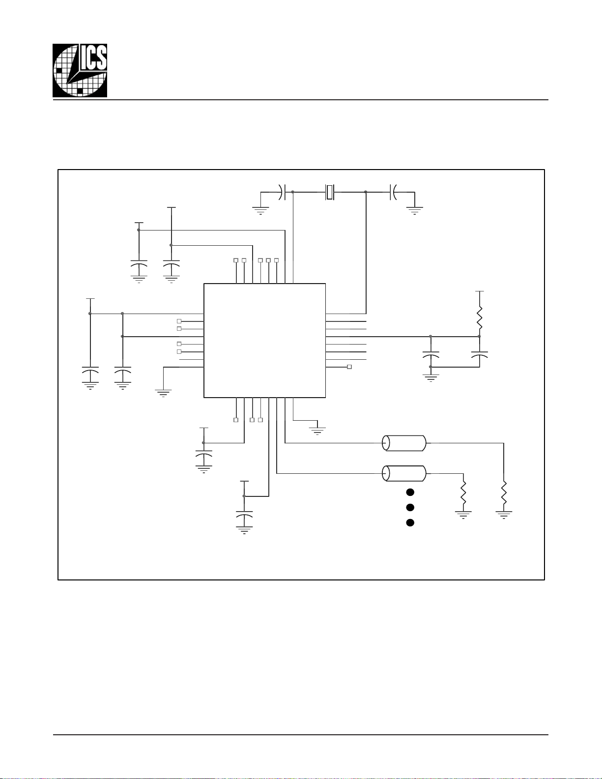
Figure 6 shows an application schematic example of the
ICS8427-02. In this example, a 16.6667MHz, 18 pF parallel
resonant crystal is used. The C1=22pF and C2=22pF are
ICS8427-02
500MHZ, LOW JITTER
approximate values for frequency accuracy. The C1 and C2
may be slightly adjusted for optimizing frequency accuracy.
VDDO = 1.8V
C7
0.1u
VDD = 2.5V
C10
0.1u
C9
0.1uF
VDDO = 1.8V
VDD = 2.5V
C8
0.1u
U1
1
2
3
4
5
6
7
8
IC S8427-02
C5
0.1u
32313029282726
VDDO
FOUT2
nFOUT2
VDDO
FOUT3
nFOUT3
OE
GND
nFOUT 1
TEST
9101112131415
VDDO = 1.8V
FOUT1
VDD
VDD O
FOUT4
C6
0.1u
nFOUT 0
nFOUT4
C1
22p
FOUT0
VDDO
VCO_SEL
FOUT5
25
VDD
XTAL1
TEST CLK
XTA L_ SE L
S_LOAD
S_DATA
S_CLOCK
nFOUT5
GND
16
X1
16.6667MHz, 18pF
MR
24
23
22
21
20
19
18
17
TEST CLK
XTAL_SEL
S_LOAD
S_DATA
S_CLOC K
XTA L2
VDD A
C2
22p
Zo = 50
Zo = 50
C3
0.01u
VDD = 2.5V
R1
10
C4
10u
R2
50
R3
50
FIGURE 6. SCHEMATIC OF RECOMMENDED LAYOUT
8427DY-02 www.icst.com/products/hiperclocks.html REV. A FEBRUARY 17, 2006
14
Page 15

Integrated
Circuit
Systems, Inc.
ICS8427-02
500MHZ, LOW JITTER
LVCMOS/CRYSTAL-TO-LVHSTL FREQUENCY SYNTHESIZER
POWER CONSIDERATIONS
This section provides information on power dissipation and junction temperature for the ICS8427-02.
Equations and example calculations are also provided.
1. P ower Dissipation.
The total power dissipation for the ICS8427-02 is the sum of the core power plus the power dissipated in the load(s).
The following is the power dissipation for V
NOTE: Please refer to Section 3 for details on calculating power dissipated in the load.
= 2.5V + 5% = 2.625V, which gives worst case results.
DD
• Power (core)
• Power (outputs)
If all outputs are loaded, the total power is 6 * 32.6mW = 195.6mW
Total Power
2. Junction Temperature.
Junction temperature, Tj, is the temperature at the junction of the bond wire and bond pad and directly affects the reliability of the
device. The maximum recommended junction temperature for HiPerClockS
Pd_total = Total Device Power Dissipation (example calculation is in section 1 above)
In order to calculate junction temperature, the appropriate junction-to-ambient thermal resistance θ
moderate air flow of 200 linear feet per minute and a multi-layer board, the appropriate value is 42.1°C/W per Table 8A below.
Therefore, Tj for an ambient temperature of 70°C with all outputs switching is:
70°C + 0.655W * 42.1°C/W = 97.6°C. This is well below the limit of 125°C.
This calculation is only an example. Tj will obviously vary depending on the number of loaded outputs, supply voltage, air flow,
and the type of board (single layer or multi-layer).
_MAX
The equation for Tj is as follows: Tj = θ
MAX
= V
MAX
* I
DD_MAX
= 32.6mW/Loaded Output pair
= 2.625V * 175mA = 459.4mW
DD_MAX
(3.465V, with all outputs switching) = 459.37mW + 195.6mW = 655mW
TM
devices is 125°C.
* Pd_total + T
JA
Tj = Junction Temperature
θ
= Junction-to-Ambient Thermal Resistance
JA
= Ambient Temperature
T
A
A
must be used. Assuming a
JA
TABLE 8A. THERMAL RESISTANCE
θθ
θJA FOR 32-PIN LQFP, FORCED CONVECTION
θθ
θθ
θJA by Velocity (Linear Feet per Minute)
θθ
0 200 500
Single-Layer PCB, JEDEC Standard Test Boards 67.8°C/W 55.9°C/W 50.1°C/W
Multi-Layer PCB, JEDEC Standard Test Boards 47.9°C/W 42.1°C/W 39.4°C/W
NOTE: Most modern PCB designs use multi-layered boards. The data in the second row pertains to most designs.
TABLE 8B. θ
VS. AIR FLOW TABLE FOR A 32 LEAD VFQFN
JA
θθ
θJA by Velocity (Linear Feet per Minute)
θθ
0
Multi-Layer PCB, JEDEC Standard Test Boards 34.8°C/W
8427DY-02 www.icst.com/products/hiperclocks.html REV. A FEBRUARY 17, 2006
15
Page 16

Integrated
Circuit
Systems, Inc.
LVCMOS/CRYSTAL-TO-LVHSTL FREQUENCY SYNTHESIZER
3. Calculations and Equations.
The purpose of this section is to derive the power dissipated into the load.
LVHSTL output driver circuit and termination are shown in Figure 7.
V
DDO
Q1
ICS8427-02
500MHZ, LOW JITTER
V
OUT
RL
50Ω
FIGURE 7. LVHSTL DRIVER CIRCUIT AND TERMINATION
To calculate worst case power dissipation into the load, use the following equations which assume a 50Ω load.
Pd_H is power dissipation when the output drives high.
Pd_L is the power dissipation when the output drives low.
Pd_H = (V
Pd_L = (V
Pd_H = (0.9V/50Ω) * (2V - 0.9V) = 19.8mW
Pd_L = (0.4V/50Ω) * (2V - 0.4V) = 12.8mW
Total Power Dissipation per output pair = Pd_H + Pd_L = 32.6mW
OH_MIN /RL
OL_MAX /RL
) * (V
) * (V
DD_MAX
DD_MAX
- V
- V
OH_MIN
OL_MAX
)
)
8427DY-02 www.icst.com/products/hiperclocks.html REV. A FEBRUARY 17, 2006
16
Page 17

Integrated
Circuit
Systems, Inc.
ICS8427-02
500MHZ, LOW JITTER
LVCMOS/CRYSTAL-TO-LVHSTL FREQUENCY SYNTHESIZER
RELIABILITY INFORMATION
TABLE 9A. θ
TABLE 9B. θ
TRANSISTOR COUNT
The transistor count for ICS8427-02 is: 4585
VS. AIR FLOW TABLE FOR 32 LEAD LQFP
JA
θθ
θJA by Velocity (Linear Feet per Minute)
θθ
Single-Layer PCB, JEDEC Standard Test Boards 67.8°C/W 55.9°C/W 50.1°C/W
Multi-Layer PCB, JEDEC Standard Test Boards 47.9°C/W 42.1°C/W 39.4°C/W
NOTE: Most modern PCB designs use multi-layered boards. The data in the second row pertains to most designs.
VS. AIR FLOW TABLE FOR A 32 LEAD VFQFN
JA
θθ
θJA 0 Air Flow (Linear Feet per Minute)
θθ
Multi-Layer PCB, JEDEC Standard Test Boards 34.8°C/W
0 200 500
0
8427DY-02 www.icst.com/products/hiperclocks.html REV. A FEBRUARY 17, 2006
17
Page 18

Integrated
Circuit
Systems, Inc.
LVCMOS/CRYSTAL-TO-LVHSTL FREQUENCY SYNTHESIZER
PACKAGE OUTLINE - Y SUFFIX FOR 32 LEAD LQFP
ICS8427-02
500MHZ, LOW JITTER
TABLE 10A. PACKAGE DIMENSIONS
NOITAIRAVCEDEJ
LOBMYS
N
A
1A
2A
b
c
D
1D
2D
E
1E
2E
e
L
q
ccc
Reference Document: JEDEC Publication 95, MS-026
8427DY-02 www.icst.com/products/hiperclocks.html REV. A FEBRUARY 17, 2006
MUMINIMLANIMONMUMIXAM
50.051.0
53.104.154.1
073.054.0
03.
90.002.0
54.006.057.0
°0°7
18
SRETEMILLIMNISNOISNEMIDLLA
ABB
23
06.1
CISAB00.9
CISAB00.7
06.5
CISAB00.9
CISAB00.7
06.5
CISAB08.0
01.0
Page 19

Integrated
Circuit
Systems, Inc.
LVCMOS/CRYSTAL-TO-LVHSTL FREQUENCY SYNTHESIZER
PACKAGE OUTLINE - K SUFFIX FOR A 32 LEAD VFQFN
ICS8427-02
500MHZ, LOW JITTER
TABLE 10B. PACKAGE DIMENSIONS
NOITAIRAVCEDEJ
LOBMYS
N
A
1A
3A
b
N
D
N
E
D
2D
E
2E
e
L
Reference Document: JEDEC Publication 95, MO-220
MUMINIMLANIMONMUMIXAM
23
08.0--00.1
0--50.0
81.052.003.0
52.152.252.3
52.152.252.3
03.004.005.0
SRETEMILLIMNISNOISNEMIDLLA
2-DHHV
.feR52.0
8
8
CISAB00.5
CISAB00.5
CISAB05.0
8427DY-02 www.icst.com/products/hiperclocks.html REV. A FEBRUARY 17, 2006
19
Page 20

Integrated
Circuit
Systems, Inc.
TABLE 11. ORDERING INFORMATION
rebmuNredrO/traPgnikraMegakcaPgnigakcaPgnippihSerutarepmeT
20-YD7248SCI20-YD7248SCIPFQLdaeL23yartC°07otC°0
T20-
YD7248SCI20-YD7248SCIPFQLdaeL23leer&epat0001C°07otC°0
FL20-YD7248SCIL20YD7248SCIPFQL"eerF-daeL"daeL23yartC°07o
TFL20-YD7248SCIL20YD7248SCIPFQL"eerF-daeL"daeL23leer&epat0001C°07otC°0
20-KD7248SCI20-KD7248SCINFQFVdaeL
T20-KD7248SCI20-KD7248SCINFQFVdaeL23leer&epat0052C°07otC°0
FL20-KD7248SCIDBTNFQFV"eerF-daeL"dae
TFL20-KD7248SCIDBTNFQFV"eerF-daeL"daeL23leer&epat0052C°07otC°0
ICS8427-02
500MHZ, LOW JITTER
LVCMOS/CRYSTAL-TO-LVHSTL FREQUENCY SYNTHESIZER
tC°0
23yartC°07otC°0
L23yartC°07otC°0
fnoceerF-bPehterarebmuntrapehtotxiffus"FL"nahtiwderedroeratahtstraP:ETON
.tnailpmocSHoReradnanoitarugi
The aforementioned trademark, HiPerClockS™ is a trademark of Integrated Circuit Systems, Inc. or its subsidiaries in the United States and/or other countries.
While the information presented herein has been checked for both accuracy and reliability, Integrated Circuit Systems, Incorporated (ICS) assumes no responsibility for either its use
or for infringement of any patents or other rights of third parties, which would result from its use. No other circuits, patents, or licenses are implied. This product is intended for use
in normal commercial applications. Any other applications such as those requiring extended temperature range, high reliability, or other extraordinary environmental requirements are
not recommended without additional processing by ICS. ICS reserves the right to change any circuitry or specifications without notice. ICS does not authorize or warrant any ICS
product for use in life support devices or critical medical instruments.
8427DY-02 www.icst.com/products/hiperclocks.html REV. A FEBRUARY 17, 2006
20
Page 21

Integrated
Circuit
Systems, Inc.
ICS8427-02
500MHZ, LOW JITTER
LVCMOS/CRYSTAL-TO-LVHSTL FREQUENCY SYNTHESIZER
TEEHSYROTSIHNOISIVER
veRelbaTegaPegnahCfonoitpircseDetaD
A
11T
01
02
.margaidtiucriCtseTCAdaoLtuptuOdetadpU
kcapPFQLrofgnikrameerf-daeldedda-elbaTnoitamrofnIgniredrO
.ega
60/71/2
8427DY-02 www.icst.com/products/hiperclocks.html REV. A FEBRUARY 17, 2006
21
 Loading...