

Page 1
查询ICS8422002I-01供应商
PRELIMINARY
Integrated
Circuit
Systems, Inc.
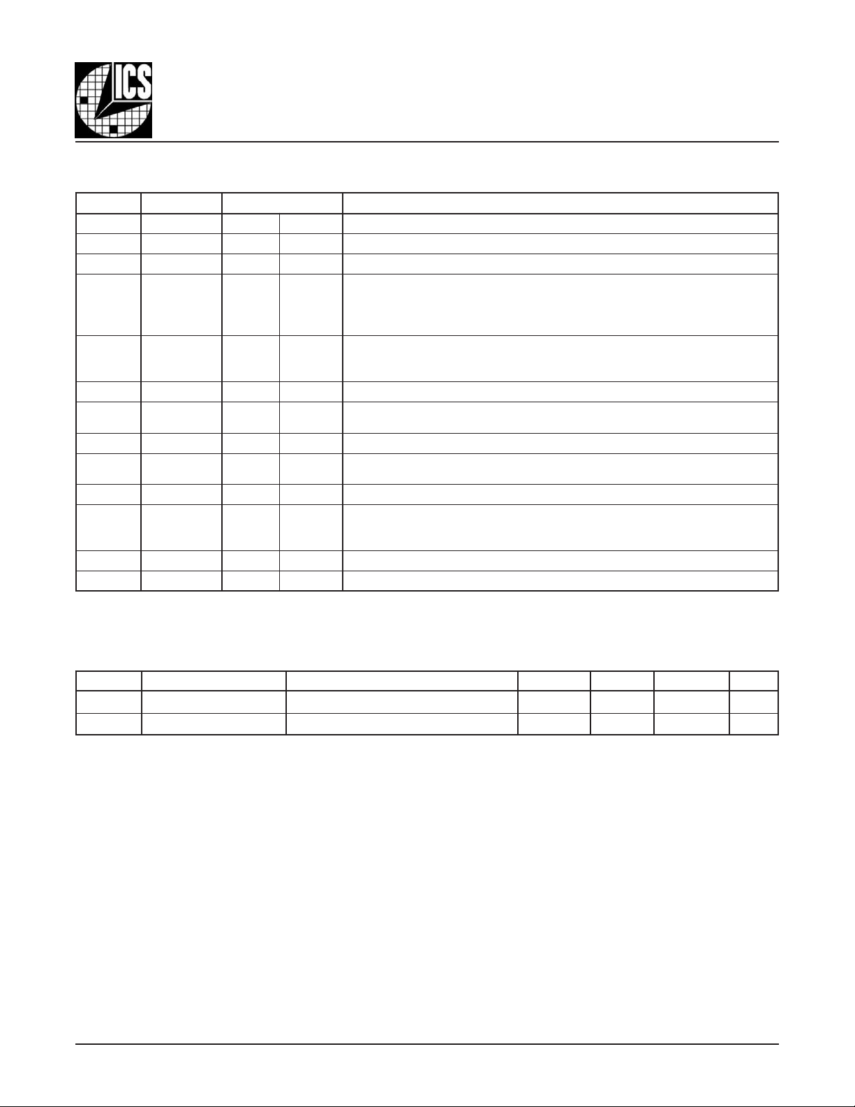
GENERAL DESCRIPTION
ICS
HiPerClockS™
parallel resonant crystal, the following frequencies can be
generated based on the 2 frequency select pins (F_SEL[1:0]):
156.25MHz, 125MHz and 62.5MHz. The ICS8422002I-01
uses ICS’ 3
and can achieve 1ps or lower typical rms phase jitter, easily
meeting Ethernet jitter requirements. The ICS8422002I-01 is
packaged in a small 20-pin TSSOP package.
The ICS8422002I-01 is a 2 output LVHSTL
Synthesizer optimized to generate Ethernet
reference clock frequencies and is a member of
TM
the HiPerClocks
family of high performance
clock solutions from ICS. Using a 25MHz 18pF
rd
generation low phase noise VCO technology
ICS8422002I-01
FEMTOCLOCKS™ C RYSTAL-TO-
LVHSTL FREQUENCY SYNTHESIZER
FEATURES
• Two LVHSTL outputs (VOHmax = 1.2V)
• Selectable crystal oscillator interface
or LVCMOS/LVTTL single-ended input
• Supports the following output frequencies: 156.25MHz,
125MHz, 62.5MHz
• VCO range: 560MHz - 680MHz
• RMS phase jitter @ 156.25MHz, using a 25MHz crystal
(1.875MHz - 20MHz): 0.44ps (typical)
• Power supply modes:
Core/Output
3.3V/1.8V
2.5V/1.8V
• -40°C to 85°C ambient operating temperature
• Available in both standard and lead-free RoHS compliant
packages
FREQUENCY SELECT FUNCTION TABLE
1LES_F0LES_F
rediviDM
eulaV
00 524 52.651
01 525 521
10 52015.26
11 desutondesuton
rediviDN
eulaV
BLOCK DIAGRAM
F_SEL[1:0]
nPLL_SEL
TEST_CLK
XTAL_IN
XTAL_OUT
nXTAL_SEL
Pulldown
Pulldown
Pulldown
25MHz
OSC
Pulldown
2
11
0
Phase
Detector
VCO
PIN ASSIGNMENT
nc
1
V
DDO
nQ0
V
V
Q0
MR
nc
DDA
DD
2
3
4
5
6
7
8
9
10
ycneuqerFtuptuO
).feRzHM52(
nPLL_SEL
F_SEL0
ICS8422002I-01
20-Lead TSSOP
6.5mm x 4.4mm x 0.92mm
package body
G Package
Top V ie w
F_SEL[1:0]
1
0
0 0 ÷4
0 1 ÷5
1 0 ÷10
1 1
Not Used
Q0
nQ0
Q1
nQ1
20
19
18
17
16
15
14
13
12
11
V
DDO
Q1
nQ1
GND
V
DD
nXTAL_SEL
TEST_CLK
XTAL_IN
XTAL_OUT
F_SEL1
M = 25 (fixed)
Pulldown
MR
The Preliminary Information presented herein represents a product in prototyping or pre-production. The noted characteristics are based on initial
product characterization. Integrated Circuit Systems, Incorporated (ICS) reserves the right to change any circuitry or specifications without notice.
8422002AGI-01 www.icst.com/products/hiperclocks.html REV. B NOVEMBER 14, 2005
1
Page 2
Integrated
Circuit
Systems, Inc.
TABLE 1. PIN DESCRIPTIONS
rebmuNemaNepyTnoitpircseD
7,1cndesunU.tcennocoN
02,2V
4,30Qn,0QtupuO.slevelecafretniLTSHVL.riaptuptuolaitnereffiD
5RMtupnInwodlluP
6LES
8V
11,9
61,01V
31,21
41KLC_TSETtupnInwodlluP.tupnikcolcLTTVL/SOMCVL
51LES_LATXntupnInwodlluP
71DNGrewoP.dnuorgylppusrewoP
91,811Q,1QntuptuO.slevelecafretniLTSHVL.riaptuptuolaitnereffiD
:ETON nwodlluP .seulavlacipytrof,scitsiretcarahCniP,2elbaTeeS.srotsisertupnilanretniotsrefer
ODD
_LLPntupnInwodlluP
ADD
,0LES_F
1LES_F
DD
,TUO_LATX
NI_LATX
rewoP.snipylppustuptuO
rewoP.nipylppusgolanA
tupnInwodlluP.slevelecafretniLTTVL/SOMCVL.sniptcelesycneuqerF
rewoP.snipylppuseroC
tupnI
PRELIMINARY
LVHSTL FREQUENCY SYNTHESIZER
teser
pniehtsiNI_LATX
.tu
retniLTTVL/SOMCVL
ICS8422002I-01
FEMTOCLOCKS™ C RYSTAL-TO-
lanretnieht,HGIHcigolnehW.teseRretsaMHGIHevitcA
erastuptuoehtdnasredividlanretnieht,WOLcigolnehW.hgihogot
.slevelecafretniLTTVL/SOMCVL.delbane
.slevelecafretniLTTVL/SOMCVL.)ssapyBLLP(
,tuptuoehtsiTUO_LATX.ecafretnilatsyrctnanoserlellaraP
pniKLC_TSETrolatsyrcneewtebstceleS
.slevelecaf
erasredivid
xQnstuptuodetrevniehtdnawologotxQstuptuoeurtehtgnisuac
nehW.sredividehtottupnisaKLC_TSETdnaLLPehtneewtebstceleS
kcolcecnereferehtstcelesed,HGIHnehW.)elbanELLP(LLPstceles,WOL
ecnerefeRLLPehtehtsastu
.HGIHnehwKLC_TSETstceleS.WOLnehwstupniLATXstceleS.ecruos
TABLE 2. PIN CHARACTERISTICS
lobmySretemaraPsnoitidnoCtseTmuminiMlacipyTmumixaMstinU
C
NI
R
8422002AGI-01 www.icst.com/products/hiperclocks.html REV. B NOVEMBER 14, 2005
NWODLLUP
ecnaticapaCtupnI 4Fp
rotsiseRnwodlluPtupnI 15kΩ
2
Page 3
PRELIMINARY
Integrated
Circuit
Systems, Inc.
ABSOLUTE MAXIMUM RATINGS
Supply Voltage, V
Inputs, V
I
Outputs, I
DD
O
Continuous Current 50mA
Surge Current 100mA
Package Thermal Impedance, θ
Storage Temperature, T
STG
TABLE 3A. POWER SUPPLY DC CHARACTERISTICS, V
lobmySretemaraPsnoitidnoCtseTmuminiMlacipyTmumixaMstinU
V
DD
V
ADD
V
ODD
I
DD
I
ADD
I
ODD
4.6V
-0.5V to V
73.2°C/W (0 lfpm)
JA
DD
-65°C to 150°C
egatloVylppuSeroC 531.33.3564.3V
egatloVylppuSgolanA 531.33.3564.3V
egatloVylppuStuptuO 6.18.12V
tnerruCylppuSrewoP 09Am
tnerruCylppuSgolanA 01Am
tnerruCylppuStuptuOdaoLoN0Am
+ 0.5V
= V
DD
= 3.3V±5%, V
DDA
ICS8422002I-01
FEMTOCLOCKS™ C RYSTAL-TO-
LVHSTL FREQUENCY SYNTHESIZER
NOTE: Stresses beyond those listed under Absolute
Maximum Ratings may cause permanent damage to the
device. These ratings are stress specifications only. Functional
operation of product at these conditions or any conditions be-
yond those listed in the DC Characteristics or AC Character-
istics is not implied. Exposure to absolute maximum rating
conditions for extended periods may affect product reliability.
= 1.8V±0.2V, TA = -40°C TO 85°C
DDO
TABLE 3B. POWER SUPPLY DC CHARACTERISTICS, V
DD
= V
lobmySretemaraPsnoitidnoCtseTmuminiMlacipyTmumixaMstinU
V
DD
V
ADD
V
ODD
I
DD
I
ADD
I
ODD
egatloVylppuSeroC 573.25.2526.2V
egatloVylppuSgolanA 573.25.2526.2V
egatloVylppuStuptuO 6.18.10.2V
tnerruCylppuSrewoP 08Am
tnerruCylppuSgolanA 01Am
tnerruCylppuStuptuOdaoLoN0Am
TABLE 3C. LVCMOS / LVTTL DC CHARACTERISTICS, V
T
A= -40°C TO 85°C
lobmySretemaraPsnoitidnoCtseTmuminiMlacipyTmumixaMstinU
V
HI
V
LI
I
HI
I
LI
tupnI
tupnI
egatloVhgiHtupnI
egatloVwoLtupnI
,RM,KLC_TSET
tnerruChgiH
,1LES_F,0LES_F
LES_LATXn,LES_LLPn
,RM,KLC_TSET
tnerruCwoL
,1LES_F,0LES_F
LES_LATXn,LES_LLPn
= 2.5V±5%, V
DDA
= V
DD
DDA
V
V
V
V
V
DD
V
DD
V
= 1.8V±0.2V, TA= -40°C TO 85°C
DDO
= 3.3V±5% OR 2.5V±5%, V
V3.3=2V
DD
V5.2=7.1V
DD
V3.3=3.0-8.0V
DD
V5.2=3.0-7.0V
DD
V=
NI
564.3=
V5.2ro
,V5.2roV564.3=
V0=
NI
= 1.8V±0.2V,
DDO
3.0+V
DD
3.0+V
DD
051Aµ
051-Aµ
8422002AGI-01 www.icst.com/products/hiperclocks.html REV. B NOVEMBER 14, 2005
3
Page 4
Integrated
Circuit
Systems, Inc.
PRELIMINARY
ICS8422002I-01
FEMTOCLOCKS™ C RYSTAL-TO-
LVHSTL FREQUENCY SYNTHESIZER
TABLE 3D. LVHSTL DC CHARACTERISTICS, V
lobmySretemaraPsnoitidnoCtseTmuminiMlacipyTmumixaMstinU
V
HO
V
LO
V
XO
V
GNIWS
1ETON;egatloVhgiHtuptuO 0.12.1V
1ETON;egatloVwoLtuptuO 04.0V
05htiwdetanimretstuptuO:1ETON Ω .dnuorgot
lovtuptuoottcepserhtiwdenifeD:2ETON
TABLE 3E. LVHSTL DC CHARACTERISTICS, V
lobmySretemaraPsnoitidnoCtseTmuminiMlacipyTmumixaMstinU
V
HO
V
LO
V
XO
V
GNIWS
1ETON;egatloVhgiHtuptuO 0.12.1V
1ETON;egatloVwoLtuptuO 532.0V
05htiwdetanimretstuptuO:1ETON Ω .dnuorgot
vtuptuoottcepserhtiwdenifeD:2ETON
TABLE 4. CRYSTAL CHARACTERISTICS
= V
DD
= 3.3V±5%,V
DDA
= 1.8V±0.2V, TA = -40°C TO 85°C
DDO
2ETON;egatloVrevossorCtuptuO 0406%
gniwSegatloVtuptuOkaeP-ot-kaeP 6.01.1V
.noitidnocnevigatagniwsegat
= V
DD
= 2.5V±5%,V
DDA
= 1.8V±0.2V, TA = -40°C TO 85°C
DDO
2ETON;egatloVrevossorCtuptuO 0406%
gniwSegatloVtuptuOkaeP-ot-kaeP 9.0V
.noitidnocnevigatagniwsegatlo
retemaraPsnoitidnoCtseTmuminiMlacipyTmumixaMstinU
noitallicsOfoedoM latnemadnuF
ycneuqerF 4.22522.72zHM
siseRseireStnelaviuqE 05
)RSE(ecnat
ecnaticapaCtnuhS 7Fp
leveLevirD 1Wm
C:ETON
.latsyrctnanoserlellarapFp81nagnisudeziretcarah
Ω
8422002AGI-01 www.icst.com/products/hiperclocks.html REV. B NOVEMBER 14, 2005
4
Page 5

PRELIMINARY
Integrated
Circuit
Systems, Inc.
ICS8422002I-01
FEMTOCLOCKS™ C RYSTAL-TO-
LVHSTL FREQUENCY SYNTHESIZER
TABLE 5A. AC CHARACTERISTICS, V
lobmySretemaraPsnoitidnoCtseTmuminiMlacipyTmumixaMstinU
f
TUO
t )o(ks3,1ETON;wekStuptuO DBTsp
t )Ø(
tij
t
Rt/F
2ETON
cdoelcyCytuDtuptuO 05%
.2/
VtaderusaeM
ODD
ycneuqerFtuptuO
= V
DD
= 3.3V±5%,V
DDA
= 1.8V±0.2V, TA = -40°C TO 85°C
DDO
00=]0:1[LES_F041071zHM
10=]0:1[LES_F211631zHM
01=]0:1[LES_F6586zHM
)zHM02-zHM578.1(,zHM52.65144.0sp
;)modnaR(rettiJesahPSMR
.1(,zHM5.2694.0sp
)zHM02-zHM578.1(,zHM52184.0sp
)zHM02-zHM578
emiTllaF/esiRtuptuO%08ot%02014sp
ptuoneewtebwekssadenifeD:1ETON
.snoitidnocdaollauqehtiwdnasegatlovylppusemasehttastu
.tolPesioNesahPehtotreferesaelP:2ETON
.56dradnatSCEDEJhtiwecnadroccanidenifedsiretemarapsihT:3ETON
TABLE 5B. AC CHARACTERISTICS, V
DD
= V
DDA
= 2.5V±5%,V
= 1.8V±0.2V, TA = -40°C TO 85°C
DDO
lobmySretemaraPsnoitidnoCtseTmuminiMlacipyTmumixaMstinU
00=]0:1[LES_F041071zHM
f
TUO
ycneuqerFtuptuO
10=]0:1[LES_F211631zHM
01=]0:1[LES_F6586zHM
t )o(ks3,1ETON;wekStuptuO DBTsp
)zHM02-zHM578.1(,zHM52.65114.0sp
t )Ø(
tij
t
Rt/F
2ETON
emiTllaF/esiRtuptuO%08ot%02083sp
;)modnaR(rettiJesahPSMR
.1(,zHM5.2605.0sp
)zHM02-zHM578.1(,zHM52194.0sp
)zHM02-zHM578
cdoelcyCytuDtuptuO 05%
ptuoneewtebwekssadenifeD:1ETON
.2/
VtaderusaeM
ODD
.tolPesioNesahPehtotreferesaelP2ETON
.snoitidnocdaollauqehtiwdnasegatlovylppusemasehttastu
.56dradnatSCEDEJhtiwecnadroccanidenifedsiretemarapsihT3ETON
8422002AGI-01 www.icst.com/products/hiperclocks.html REV. B NOVEMBER 14, 2005
5
Page 6

dBc
NOISE POWER
PRELIMINARY
Integrated
Circuit
Systems, Inc.
ICS8422002I-01
FEMTOCLOCKS™ C RYSTAL-TO-
LVHSTL FREQUENCY SYNTHESIZER
TYPICAL PHASE NOISE AT 156.25MHZ
0
-10
-20
-30
-40
-50
-60
-70
Hz
-80
-90
-100
-110
-120
-130
-140
-150
-160
-170
-180
-190
100 1k 10k 100k 1M 10M 100M
Raw Phase Noise Data
➤
OFFSET FREQUENCY (HZ)
➤
Phase Noise Result by adding
Ethernet Filter to raw data
1.875MHz to 20MHz = 0.44ps (typical)
➤
Ethernet Jitter Filter
156.25MHz
RMS Phase Jitter (Random)
8422002AGI-01 www.icst.com/products/hiperclocks.html REV. B NOVEMBER 14, 2005
6
Page 7

PRELIMINARY
k
t
3.3V±5%
V
DD,
V
DDA, VDDO
LVHSTL
1.8V±0.2V
GND
0V
Integrated
Circuit
Systems, Inc.
PARAMETER MEASUREMENT INFORMATION
Qx
nQx
SCOPE
2.5V±5%
V
DD,
V
DDA, VDDO
LVHSTL
ICS8422002I-01
FEMTOCLOCKS™ C RYSTAL-TO-
LVHSTL FREQUENCY SYNTHESIZER
1.8V±0.2V
SCOPE
Qx
GND
0V
nQx
nQx
Qx
nQy
Qy
OUTPUT SKEW
Phase Noise Plot
Noise Power
sk(o)
Offset Frequency
f
1
f
2
Phase Noise Mas
LVHSTL 2.5V/1.8V OUTPUT LOAD AC TEST CIRCUITLVHSTL 3.3V/1.8V OUTPUT LOAD AC TEST CIRCUIT
80%
Clock
Outputs
20%
t
OUTPUT RISE/FALL TIME
nQ0, nQ1
Q0, Q1
R
tPW
t
PERIOD
t
odc = x 100%
PW
t
PERIOD
80%
t
F
20%
V
SWI NG
RMS Jitter = Area Under the Masked Phase Noise Plot
RMS PHASE JITTER OUTPUT DUTY CYCLE/PULSE WIDTH/PERIOD
8422002AGI-01 www.icst.com/products/hiperclocks.html REV. B NOVEMBER 14, 2005
7
Page 8

PRELIMINARY
X1
C2
Integrated
Circuit
Systems, Inc.
APPLICATION INFORMATION
POWER SUPPLY FILTERING TECHNIQUES
As in any high speed analog circuitry, the power supply pins
are vulnerable to random noise. The ICS8422002I-01 provides
separate power supplies to isolate any high switching
, V
noise from the outputs to the internal PLL. V
should be individually connected to the power supply
plane through vias, and bypass capacitors should be
used for each pin. To achieve optimum jitter performance,
power supply isolation is required. Figure 1 illustrates how
a 10Ω resistor along with a 10µF and a .01μF bypass
capacitor should be connected to each V
DDA
, and V
DD
DDA
.
DDO
ICS8422002I-01
FEMTOCLOCKS™ C RYSTAL-TO-
LVHSTL FREQUENCY SYNTHESIZER
3.3V or 2.5V
V
DD
.01μF
V
DDA
.01μF
FIGURE 1. POWER SUPPLY FILTERING
10Ω
10μF
CRYSTAL INPUT INTERFACE
The ICS8422002I-01 has been characterized with 18pF par-
allel resonant crystals. The capacitor values shown in Figure
18pF Parallel Crystal
Figure 2. CRYSTAL INPUt INTERFACE
2 below were determined using a 25MHz 18pF parallel reso-
nant crystal and were chosen to minimize the ppm error.
XTAL_OUT
C1
22p
XTAL_IN
22p
ICS8422002I-01
RECOMMENDATIONS FOR UNUSED INPUT AND OUTPUT PINS
INPUTS:
CRYSTAL INPUT:
For applications not requiring the use of the crystal oscillator
input, both XTAL_IN and XTAL_OUT can be left floating.
Though not required, but for additional protection, a 1kΩ
resistor can be tied from XTAL_IN to ground.
TEST_CLK I
For applications not requiring the use of the test clock, it can
be left floating. Though not required, but for additional
protection, a 1kΩ resistor can be tied from the TEST_CLK to
ground.
NPUT:
LVCMOS CONTROL PINS:
All control pins have internal pull-ups or pull-downs;
additional resistance is not required but can be added for
additional protection. A 1kΩ resistor can be used.
OUTPUTS:
LVHSTL OUTPUT
All unused LVHSTL outputs can be left floating. We
recommend that there is no trace attached. Both sides of the
differential output pair should either be left floating or
terminated.
8422002AGI-01 www.icst.com/products/hiperclocks.html REV. B NOVEMBER 14, 2005
8
Page 9

PRELIMINARY
Integrated
Circuit
Systems, Inc.
ICS8422002I-01
FEMTOCLOCKS™ C RYSTAL-TO-
LVHSTL FREQUENCY SYNTHESIZER
POWER CONSIDERATIONS
This section provides information on power dissipation and junction temperature for the ICS8422002I-01.
Equations and example calculations are also provided.
1. P ower Dissipation.
The total power dissipation for the ICS8422002I-01 is the sum of the core power plus the power dissipated in the load(s).
The following is the power dissipation for V
NOTE: Please refer to Section 3 for details on calculating power dissipated in the load.
• Power (core)
• Power (outputs)
If all outputs are loaded, the total power is 2 * 32.8mW = 65.6mW
Total Power
2. J unction Temperature.
Junction temperature, Tj, is the temperature at the junction of the bond wire and bond pad and directly affects the reliability of the
device. The maximum recommended junction temperature for HiPerClockS
MAX
= V
MAX
_MAX
* I
DD_MAX
= 32.8mW/Loaded Output pair
DD_MAX
(3.465V, with all outputs switching) = 346.5mW + 65.6mW = 412.1mW
= 3.3V + 5% = 3.465V, which gives worst case results.
DD
= 3.465V * 100mA = 346.5mW
TM
devices is 125°C.
The equation for Tj is as follows: Tj = θ
Tj = Junction Temperature
= Junction-to-Ambient Thermal Resistance
θ
JA
Pd_total = Total Device Power Dissipation (example calculation is in section 1 above)
= Ambient Temperature
T
A
In order to calculate junction temperature, the appropriate junction-to-ambient thermal resistance θ
moderate air flow of 200 linear feet per minute and a multi-layer board, the appropriate value is 66.6°C/W per Table 6 below.
Therefore, Tj for an ambient temperature of 85°C with all outputs switching is:
85°C + 0.412W * 66.6°C/W = 112.4°C. This is well below the limit of 125°C.
This calculation is only an example. Tj will obviously vary depending on the number of loaded outputs, supply voltage, air flow,
and the type of board (single layer or multi-layer).
TABLE 6. THERMAL RESISTANCE
θθ
θJA FOR 20-PIN TSSOP, FORCED CONVECTION
θθ
θθ
θJA by Velocity (Linear Feet per Minute)
θθ
* Pd_total + T
JA
A
must be used. Assuming a
JA
0 200 500
Single-Layer PCB, JEDEC Standard Test Boards 114.5°C/W 98.0°C/W 88.0°C/W
Multi-Layer PCB, JEDEC Standard Test Boards 73.2°C/W 66.6°C/W 63.5°C/W
NOTE: Most modern PCB designs use multi-layered boards. The data in the second row pertains to most designs.
8422002AGI-01 www.icst.com/products/hiperclocks.html REV. B NOVEMBER 14, 2005
9
Page 10

PRELIMINARY
Integrated
Circuit
Systems, Inc.
3. Calculations and Equations.
The purpose of this section is to derive the power dissipated into the load.
LVHSTL output driver circuit and termination are shown in Figure 3.
V
DDO
Q1
ICS8422002I-01
FEMTOCLOCKS™ C RYSTAL-TO-
LVHSTL FREQUENCY SYNTHESIZER
V
OUT
RL
50Ω
FIGURE 3. LVHSTL DRIVER CIRCUIT AND TERMINATION
To calculate worst case power dissipation into the load, use the following equations which assume a 50Ω load.
Pd_H is power dissipation when the output drives high.
Pd_L is the power dissipation when the output drives low.
Pd_H = (V
Pd_L = (V
Pd_H = (1V/50Ω) * (2V - 1V) = 20mW
Pd_L = (0.4V/50Ω) * (2V - 0.4V) = 12.8mW
Total Power Dissipation per output pair = Pd_H + Pd_L = 32.8mW
OH_MIN /RL
OL_MAX /RL
) * (V
) * (V
DD_MAX
DD_MAX
- V
- V
OH_MIN
OL_MAX
)
)
8422002AGI-01 www.icst.com/products/hiperclocks.html REV. B NOVEMBER 14, 2005
10
Page 11

PRELIMINARY
Integrated
Circuit
Systems, Inc.
RELIABILITY INFORMATION
TABLE 7. θ
TRANSISTOR COUNT
The transistor count for ICS8422002I-01 is: 2951
VS
. AIR FLOW TABLE FOR 20 LEAD TSSOP
JA
θθ
θJA by Velocity (Meters per Second)
θθ
Single-Layer PCB, JEDEC Standard Test Boards 114.5°C/W 98.0°C/W 88.0°C/W
Multi-Layer PCB, JEDEC Standard Test Boards 73.2°C/W 66.6°C/W 63.5°C/W
NOTE: Most modern PCB designs use multi-layered boards. The data in the second row pertains to most designs.
ICS8422002I-01
FEMTOCLOCKS™ C RYSTAL-TO-
LVHSTL FREQUENCY SYNTHESIZER
0 200 500
8422002AGI-01 www.icst.com/products/hiperclocks.html REV. B NOVEMBER 14, 2005
11
Page 12

PRELIMINARY
Integrated
Circuit
Systems, Inc.
PACKAGE OUTLINE - G SUFFIX FOR 20 LEAD TSSOP
ICS8422002I-01
FEMTOCLOCKS™ C RYSTAL-TO-
LVHSTL FREQUENCY SYNTHESIZER
T
ABLE 8. PACKAGE DIMENSIONS
LOBMYS
N02
A--02.1
1A50.051.0
2A08.050.1
b91.003.0
c90.002.0
D04.606.6
ECISAB04.6
1E03.405.4
eCISAB56.0
L54.057.0
α
aaa--01.0
Reference Document: JEDEC Publication 95, MO-153
NIMXAM
°
0°8
sretemilliM
8422002AGI-01 www.icst.com/products/hiperclocks.html REV. B NOVEMBER 14, 2005
12
Page 13

PRELIMINARY
Integrated
Circuit
Systems, Inc.
TABLE 9. ORDERING INFORMATION
rebmuNredrO/traPgnikraMegakcaPgnigakcaPgnippihSerutarepmeT
10-IGA2002248SCI10IA20022SCIPOSSTdaeL02ebutC°58otC°
T10-IGA2002248SCI10IA20022SCIPOSSTdaeL02leer&epat0052C°58otC°04-
10-IGA2002248SCIDBTPOSST"eerF-daeL"daeL0
T10-IGA2002248SCIDBTPOSST"eerF-daeL"daeL02leer&epat0052C°58otC°04-
ICS8422002I-01
FEMTOCLOCKS™ C RYSTAL-TO-
LVHSTL FREQUENCY SYNTHESIZER
2ebutC°58otC°04-
rugifnoceerF-bPehterarebmuntrapehtotxiffus"FL"nahtiwderedroeratahtstraP:ETON
04-
.tnailpmocSHoReradnanoita
The aforementioned trademarks, HiPerClockS and FEMTOCLOCKS are trademarks of Integrated Circuit Systems, Inc. or its subsidiaries in the United States and/or other countries.
While the information presented herein has been checked for both accuracy and reliability, Integrated Circuit Systems, Incorporated (ICS) assumes no responsibility for either its use or
for infringement of any patents or other rights of third parties, which would result from its use. No other circuits, patents, or licenses are implied. This product is intended for use in normal
commercial and industrial applications. Any other applications such as those requiring high reliability or other extraordinary environmental requirements are not recommended
without additional processing by ICS. ICS reserves the right to change any circuitry or specifications without notice. ICS does not authorize or warrant any ICS product for use in
life support devices or critical medical instruments.
8422002AGI-01 www.icst.com/products/hiperclocks.html REV. B NOVEMBER 14, 2005
13
 Loading...