

Page 1
Integrated
Circuit
Systems, Inc.
ICS840002-01
FEMTOCLOCKS™ C RYSTAL-TO-
LVCMOS/LVTTL FREQUENCY SYNTHESIZER
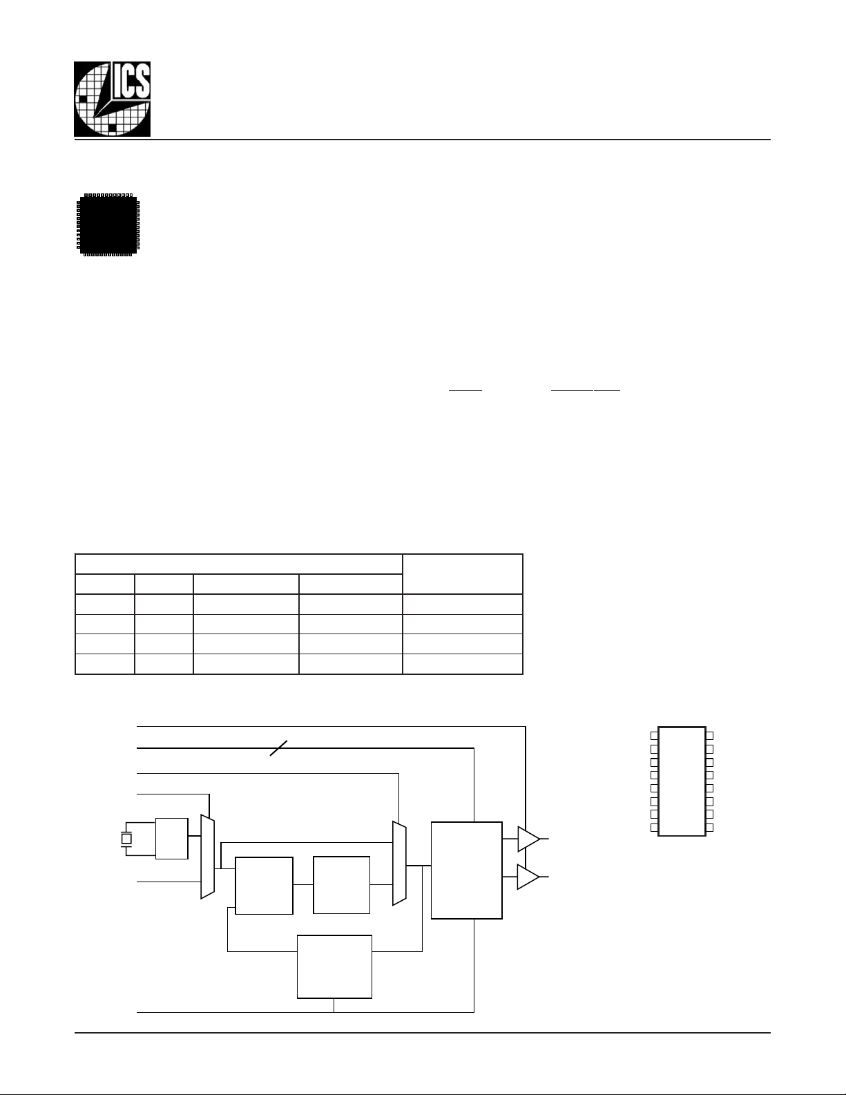
GENERAL DESCRIPTION
ICS
HiPerClockS™
parallel resonant crystal, the following frequencies can be
generated based on the 2 frequency select pins (F_SEL1:0):
156.25MHz, 125MHz, and 62.5MHz. The ICS840002-01 uses
ICS’ 3
achieve 1ps or lower typical random rms phase jitter, easily
meeting Ethernet jitter requirements. The ICS840002-01 is
packaged in a small 16-pin TSSOP package.
FREQUENCY SELECT FUNCTION TABLE
00 524 52.651
01 525 521
10 52015.26
11 525 521
The ICS840002-01 is a 2 output LVCMOS/LVTTL
Synthesizer optimized to generate Ethernet
reference clock frequencies and is a member of
TM
the HiPerClocks
family of high performance
clock solutions from ICS. Using a 25MHz 18pF
rd
generation low phase noise VCO technology and can
stupnI
1LES_F0LES_FeulaVrediviDMeulaVrediviDN
FEATURES
• Two LVCMOS/LVTTL outputs @ 3.3V,
17Ω typical output impedance
• Selectable crystal oscillator interface
or LVCMOS/LVTTL single-ended input
• Output frequency range: 56MHz - 175MHz
• VCO range: 560MHz - 700MHz
• Output skew: 12ps (maximum)
• RMS phase jitter at 156.25MHZ (1.875MHz - 20MHz):
0.47ps (typical)
Phase noise:
Offset Noise Power
100Hz ............... -97.4 dBc/Hz
1kHz .............. -120.2 dBc/Hz
10kHz .............. -127.6 dBc/Hz
100kHz ..............-126.1 dBc/Hz
• Full 3.3V or 3.3V core/2.5V output supply mode
• -30°C to 85°C ambient operating temperature
• Available in both standard and lead-free RoHS compliant
packages
ycneuqerFtuptuO
).feRzHM52(
BLOCK DIAGRAM PIN ASSIGNMENT
Pullup
OE
Phase
2
M = ÷25 (fixed)
VCO
1
F_SEL1:0
N
0 0 ÷4
0 1 ÷5
1 0 ÷10
1 1 ÷5
1
0
Q0
Q1
F_SEL1:0
nPLL_SEL
nXTAL_SEL
XTAL_IN
XTAL_OUT
TEST_CLK
840002AG-01 www.icst.com/products/hiperclocks.html REV. B JANUARY 13, 2006
Pullup:Pullup
Pulldown
Pulldown
Pulldown
Pulldown
MR
25MHz
OSC
0
1
Detector
F_SEL0
nXTAL_SEL
TEST_CLK
nPLL_SEL
4.4mm x 5.0mm x 0.92mm
1
16
15
14
13
12
11
10
9
F_SEL1
GND
GND
Q0
Q1
V
XTAL_IN
XTAL_OUT
V
OE
MR
DDA
VDD
2
3
4
5
6
7
8
ICS840002-01
16-Lead TSSOP
package body
G Package
Top View
DDO
Page 2
Integrated
Circuit
FEMTOCLOCKS™ C RYSTAL-TO-
Systems, Inc.
LVCMOS/LVTTL FREQUENCY SYNTHESIZER
TABLE 1. PIN DESCRIPTIONS
rebmuNemaNepyTnoitpircseD
10LES_FtupnIpulluP.slevelecafretniLTTVL/SOMCVL.niptcelesycneuqerF
2LES_LATXntupnInwodll
3KLC_TSETtupnInwodlluP.tupnikcolcLTTVL/SOMCVLdedne-elgniS
4EOtup
5RMtupnInwodlluP
6LES_LLPntupnInwodlluP
7V
8V
,9
01
11V
31,210Q,1QtuptuO .slevelecafretniLTTVL/SOMCVL.stuptuokcolcdedne-elgniS
51,41DNGrewoP.dnu
611LES_FtupnIpulluP.slevelecafretniLTTVL/SOMCVL.niptcelesycneuqerF
:ETON pulluP dna nwodlluP .se
ADD
DD
NI_LATX
ODD
nIpulluP
,TUO_LATX
uP
rewoP.nipylppusgolanA
rewoP.nipylppuseroC
tupnI
rewoP.nipylppustuptuO
.slevelecafretniLTTVL/SOMCVL.stupni
depmihgihanierastuptuo
sredivid
dessapybsiLLPeht,HGIHnehW
.slevelecafretniLTTVL/SOMCVL
NI_LATX
.tupniehtsi
orgylppusrewoP
ICS840002-01
ecnereferLLPehtsastupniKLC_TSETrolatsyrcehtneewtebstceleS
LATXstceles,WOLnehW.KLC_TSETstceles,HGIHnehW.ecruos
eht,WOLnehW.evitcaerastuptuoeht,HGIHnehW.nipelbanetuptuO
erasredividlanretnieht,HGIHcigolnehW.teseRretsaMHGIHevitcA
eht,WOLcigolnehW.wologotstuptuoevitcagnisuacteser
.redividtuptuoN/ycneuqerfkcolcecnerefer
.tuptuoehtsiTUO_LATX.ecafretnirotallicsolatsyrC
ulavlacipytrof,scitsiretcarahCniP,2elbaTeeS.srotsisertupnilanretniotrefer
lanretni
.slevelecafretniLTTVL/SOMCVL.delbaneerastuptuoehtdna
.tuptuoOCVehtmorfnevirdsituptuoeht,WOLnehW.ssapyBLLP
=ycneuqerftuptuoehtdna
.slevelecafretniLTTVL/SOMCVL.etatsecna
TABLE 2. PIN CHARACTERISTICS
lobmySretemaraPsnoitidnoCtseTmuminiMlacipyTmumixaMstinU
C
NI
C
DP
R
PULLUP
R
R
840002AG-01 www.icst.com/products/hiperclocks.html REV. B JANUARY 13, 2006
NWODLLUP
TUO
ecnaticapaCtupnI 4Fp
ecnaticapaCnoitapissiDrewoP 8Fp
rotsiseRpulluPtupnI 15kΩ
rotsiseRnwodlluPtupnI 15kΩ
ecnadepmItuptuO
%5±V3.3417112
%5±V5.2611252
2
Ω
Ω
Page 3
Integrated
Circuit
Systems, Inc.
ABSOLUTE MAXIMUM RATINGS
ICS840002-01
FEMTOCLOCKS™ C RYSTAL-TO-
LVCMOS/LVTTL FREQUENCY SYNTHESIZER
Supply Voltage, V
Inputs, V
Outputs, V
I
O
DD
4.6V
-0.5V to V
-0.5V to V
+ 0.5 V
DD
DDO
+ 0.5V
Package Thermal Impedance, θJA 89°C/W (0 lfpm)
Storage Temperature, T
STG
TABLE 3A. POWER SUPPLY DC CHARACTERISTICS, V
-65°C to 150°C
DD
lobmySretemaraPsnoitidnoCtseTmuminiMlacipyTmumixaMstinU
V
DD
V
ADD
V
ODD
I
DD
I
ADD
I
ODD
egatloVylppuSeroC 531.33.3564.3V
egatloVylppuSgolanA 531.33.3564.3V
egatloVylppuStuptuO
tnerruCylppuSrewoP 001Am
tnerruCylppuSgolanA 21Am
tnerruCylppuStuptuO 5Am
TABLE 3B. LVCMOS/LVTTL DC CHARACTERISTICS, V
lobmySretemaraPsnoitidnoCtseTmuminiMlacipyTmumixaMstinU
V
HI
V
LI
I
HI
I
LI
V
HO
V
LO
tupnI
tupnI
egatloVhgiHtupnI 2V
egatloVwoLtupnI 3.0-8.0V
1LES_F,0LES_F,EO
tnerruChgiH
,RM,LES_LLPn
KLC_TSET,LES_LATXn
1LES_F,0LES_F,EO
tnerruCwoL
,RM,LES_LLPn
KLC_TSET,LES_LATXn
1ETON;egatloVhgiHtuptuO
1ETON;egatloVwoLtuptuOV
05htiwdetanimretstuptuO:1ETON Ω Vot
ODD
= V
DD
V
V
DDA
= V
V
V
DD
DD
V
ODD
NOTE: Stresses beyond those listed under Absolute
Maximum Ratings may cause permanent damage to the
device. These ratings are stress specifications only. Functional
operation of product at these conditions or any conditions be-
yond those listed in the DC Characteristics or AC Character-
istics is not implied. Exposure to absolute maximum rating
conditions for extended periods may affect product reliability.
= 3.3V±5%, V
= 3.3V±5% OR 2.5V±5%, TA = 0°C TO 70°C
DDO
531.33.3564.3V
573.25.2526.2V
= 3.3V±5%, V
DDA
V=
DD
NI
= 3.3V±5% OR 2.5V±5%, TA = -30°C TO 85°C
DDO
DD
V564.3=
V526.2ro
V=
DD
NI
V564.3=
V526.2ro
,V526.2roV564.3=
V
V0=
NI
,V526.2roV564.3=
V
V0=
NI
ODD
V
ODD
%5±V564.3=6.2V
%5±V5.2=8.1V
051-Aµ
5-Aµ
%5±V5.2roV3.3=5.0V
3.0+V
5Aµ
051Aµ
.stiucriCtseTdaoLtuptuO,noitamrofnItnemerusaeMretemaraPeeS.2/
840002AG-01 www.icst.com/products/hiperclocks.html REV. B JANUARY 13, 2006
3
Page 4
Integrated
Circuit
Systems, Inc.
TABLE 4. CRYSTAL CHARACTERISTICS
retemaraPsnoitidnoCtseTmuminiMlacipyTmumixaMstinU
noitallicsOfoedoM latnemadnuF
ycneuqerF 52zHM
eireStnelaviuqE 05
ecnaticapaCtnuhS 7Fp
leveLevirD 1Wm
ICS840002-01
FEMTOCLOCKS™ C RYSTAL-TO-
LVCMOS/LVTTL FREQUENCY SYNTHESIZER
)RSE(ecnatsiseRs
.latsyrctnanoserlellarapFp81nagnisudeziretcarahC:ETON
Ω
TABLE 5A. AC CHARACTERISTICS, V
DD
= V
DDA
= V
= 3.3V±5%, TA = -30°C TO 85°C
DDO
lobmySretemaraPsnoitidnoCtseTmuminiMlacipyTmumixaMstinU
00=]0:1[LES_F041571zHM
f
TUO
ycneuqerFtuptuO
10=]0:1[LES_F211041zHM
11ro01=]0:1[LES_F6507zHM
t )o(ks3,1ETON;wekStuptuO 21sp
)zHM02-zHM578.1(zHM52.65174.0sp
t
t
Rt/F
)Ø(tij
2ETON
emiTllaF/esiRtuptuO%08ot%02002007sp
;)modnaR(rettiJesahPSMR
8.1(zHM5.2615.0sp
)zHM02-zHM578.1(zHM52175.0sp
)zHM02-zHM57
cdoelcyCytuDtuptuO 6445%
stuptuoneewtebwekssadenifeD:1ETON
.2/
VtaderusaeM
ODD
.tolPesioNesahPehtotreferesaelP:2ETON
.snoitidnocdaollauqehtiwdnasegatlovylppusemasehtta
.56dradnatSCEDEJhtiwecnadroccanidenifedsiretemarapsihT:3ETON
TABLE 5B. AC CHARACTERISTICS, V
DD
= V
DDA
= 3.3V±5%, V
= 2.5V±5%, TA = -30°C TO 85°C
DDO
lobmySretemaraPsnoitidnoCtseTmuminiMlacipyTmumixaMstinU
00=]0:1[LES_F041571zHM
f
TUO
ycneuqerFtuptuO
10=]0:1[LES_F211041zHM
11ro01=]0:1[LES_F6586zHM
t )o(ks3,1ETON;wekStuptuO 21sp
)zHM02-zHM578.1(zHM52.65174.0sp
t
t
Rt/F
)Ø(tij
2ETON
emiTllaF/esiRtuptuO%08ot%02002007sp
;)modnaR(rettiJesahPSMR
8.1(zHM5.2694.0sp
)zHM02-zHM578.1(zHM52155.0sp
)zHM02-zHM57
cdoelcyCytuDtuptuO 6445%
stuptuoneewtebwekssadenifeD:1ETON
.2/
VtaderusaeM
ODD
.tolPesioNesahPehtotreferesaelP:2ETON
.snoitidnocdaollauqehtiwdnasegatlovylppusemasehtta
.56dradnatSCEDEJhtiwecnadroccanidenifedsiretemarapsihT:3ETON
840002AG-01 www.icst.com/products/hiperclocks.html REV. B JANUARY 13, 2006
4
Page 5

Integrated
Circuit
Systems, Inc.
Hz
dBc
NOISE POWER
ICS840002-01
FEMTOCLOCKS™ C RYSTAL-TO-
LVCMOS/LVTTL FREQUENCY SYNTHESIZER
TYPICAL PHASE NOISE AT 62.5MHZ @3.3V
0
-10
-20
-30
-40
-50
-60
-70
-80
-90
-100
-110
-120
-130
-140
-150
-160
-170
-180
-190
100 1k 10k 100k 1M 10M 100M
Raw Phase Noise Data
➤
1.875MHz to 20MHz = 0.51ps (typical)
➤
Phase Noise Result by adding
1Gb Ethernet Filter to raw data
OFFSET FREQUENCY (HZ)
➤
1Gb Ethernet Filter
62.5MHz
RMS Phase Jitter (Random)
TYPICAL PHASE NOISE AT 156.25MHZ @3.3V
0
-10
-20
-30
-40
-50
1.875MHz to 20MHz = 0.47ps (typical)
➤
Phase Noise Result by adding
10Gb Ethernet Filter to raw data
dBc
NOISE POWER
Hz
-60
-70
-80
-90
-100
-110
-120
-130
-140
-150
-160
-170
-180
-190
100 1k 10k 100k 1M 10M 100M
Raw Phase Noise Data
➤
OFFSET FREQUENCY (HZ)
840002AG-01 www.icst.com/products/hiperclocks.html REV. B JANUARY 13, 2006
5
➤
10Gb Ethernet Filter
156.25MHz
RMS Phase Jitter (Random)
Page 6

Integrated
k
Circuit
Systems, Inc.
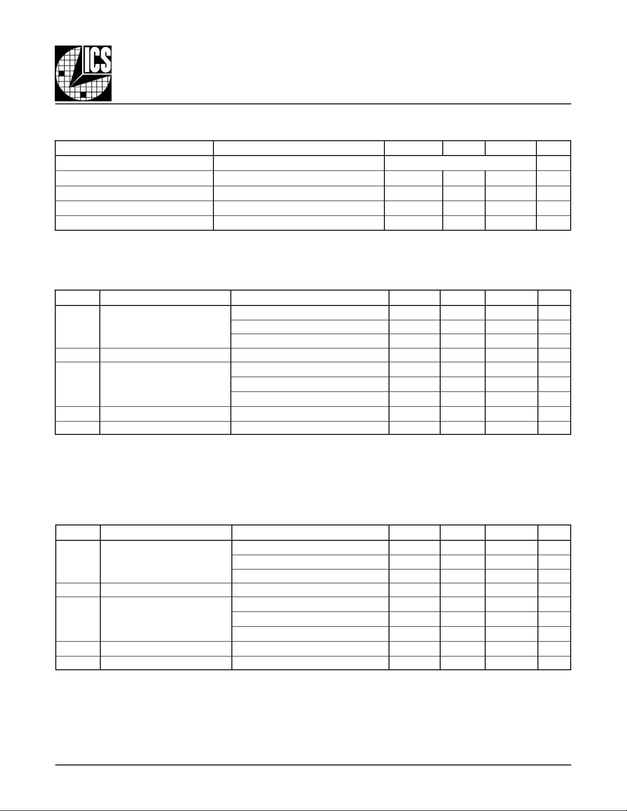
PARAMETER MEASUREMENT INFORMATION
ICS840002-01
FEMTOCLOCKS™ C RYSTAL-TO-
LVCMOS/LVTTL FREQUENCY SYNTHESIZER
1.65V±5%
VDD,
V
, V
DDA
DDO
LVCMOS
GND
-1.65V±5%
Phase Noise Plot
Noise Power
Offset Frequency
f
1
Qx
Phase Noise Mas
f
2
SCOPE
2.05V±5%
,
V
DD
V
DDA
LVCMOS
3.3V CORE/2.5V OUTPUT LOAD AC TEST CIRCUIT3.3V CORE/3.3V OUTPUT LOAD AC TEST CIRCUIT
Qx
Qy
1.25V±5%
V
DDO
GND
-1.25V±5%
V
DDO
2
V
SCOPE
Qx
DDO
2
tsk(o)
RMS Jitter = Area Under the Masked Phase Noise Plot
RMS PHASE JITTER
80%
t
F
20%
Clock
Outputs
20%
80%
t
R
OUTPUT RISE/FALL TIME
840002AG-01 www.icst.com/products/hiperclocks.html REV. B JANUARY 13, 2006
OUTPUT SKEW
V
DDO
t
PERIOD
t
PW
t
PERIOD
2
Q0, Q1
t
PW
odc =
OUTPUT DUTY CYCLE/PULSE WIDTH/PERIOD
6
x 100%
Page 7
Integrated
Circuit
Systems, Inc.
APPLICATION INFORMATION
POWER SUPPLY FILTERING TECHNIQUES
As in any high speed analog circuitry, the power supply pins
are vulnerable to random noise. The ICS840002-01 provides
separate power supplies to isolate any high switching
, V
noise from the outputs to the internal PLL. V
should be individually connected to the power supply
plane through vias, and bypass capacitors should be
used for each pin. To achieve optimum jitter performance,
power supply isolation is required. Figure 1 illustrates how
a 10Ω resistor along with a 10µF and a .01μF bypass
capacitor should be connected to each V
sistor can also be replaced by a ferrite bead.
, and V
DD
DDA
. The 10Ω re-
DDA
DDO
ICS840002-01
FEMTOCLOCKS™ C RYSTAL-TO-
LVCMOS/LVTTL FREQUENCY SYNTHESIZER
3.3V
V
DD
.01μF
V
DDA
.01μF
FIGURE 1. POWER SUPPLY FILTERING
10Ω
10μF
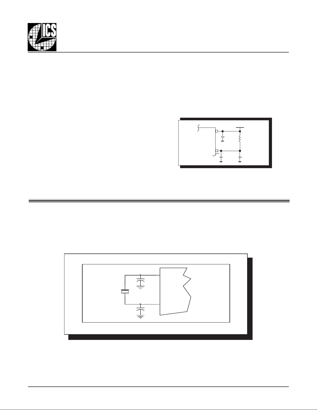
CRYSTAL INPUT INTERFACE
The ICS840002-01 has been characterized with 18pF paral-
lel resonant crystals. The capacitor values shown in Figure 2
C1
22p
18pF Parallel Cry stal
X1
C2
22p
Figure 2. CRYSTAL INPUt INTERFACE
below were determined using a 25MHz 18pF parallel resonant crystal and were chosen to minimize the ppm error.
XTA L_ I N
XTA L_ OU T
ICS84332
ICS840002-01
840002AG-01 www.icst.com/products/hiperclocks.html REV. B JANUARY 13, 2006
7
Page 8

Integrated
Circuit
Systems, Inc.
LVCMOS/LVTTL FREQUENCY SYNTHESIZER
RECOMMENDATIONS FOR UNUSED INPUT AND OUTPUT PINS
ICS840002-01
FEMTOCLOCKS™ C RYSTAL-TO-
INPUTS:
CRYSTAL INPUT:
For applications not requiring the use of the crystal oscillator
input, both XTAL_IN and XTAL_OUT can be left floating.
Though not required, but for additional protection, a 1kΩ
resistor can be tied from XTAL_IN to ground.
TEST_CLK I
NPUT:
For applications not requiring the use of the test clock, it can
be left floating. Though not required, but for additional
protection, a 1kΩ resistor can be tied from the TEST_CLK to
ground.
LVCMOS C
ONTROL PINS:
All control pins have internal pull-ups or pull-downs; additional
resistance is not required but can be added for additional
protection. A 1kΩ resistor can be used.
LAYOUT GUIDELINE
Figure 3 shows a schematic example of the ICS840002-01. An
example of LVCMOS termination is shown in this schematic.
Additional LVCMOS termination approaches are shown in the
LVCMOS Termination Application Note. In this example, an 18
pF parallel resonant 25MHz crystal is used. The C1=22pF and
OUTPUTS:
LVCMOS OUTPUT:
All unused LVCMOS output can be left floating. We
recommend that there is no trace attached.
C2=22pF are recommended for frequency accuracy. For different board layout, the C1 and C2 may be slightly adjusted for
optimizing frequency accuracy. 1KΩ pullup or pulldown resistors can be used for the logic control input pins.
Logic Control Input Examples
Set Logi c
VDD
Input to
'1'
RU1
1K
To Logic
Input
pins
RD1
Not Install
VDD
R1
10
If not using the cry st al i nput, it can be left floating.
For addit ional protec tion the XTAL_IN pin can be
tied to ground.
VDD
10uF
RU2
Not Install
RD2
1K
VDDA
C3
Set Logic
Input to
'0'
To Logic
Input
pins
C4
0.01u
U1
1
FSEL0
2
XTAL_SEL
3
TEST_CLK
4
OE
5
MR
6
nPLL_SEL
7
VDDA
8 9
VDD XTAL_OUT
C6
0.1u
ICS 840002-01
C2
22pF
FSEL1
GND
GND
VDDO
XTAL _ IN
XTA L 2
XTA L 1
C1
22pF
R2
33
Zo = 50 Ohm
VDD
LVCMOS
16
15
14
13
Q0
12
Q1
11
10
Zo = 50 Ohm
C5
0.1u
X1
VDD
R3
100
R4
100
LVCMOS
Optional Termination
Unused out put can be left float ing. There shoul d
no trac e att ached to unused out put. Device
charac teri zed with al l out puts terminat ed.
FIGURE 3. ICS840002-01 SCHEMATIC EXAMPLE
840002AG-01 www.icst.com/products/hiperclocks.html REV. B JANUARY 13, 2006
8
Page 9

Integrated
Circuit
Systems, Inc.
ICS840002-01
FEMTOCLOCKS™ C RYSTAL-TO-
LVCMOS/LVTTL FREQUENCY SYNTHESIZER
RELIABILITY INFORMATION
TABLE 6. θ
TRANSISTOR COUNT
The transistor count for ICS840002-01 is: 3085
VS
. AIR FLOW TABLE FOR 16 LEAD TSSOP
JA
θθ
θ
by Velocity (Linear Feet per Minute)
θθ
JA
Single-Layer PCB, JEDEC Standard Test Boards 137.1°C/W 118.2°C/W 106.8°C/W
Multi-Layer PCB, JEDEC Standard Test Boards 89.0°C/W 81.8°C/W 78.1°C/W
NOTE: Most modern PCB designs use multi-layered boards. The data in the second row pertains to most designs.
0 200 500
840002AG-01 www.icst.com/products/hiperclocks.html REV. B JANUARY 13, 2006
9
Page 10

Integrated
Circuit
Systems, Inc.
PACKAGE OUTLINE - G SUFFIX FOR 16 LEAD TSSOP
ICS840002-01
FEMTOCLOCKS™ C RYSTAL-TO-
LVCMOS/LVTTL FREQUENCY SYNTHESIZER
TABLE 7. PACKAGE DIMENSIONS
LOBMYS
N61
A--02.1
1A50.051.0
2A08.050.1
b91.003.0
c90.002.0
D09.401.5
ECISAB04.6
1E03.405.4
eCISAB56.0
L5
α
aaa--01.0
Reference Document: JEDEC Publication 95, MO-153
840002AG-01 www.icst.com/products/hiperclocks.html REV. B JANUARY 13, 2006
muminiMmumixaM
4.057.0
°0°8
10
sretemilliM
Page 11

Integrated
Circuit
Systems, Inc.
TABLE 8. ORDERING INFORMATION
rebmuNredrO/traPgnikraMegakcaPgnigakcaPgnippihSerutarepmeT
10-GA200048SCI10A20004POSSTdaeL61ebutC°58otC°03-
-GA200048SCI10A20004POSSTdaeL61leer&epat0052C°58otC°03-
T10
FL10-GA200048SCIL10A2000POSST"eerF-daeL"daeL61ebutC°58
TFL10-GA200048SCIL10A2000POSST"eerF-daeL"daeL61leer&epat0052C°58otC°03-
ICS840002-01
FEMTOCLOCKS™ C RYSTAL-TO-
LVCMOS/LVTTL FREQUENCY SYNTHESIZER
otC°03-
gifnoceerF-bPehterarebmuntrapehtotxiffus"FL"nahtiwderedroeratahtstraP:ETON
.tnailpmocSHoReradnanoitaru
The aforementioned trademarks, HiPerClockS and FEMTOCLOCKS are trademarks of Integrated Circuit Systems, Inc. or its subsidiaries in the United States and/or other countries.
While the information presented herein has been checked for both accuracy and reliability, Integrated Circuit Systems, Incorporated (ICS) assumes no responsibility for either its use
or for infringement of any patents or other rights of third parties, which would result from its use. No other circuits, patents, or licenses are implied. This product is intended for use
in normal commercial applications. Any other applications such as those requiring extended temperature range, high reliability, or other extraordinary environmental requirements are
not recommended without additional processing by ICS. ICS reserves the right to change any circuitry or specifications without notice. ICS does not authorize or warrant any ICS
product for use in life support devices or critical medical instruments.
840002AG-01 www.icst.com/products/hiperclocks.html REV. B JANUARY 13, 2006
11
Page 12

Integrated
Circuit
FEMTOCLOCKS™ C RYSTAL-TO-
ICS840002-01
Systems, Inc.
LVCMOS/LVTTL FREQUENCY SYNTHESIZER
TEEHSYROTSIHNOISIVER
veRelbaTegaPegnahCfonoitpircseDetaD
1
B
4T
8T
4
8
11
ClatsyrC
deddA .sniPtuptuOdnatupnIdesunUrofsnoitadnemmoceR
niredrO
tcerroc-noitceSserutaeF
.tellubrettijesahpSMRehtnizHM02-zHM578.1ot
.leveLevirDdedda-elbaTscitsiretcarah
dnagnikramdradnatsdetcerroc-elbaTnoitamrofnIg
.etondnagnikram,rebmuntrapeerF-daeLdedda
zHM571-zHM578.1morfegnarnoitargetniehtde
60/31/1
840002AG-01 www.icst.com/products/hiperclocks.html REV. B JANUARY 13, 2006
12
 Loading...