

Page 1
Integrated
Circuit
Systems, Inc.
ICS83058I
8:1, SINGLE-ENDED MULTIPLEXER
GENERAL DESCRIPTION
ICS
HiPerClockS™
output. The output has a V
2.5V, or 1.8V, making the device ideal for use in voltage translation applications. An output enable pin places the output in
a high impedance state which may be useful for testing or
debug. The device operates up to 250MHz and is packaged
in a 16 TSSOP.
The ICS83058I is a low skew, 8:1, Single-ended
Multiplexer and a member of the HiPerClockS™
family of High Performance Clock Solutions from
ICS. The ICS83058I has eight selectable singleended clock inputs and one single-ended clock
pin which may be set at 3.3V,
DDO
FEATURES
• 8:1 single-ended multiplexer
DD
DDO
= V
=3 .3V)
DDO
= 3.3V
DDO
= V
DD
= 3.3V
= 3.3V
DDO
• Q nominal output impedance: 7Ω (V
• Maximum output frequency: 250MHz
• Propagation delay: 3ns (maximum), VDD = V
• Input skew: 225ps (maximum), V
• Part-to-part skew: 475ps (maximum), V
• Operating supply modes:
VDD/V
DDO
3.3V/3.3V
3.3V/2.5V
3.3V/1.8V
2.5V/2.5V
2.5V/1.8V
• -40°C to 85°C ambient operating temperature
• Available in both standard and lead-free RoHS-compliant
packages
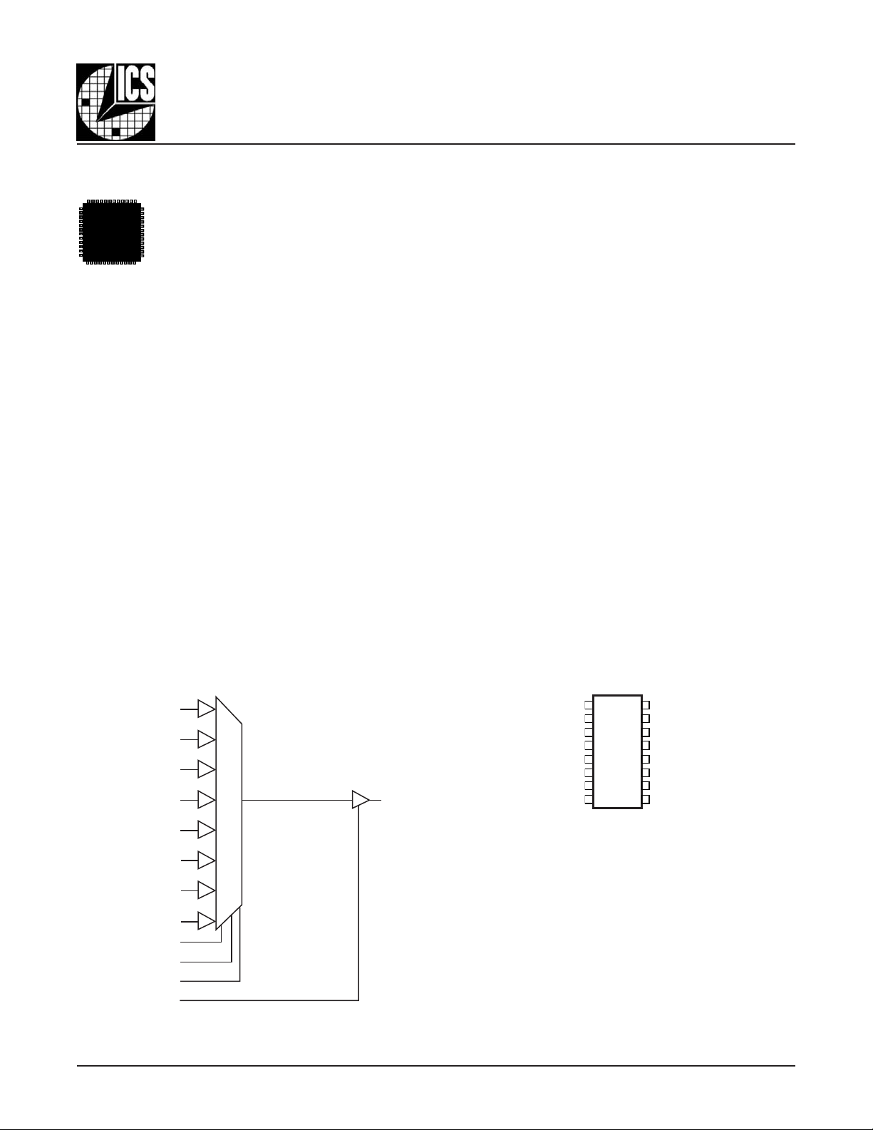
BLOCK DIAGRAM PIN ASSIGNMENT
1
CLK0
CLK1
CLK2
CLK3
CLK4
CLK5
CLK6
CLK7
SEL2
SEL1
SEL0
OE
83058AGI www.icst.com/products/hiperclocks.html REV. A SEPTEMBER 27, 2005
Q
4.4mm x 5.0mm x 0.92mm package body
1
Q
CLK7
OE
CLK6
GND
CLK5
SEL2
CLK4
ICS83058I
16-Lead TSSOP
16
2
15
3
14
4
13
5
12
6
11
7
10
8
9
G Package
Top View
V
DDO
CLK0
SEL0
CLK1
V
DD
CLK2
SEL1
CLK3
Page 2

Integrated
Circuit
Systems, Inc.
TABLE 1. PIN DESCRIPTIONS
rebmuNemaNepyTnoitpircseD
1QtuptuO .slevelecafretniLTTVL/SOMCVL.tuptuokcolcdedne-elgniS
,4,2
,8,6
,11,9
51,31
3EOt
5DNGrewoP.dnuorgylppusrewoP
,01,7
41
21V
61V
:ETON pulluP dna nwodlluP .seulavlacipytrof,scitsiretcarahCniP,2elbaTeeS.srotsisertup
TABLE 2. PIN CHARACTERISTICS
LC,7KLC
0KLC,1KLC
0LES
DD
ODD
ICS83058I
8:1, SINGLE-ENDED MULTIPLEXER
,6K
,4KLC,5KLC
,2KLC,3KLC
,1LES,2LES
tupnInwodlluP.slevelecafretniLTTVL/SOMCVL.stupnikcolcdedne-elgniS
upnIpulluP
tupnInwodlluP
rewoP.nipylppustupnidnaeroC
rewoP.nipylppustuptuO
nilanretniotrefer
.etatsecnadepmiHGIHnierastuptuo,WOLnehW.elbanetuptuO
uptuo,HGIHnehW
tupnitceleskcolC
.elbaTnoitcnuFtupnIlortnoCeeS.
.slevelecafretniLTTVL/SOMCVL.evitcaerast
.slevelecafretniLTTVL/SOMCVL
lobmySretemaraPsnoitidnoCtseTmuminiMlacipyTmumixaM
C
NI
R
PULLUP
R
C
R
NWODLLUP
DP
TUO
ecnaticapaCtupnI 4Fp
rotsiseRpulluPtupnI 15kΩ
rotsiseRnwodlluPtupnI 15kΩ
)tuptuorep(
ecnadepmItuptuO
TABLE 3. CONTROL INPUT FUNCTION TABLE
stupnIlortnoC
2LES1LES0LES
000 0KLC
00 1 1KLC
010 2KLC
011 3KLC
10 0 4KLC
10 1 5KLC
110 6KLC
111 7KLC
stinU
V
ecnaticapaCnoitapissiDrewoP
ODD
V
ODD
V
ODD
V
ODD
V
ODD
V
ODD
V564.3=81Fp
V526.2=02Fp
V98.1=03Fp
V564.3=7
V526.2=7
V98.1=01
Ω
Ω
Ω
QotdetceleStupnI
83058AGI www.icst.com/products/hiperclocks.html REV. A SEPTEMBER 27, 2005
2
Page 3
Integrated
Circuit
Systems, Inc.
ABSOLUTE MAXIMUM RATINGS
ICS83058I
8:1, SINGLE-ENDED MULTIPLEXER
Supply Voltage, V
Inputs, V
I
Outputs, V
DD
O
Package Thermal Impedance, θ
Storage Temperature, T
STG
4.6V
-0.5V to V
-0.5V to V
89°C/W (0 lfpm)
JA
-65°C to 150°C
DD
DDO
TABLE 4A. POWER SUPPLY DC CHARACTERISTICS, V
lobmySretemaraPsnoitidnoCtseTmuminiMlacipyTmumixaMstinU
V
DD
V
ODD
I
DD
I
ODD
egatloVylppuSeroC 531.33.3564.3V
egatloVylppuStuptuO 531.33.3564.3V
tnerruCylppuSrewoP 04Am
tnerruCylppuStuptuO 5Am
TABLE 4B. POWER SUPPLY DC CHARACTERISTICS, V
lobmySretemaraPsnoitidnoCtseTmuminiMlacipyTmumixaMstinU
V
DD
V
ODD
I
DD
I
ODD
egatloVylppuSeroC 531.33.3564.3V
egatloVylppuStuptuO 573.25.2526.2V
tnerruCylppuSrewoP 04Am
tnerruCylppuStuptuO 5Am
+ 0.5 V
+ 0.5V
= V
DD
= 3.3V±5%, V
DD
NOTE: Stresses beyond those listed under Absolute
Maximum Ratings may cause permanent damage to the
device. These ratings are stress specifications only. Functional
operation of product at these conditions or any conditions be-
yond those listed in the DC Characteristics or AC Character-
istics is not implied. Exposure to absolute maximum rating
conditions for extended periods may affect product reliability.
= 3.3V±5%, TA = -40°C TO 85°C
DDO
= 2.5V±5%, TA = -40°C TO 85°C
DDO
TABLE 4C. POWER SUPPLY DC CHARACTERISTICS, V
= 3.3V±5%, V
DD
= 1.8V±5%, TA = -40°C TO 85°C
DDO
lobmySretemaraPsnoitidnoCtseTmuminiMlacipyTmumixaMstinU
V
DD
V
ODD
I
DD
I
ODD
TABLE 4D. POWER SUPPLY DC CHARACTERISTICS, V
egatloVylppuSeroC 531.33.3564.3V
egatloVylppuStuptuO 17.18.198.1V
tnerruCylppuSrewoP 04Am
tnerruCylppuStuptuO 5Am
= V
DD
= 2.5V±5%, TA = -40°C TO 85°C
DDO
lobmySretemaraPsnoitidnoCtseTmuminiMlacipyTmumixaMstinU
V
DD
V
ODD
I
DD
I
ODD
TABLE 4E. POWER SUPPLY DC CHARACTERISTICS, V
egatloVylppuSeroC 573.25.2526.2V
egatloVylppuStuptuO 573.25.2526.2V
tnerruCylppuSrewoP 53Am
tnerruCylppuStuptuO 5Am
= 2.5V±5%, V
DD
= 1.8V±5%, TA = -40°C TO 85°C
DDO
lobmySretemaraPsnoitidnoCtseTmuminiMlacipyTmumixaMstinU
V
DD
V
ODD
I
DD
I
ODD
83058AGI www.icst.com/products/hiperclocks.html REV. A SEPTEMBER 27, 2005
egatloVylppuSeroC 573.25.2526.2V
egatloVylppuStuptuO 17.18.198.1V
tnerruCylppuSrewoP 53Am
tnerruCylppuStuptuO 5Am
3
Page 4
Integrated
Circuit
Systems, Inc.
TABLE 4F. LVCMOS/LVTTL DC CHARACTERISTICS, TA = -40°C TO 85°C
lobmySretemaraPsnoitidnoCtseTmuminiMlacipyTmumixaMstinU
V
V
HI
V
LI
egatloVhgiHtupnI
egatloVwoLtupnI
,7KLC:0KLC
I
HI
tnerruChgiHtupnI
2LES:0LES
EOV
,7KLC:0KLC
I
LI
tnerruCwoLtupnI
2LES:0LES
EOV
V
V
HO
hgiHtuptuOegatloV
V
V
V
V
LO
egatloVwoLtuptuO
V
V
05htiwdetanimretstuptuO:1ETON Ω Vot
ODD
DD
V
DD
V
DD
V
DD
V
DD
DD
V
DD
DD
ODD
ODD
ODD
ODD
ODD
ODD
ICS83058I
8:1, SINGLE-ENDED MULTIPLEXER
%5±V3.3=2V
%5±V5.2=7.1V
%5±V3.3=3.0-8.0V
%5±V5.2=3.0-7.0V
%5±V5.2roV3.3=051Aµ
%5±V5.2roV3.3=5Aµ
%5±V5.2roV3.3=5-Aµ
%5±V5.2roV3.3=051-Aµ
1ETON;%5±V3.3=6.2V
1ETON;%5±V5.2=8.1V
1ETON;%5±V8.1=V
3.0-V
DD
1ETON;%5±V3.3=5.0V
1ETON;%5±V5.2=54.0V
1ETON;%5±V8.1=53.0V
3.0+V
DD
3.0+V
DD
.smargaid"tiucriCtseTdaoL",noitcestnemerusaeMretemaraPeeS.2/
TABLE 5A. AC CHARACTERISTICS, V
= V
DD
= 3.3V ± 5%, TA = -40°C TO 85°C
DDO
lobmySretemaraPsnoitidnoCtseTmuminiMlacipyTmumixaMstinU
f
XAM
pt
HL
pt
LH
ycneuqerFtuptuO 052zHM
1ETON;hgiHotwoL,yaleDnoitagaporP 4.27.20.3sn
1ETON;woLothgiH,yaleDnoitagaporP 5.27.29.2sn
t )i(ks2ETON;wekStupnI 55522sp
t )pp(ks3,2ETON;wekStraP-ot-traP 574sp
t
Rt/F
emiTllaF/esiRtuptuO%08ot%0205005sp
cdoelcyCytuDtuptuO 5455%
XUM
LOSI
noitalosIXUMzHM001@54Bd
VmorfderusaeM:1ETON
DD
Vottupniehtfo2/
ODD
pytemasehtgnisU.snoitidnocdaollauqehtiw
.tuptuoehtfo2/
.56dradnatSCEDEJhtiwecnadroccanidenifedsiretemarapsihT:2ETON
itareposecivedtnereffidnostuptuoneewtebwekssadenifeD:3ETON
dnasegatlovylppusemasehtagn
.2/
Vtaderusaemsituptuoeht,ecivedhcaenotupnifoe
83058AGI www.icst.com/products/hiperclocks.html REV. A SEPTEMBER 27, 2005
4
Page 5

Integrated
Circuit
Systems, Inc.
ICS83058I
8:1, SINGLE-ENDED MULTIPLEXER
TABLE 5B. AC CHARACTERISTICS, V
= 3.3V ± 5%, V
DD
= 2.5V ± 5%, TA = -40°C TO 85°C
DDO
lobmySretemaraPsnoitidnoCtseTmuminiMlacipyTmumixaMstinU
f
XAM
pt
HL
pt
LH
ycneuqerFtuptuO 052zHM
1ETON;hgiHotwoL,yaleDnoitagaporP 5.28.21.3sn
1ETON;woLothgiH,yaleDnoitagaporP 6.28.20.3sn
t )i(ks2ETON;wekStupnI 54051sp
t )pp(ks3,2ETON;wekStraP-ot-traP 004sp
t
Rt/F
emiTllaF/esiRtuptuO%08ot%0205005sp
cdoelcyCytuDtuptuO 5455%
XUM
LOSI
TABLE 5C. AC CHARACTERISTICS, V
noitalosIXUMzHM001@54Bd
VmorfderusaeM:1ETON
DD
Vottupniehtfo2/
ODD
pytemasehtgnisU.snoitidnocdaollauqehtiw
= 3.3V ± 5%, V
DD
= 1.8V ± 5%, TA = -40°C TO 85°C
DDO
.tuptuoehtfo2/
.56dradnatSCEDEJhtiwecnadroccanidenifedsiretemarapsihT:2ETON
itareposecivedtnereffidnostuptuoneewtebwekssadenifeD:3ETON
dnasegatlovylppusemasehtagn
.2/
Vtaderusaemsituptuoeht,ecivedhcaenotupnifoe
lobmySretemaraPsnoitidnoCtseTmuminiMlacipyTmumixaMstinU
f
XAM
pt
HL
pt
LH
ycneuqerFtuptuO 052zHM
1ETON;hgiHotwoL,yaleDnoitagaporP 7.22.38.3sn
1ETON;woLothgiH,yaleDnoitagaporP 8.23.38.3sn
t )i(ks2ETON;wekStupnI 05051sp
t )pp(ks3,2ETON;wekStraP-ot-traP 574sp
t
Rt/F
emiTllaF/esiRtuptuO%08ot%02001007sp
cdoelcyCytuDtuptuO 5455%
XUM
LOSI
noitalosIXUMzHM001@54Bd
VmorfderusaeM:1ETON
DD
Vottupniehtfo2/
ODD
pytemasehtgnisU.snoitidnocdaollauqehtiw
.tuptuoehtfo2/
.56dradnatSCEDEJhtiwecnadroccanidenifedsiretemarapsihT:2ETON
itareposecivedtnereffidnostuptuoneewtebwekssadenifeD:3ETON
dnasegatlovylppusemasehtagn
.2/
Vtaderusaemsituptuoeht,ecivedhcaenotupnifoe
83058AGI www.icst.com/products/hiperclocks.html REV. A SEPTEMBER 27, 2005
5
Page 6
Integrated
Circuit
Systems, Inc.
ICS83058I
8:1, SINGLE-ENDED MULTIPLEXER
TABLE 5D. AC CHARACTERISTICS, V
= V
DD
= 2.5V ± 5%, TA = -40°C TO 85°C
DDO
lobmySretemaraPsnoitidnoCtseTmuminiMlacipyTmumixaMstinU
f
XAM
pt
HL
pt
LH
ycneuqerFtuptuO 052zHM
1ETON;hgiHotwoL,yaleDnoitagaporP 5.20.35.3sn
1ETON;woLothgiH,yaleDnoitagaporP 5.29.24.3sn
t )i(ks2ETON;wekStupnI 06571sp
t )pp(ks3,2ETON;wekStraP-ot-traP 003sp
t
Rt/F
emiTllaF/esiRtuptuO%08ot%02001005sp
cdoelcyCytuDtuptuO 0406%
XUM
LOSI
TABLE 5E. AC CHARACTERISTICS, V
noitalosIXUMzHM001@54Bd
VmorfderusaeM:1ETON
DD
Vottupniehtfo2/
ODD
pytemasehtgnisU.snoitidnocdaollauqehtiw
= 2.5V ± 5%, V
DD
= 1.8V ± -5%, TA = -40°C TO 85°C
DDO
.tuptuoehtfo2/
.56dradnatSCEDEJhtiwecnadroccanidenifedsiretemarapsihT:2ETON
itareposecivedtnereffidnostuptuoneewtebwekssadenifeD:3ETON
dnasegatlovylppusemasehtagn
.2/
Vtaderusaemsituptuoeht,ecivedhcaenotupnifoe
lobmySretemaraPsnoitidnoCtseTmuminiMlacipyTmumixaMstinU
f
XAM
pt
HL
pt
LH
ycneuqerFtuptuO 052zHM
1ETON;hgiHotwoL,yaleDnoitagaporP 6.23.30.4sn
1ETON;woLothgiH,yaleDnoitagaporP 7.23.30.4sn
t )i(ks2ETON;wekStupnI 05051sp
t )pp(ks3,2ETON;wekStraP-ot-traP 523sp
t
Rt/F
emiTllaF/esiRtuptuO%08ot%02001007sp
cdoelcyCytuDtuptuO 0406%
XUM
LOSI
noitalosIXUMzHM001@54Bd
VmorfderusaeM:1ETON
DD
Vottupniehtfo2/
ODD
pytemasehtgnisU.snoitidnocdaollauqehtiw
.tuptuoehtfo2/
.56dradnatSCEDEJhtiwecnadroccanidenifedsiretemarapsihT:2ETON
itareposecivedtnereffidnostuptuoneewtebwekssadenifeD:3ETON
dnasegatlovylppusemasehtagn
.2/
Vtaderusaemsituptuoeht,ecivedhcaenotupnifoe
83058AGI www.icst.com/products/hiperclocks.html REV. A SEPTEMBER 27, 2005
6
Page 7

Integrated
Circuit
Systems, Inc.
PARAMETER MEASUREMENT INFORMATION
ICS83058I
8:1, SINGLE-ENDED MULTIPLEXER
1.65V±5%
VDD,
V
DDO
LVCMOS
GND
-1.65V±5%
SCOPE
Qx
3.3V CORE/3.3V OUTPUT LOAD AC TEST CIRCUIT
2.05V±5%
1.25V±5%
V
DD
V
LVCMOS
GND
DDO
Qx
SCOPE
1.25V±5%
VDD,
V
DDO
LVCMOS
GND
-1.25V±5%
SCOPE
Qx
2.5V CORE/2.5V OUTPUT LOAD AC TEST CIRCUIT
2.4±5%
V
0.9V±5%
DD
V
DDO
LVCMOS
GND
SCOPE
Qx
Part 1
Qx
Part 2
Qy
-0.9V±5%
V
DDO
2
V
DDO
2
tsk(pp)
-1.25V±5%
3.3V CORE/2.5V OUTPUT LOAD AC TEST CIRCUIT
1.6V±5%
0.9V±5%
V
DD
V
LVCMOS
GND
-0.9V±5%
DDO
Qx
3.3V CORE/1.8V OUTPUT LOAD AC TEST CIRCUIT
SCOPE
2.5 CORE/1.8V OUTPUT LOAD AC TEST CIRCUIT PART-TO-PART SKEW
83058AGI www.icst.com/products/hiperclocks.html REV. A SEPTEMBER 27, 2005
7
Page 8

CLK0:CLK7
Q
Integrated
Circuit
Systems, Inc.
V
DD
2
V
DDO
2
tp
LH
ICS83058I
8:1, SINGLE-ENDED MULTIPLEXER
V
DD
2
V
DDO
2
tp
HL
Clock
Outputs
20%
80%
t
R
80%
t
F
20%
CLKx
Q
CLKy
Q
INPUT SKEW
t
t
PD1
PD2
tsk(i) = ⏐t
PD2
– t
PD1
OUTPUT RISE/FALL TIMEPROPAGATION DELAY
V
DDO
t
PERIOD
t
PW
t
PERIOD
2
x 100%
Q
t
PW
odc =
⏐
OUTPUT DUTY CYCLE/PULSE WIDTH/PERIOD
83058AGI www.icst.com/products/hiperclocks.html REV. A SEPTEMBER 27, 2005
8
Page 9

Integrated
Circuit
Systems, Inc.
APPLICATION INFORMATION
RECOMMENDATIONS FOR UNUSED INPUT PINS
INPUTS:
ICS83058I
8:1, SINGLE-ENDED MULTIPLEXER
CLK INPUT:
For applications not requiring the use of a clock input, it can
be left floating. Though not required, but for additional
protection, a 1kW resistor can be tied from the CLK input to
ground.
LVCMOS CONTROL PINS:
All control pins have internal pull-ups or pull-downs;
additional resistance is not required but can be added for
additional protection. A 1kΩ resistor can be used.
83058AGI www.icst.com/products/hiperclocks.html REV. A SEPTEMBER 27, 2005
9
Page 10

Integrated
Circuit
Systems, Inc.
ICS83058I
8:1, SINGLE-ENDED MULTIPLEXER
RELIABILITY INFORMATION
TABLE 6. θ
TRANSISTOR COUNT
The transistor count for ICS83058I is: 874
VS
. AIR FLOW TABLE FOR 16 LEAD TSSOP
JA
θθ
θ
θθ
Single-Layer PCB, JEDEC Standard Test Boards 137.1°C/W 118.2°C/W 106.8°C/W
Multi-Layer PCB, JEDEC Standard Test Boards 89.0°C/W 81.8°C/W 78.1°C/W
NOTE: Most modern PCB designs use multi-layered boards. The data in the second row pertains to most designs.
by Velocity (Linear Feet per Minute)
JA
0 200 500
83058AGI www.icst.com/products/hiperclocks.html REV. A SEPTEMBER 27, 2005
10
Page 11

Integrated
Circuit
Systems, Inc.
PACKAGE OUTLINE - G SUFFIX FOR 16 LEAD TSSOP
ICS83058I
8:1, SINGLE-ENDED MULTIPLEXER
TABLE 7. PACKAGE DIMENSIONS
LOBMYS
N61
A--02.1
1A50.051.0
2A08.050.1
b91.003.0
c90.002.0
D09.401.5
ECISAB04.6
1E03.405.4
eCISAB56.0
L5
α
aaa--01.0
Reference Document: JEDEC Publication 95, MO-153
83058AGI www.icst.com/products/hiperclocks.html REV. A SEPTEMBER 27, 2005
muminiMmumixaM
4.057.0
°0°8
11
sretemilliM
Page 12
Integrated
Circuit
Systems, Inc.
TABLE 8. ORDERING INFORMATION
rebmuNredrO/traPgnikraMegakcaPgnigakcaPgnippihSerutarepmeT
IGA85038SCIIGA85038POSSTdaeL61ebutC°58otC°04-
038SCIIGA85038POSSTdaeL61leer&epat0052C°58otC°04-
5038SCIDBTPOSST"eerF-daeL"daeL61leer&epat0052C°58otC°04-
TIGA85
FLIGA85038SCIDBTPOSST"eerF-daeL"daeL61ebutC°58otC°04-
TFLIGA8
ICS83058I
8:1, SINGLE-ENDED MULTIPLEXER
muntrapehtotxiffus"FL"nahtiwderedroeratahtstraP:ETON
.tnailpmocSHoReradnanoitarugifnoceerF-bPehterareb
The aforementioned trademark, HiPerClockS™ is a trademark of Integrated Circuit Systems, Inc. or its subsidiaries in the United States and/or other countries.
While the information presented herein has been checked for both accuracy and reliability, Integrated Circuit Systems, Incorporated (ICS) assumes no responsibility for either its use
or for infringement of any patents or other rights of third parties, which would result from its use. No other circuits, patents, or licenses are implied. This product is intended for use
in normal commercial and industrial applications. Any other applications such as those requiring high reliability or other extraordinary environmental requirements are not
recommended without additional processing by ICS. ICS reserves the right to change any circuitry or specifications without notice. ICS does not authorize or warrant any ICS product
for use in life support devices or critical medical instruments.
83058AGI www.icst.com/products/hiperclocks.html REV. A SEPTEMBER 27, 2005
12
 Loading...