

Page 1
ICS7151
Spread Spectrum Clock Generator
Description
The ICS7151-10, -20, -40, and -50 are clock
generators for EMI (Electro Magnetic Interference)
reduction (see below for frequency ranges and
multiplier ratios). Spectral peaks can be attenuated by
slightly modulating the oscillation frequency. Both down
and center spread profiles are selectable. Down spread
maintains an average frequency less than an unspread
clock, and will not exceed the maximum frequency of
an unspread clock.
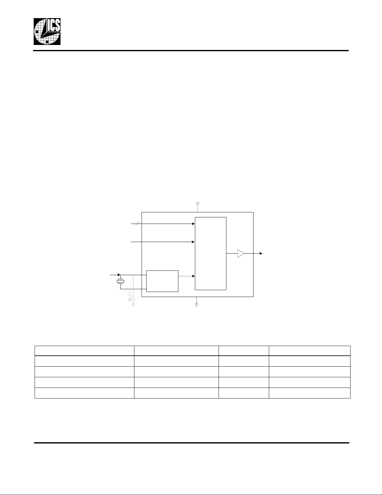
Block Diagram
2
S1:0
ENS
XIN
XOUT
Clock Buffer/
Crystal
Ocsillator
Features
• Operating voltage of 3.3 V ±0.3 V
• Packaged in 8-pin SOIC
• Available in Pb (lead) free package
• Input frequency range of 16.5 to 33.4 MHz
• Output frequency ranges of 8.3 to 16.7 MHz, 16.5 to
33.4 MHz, 33.3 to 66.7 MHz, 66.6 to 133.4 MHz
• Provides a spread spectrum clock output (±0.5%,
±1.5% center spread; -1.0%, -3.0% down spread)
• Multiplication rates of x1/2, x1, x2, and x4
• Advanced, low-power CMOS process
VDD
PLL Clock
Synthesis
and Spread
Spectrum
Circuitry
CKOUT
External caps required with crystal for
accurate tuning of the clock
GND
Product Lineup
Product Input Frequency Range Multiplier Ratio Output Frequency Range
ICS7151M-10, ICS7151MI-10 16.5 MHz to 33.4 MHz X1 16.5 MHz to 33.4 MHz
ICS7151M-20, ICS7151MI-20 16.5 MHz to 33.4 MHz X2 33.3 MHz to 66.7 MHz
ICS7151M-40, ICS7151MI-40 16.5 MHz to 33.4 MHz X4 66.6 MHz to 133.4 MHz
ICS7151M-50, ICS7151MI-50 16.5 MHz to 33.4 MHz X1/2 8.3 MHz to 16.7 MHz
MDS 7151 E 1 Revision 012306
Integrated Circuit Systems, Inc. ● 525 Race Street, San Jose, CA 95126 ● tel (408) 297-1201 ● www.icst.com
Page 2
ICS7151
Spread Spectrum Clock Generator
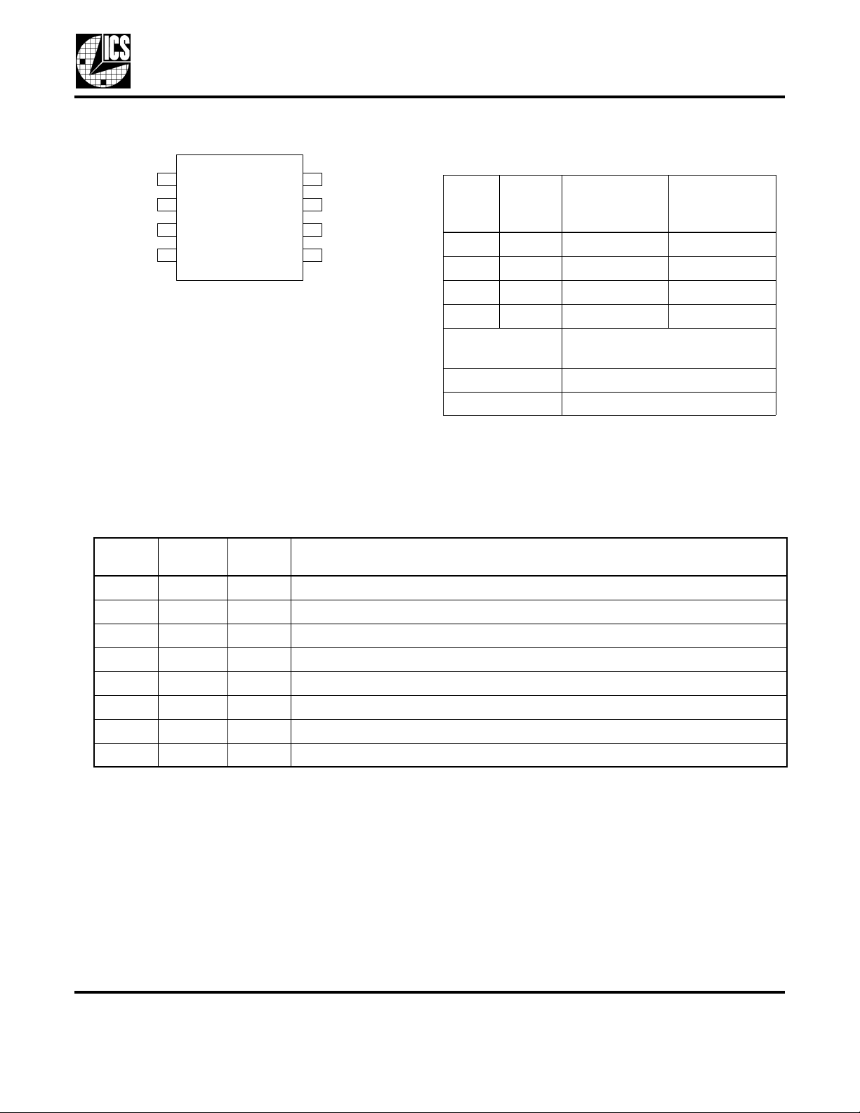
Pin Assignment Spread Direction and Percentage
Select Table
XOUT
XIN 1
GND
S0
S1
2
3
4
8
VDD
7
ENS
6
5
CKOUT
S1
Pin 4
(note1)
0 0 Center ±1.5
0 1 Center ±0.5
S0
Pin 3
(note1)
Spread
Direction
Percentage (%)
Spread
8 pin (150 mil) SOIC
Pin Descriptions
Pin
Number
1 XIN Input Resonator connection pin/clock input pin.
2 GND Power Connect to ground.
3 S0 Input Select pin 0. Modulation rate setting pin.
4 S1 Input Select pin 1. Modulation rate setting pin.
5 CKOUT Output Modulated clock output pin.
6 ENS Input Modulation enable setting pin. Internal pull-up resistor.
7 VDD Power Connect to +3.3 V.
Pin
Name
10 Down -1.0
1 1 Down -3.0
ENS
(note 2)
0
1
Notes:
1. The modulation rate varies with input frequency.
2. Spread will default to ON when ENS pin is left open.
Pin Type Pin Description
Spread Spectrum
OFF
ON
8 XOUT Output Resonator connection pin.
MDS 7151 E 2 Revision 012306
Integrated Circuit Systems, Inc. ● 525 Race Street, San Jose, CA 95126 ● tel (408) 297-1201 ● www.icst.com
Page 3

ICS7151
Spread Spectrum Clock Generator
External Components
The ICS7151 requires a minimum number of external
components for proper operation.
Decoupling Capacitor
A decoupling capacitor of 0.01µF must be connected
between GND and VDD on pin 7, as close to this pin as
possible. For optimum device performance, the
decoupling capacitor should be mounted on the
component side of the PCB. Avoid the use of vias in the
decoupling circuit.
Series Termination Resistor
Series termination should be used on the clock output.
To series terminate a 50Ω trace (a commonly used
trace impedance) place a 27Ω resistor in series with
the clock line, as close to the clock output pin as
possible. The nominal impedance of the clock output is
25Ω.
PCB Layout Recommendations
For optimum device performance and lowest output
phase noise, the following guidelines should be
observed.
underneath the device, or on layers adjacent to the
ground plane layer used by the device.
Crystal Information
The crystal used should be a fundamental mode (do
not use third overtone), parallel resonant. Crystal
capacitors should be connected from pins X1 to ground
and X2 to ground to optimize the initial accuracy. The
value of these capacitors is given by the following
equation:
Crystal caps (pF) = (C
In the equation, C
for a crystal with a 16 pF load capacitance, two 20 pF
[(16-6) x 2] capacitors should be used.
is the crystal load capacitance. So,
L
- 6) x 2
L
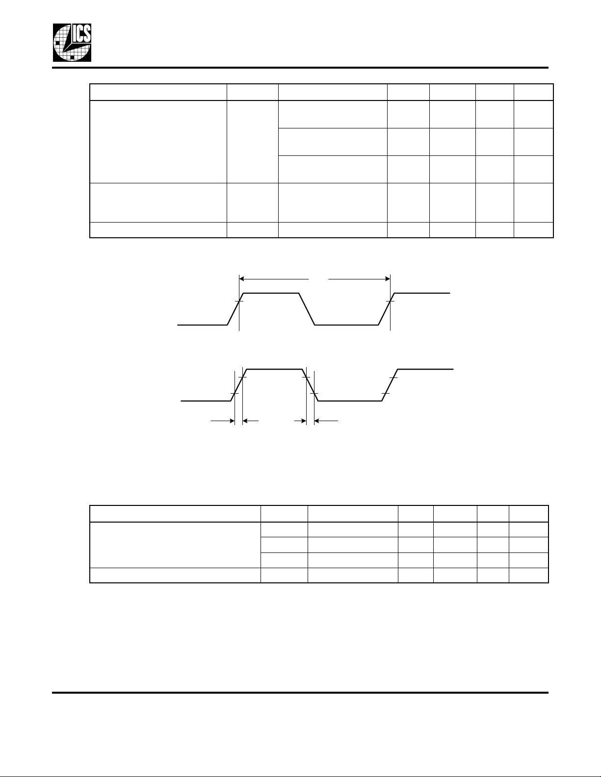
Spread Spectrum Profile
The ICS7151 low EMI clock generator uses a triangular
frequency modulation profile for optimal down stream
tracking of zero delay buffers and other PLL devices.
The frequency modulation amplitude is constant with
variations of the input frequency.
1) The 0.01µF decoupling capacitor should be mounted
on the component side of the board as close to the
VDD pin as possible. No vias should be used between
the decoupling capacitor and VDD pin. The PCB trace
to VDD pin should be kept as short as possible, as
should the PCB trace to the ground via.
2) To minimize EMI, the 27Ω series termination resistor
(if needed) should be placed close to the clock output.
3) An optimum layout is one with all components on the
same side of the board, minimizing vias through other
signal layers. Other signal traces should be routed
away from the ICS7151. This includes signal traces just
Modulation Rate
Frequency
Time
MDS 7151 E 3 Revision 012306
Integrated Circuit Systems, Inc. ● 525 Race Street, San Jose, CA 95126 ● tel (408) 297-1201 ● www.icst.com
Page 4

Absolute Maximum Ratings
Stresses above the ratings listed below can cause permanent damage to the ICS7151. These ratings,
which are standard values for ICS commercially rated parts, are stress ratings only. Functional operation of
the device at these or any other conditions above those indicated in the operational sections of the
specifications is not implied. Exposure to absolute maximum rating conditions for extended periods can
affect product reliability. Electrical parameters are guaranteed only over the recommended operating
temperature range.
Item Rating
Supply Voltage, VDD 7 V
All Inputs and Outputs (referenced to GND) -0.5 V to VDD+0.5 V
Ambient Operating Temperature -40 to +85°C
Storage Temperature -55 to +125°C
Junction Temperature -40 to +125°C
Soldering Temperature 260°C
Overshoot (V
Undershoot (V
) VDD + 1.0 V (t
IOVER
IUNDER
) GND - 1.0 V (t
ICS7151
Spread Spectrum Clock Generator
< 50 ns)
OVER
< 50 ns)
UNDER
Overshoot/Undershoot
V
< VDD + 1.0 V
IOVER
Input pin
t
< 50 ns
OVER
Recommended Operation Conditions
Parameter Min. Typ. Max. Units
Ambient Operating Temperature -40 +85 °C
Power Supply Voltage (measured in respect to GND) +3.0 3.3 3.6 V
V
IUNDER
t
< 50 ns
UNDER
< GND - 1.0 V
V
DD
GND
MDS 7151 E 4 Revision 012306
Integrated Circuit Systems, Inc. ● 525 Race Street, San Jose, CA 95126 ● tel (408) 297-1201 ● www.icst.com
Page 5

DC Electrical Characteristics
Unless stated otherwise, VDD = 3.3 V ±0.3 V, Ambient Temperature -40 to +85°C
Parameter Symbol Conditions Min. Typ. Max. Units
Operating Voltage VDD 3.0 3.3 3.6 V
Supply Current IDD No load, at 3.3 V 10 20 mA
Input High Voltage V
Input Low Voltage V
Output High Voltage V
Output Low Voltage V
Input Capacitance C
Load Capacitance C
Input Pull-up Resistor R
IH
IL
OH
OL
IN
L
PU
ICS7151
Spread Spectrum Clock Generator
XIN, S0, S1, ENS VDDx0.8 VDD + 0.3 V
XIN, S0, S1, ENS 0.0 VDDx0.20 V
CKOUT, IOH = -4 mA 2.0 V
CKOUT, IOL = 4 mA 0.4 V
XIN, S0, S1, ENS 16 pF
CKOUT, 8.3 to 66.7
15 pF
MHz
CKOUT, 66.7 to 100
10 pF
MHz
CKOUT, 100 to 133.4
7pF
MHz
ENS 100 240 400 kΩ
AC Electrical Characteristics
Unless stated otherwise, VDD = 3.3 V ±0.3 V, Ambient Temperature -40 to +85° C
Parameter Symbol Conditions Min. Typ. Max. Units
Input Crystal Frequency 16.5 33.4 MHz
Input Clock Frequency f
Output Frequency f
Input Clock Duty Cycle XIN, 16.5 to 33.4 MHz 40 50 60 %
Output Clock Duty Cycle t
Output Slew Rate CKOUT, 0.4 to 2.4 V,
IN
OUT
DCC
16.5 33.4 MHz
CKOUT, Multiply by 1
16.5 33.4 MHz
(ICS7151-10)
CKOUT, Multiply by 2
33.3 66.7 MHz
(ICS7151-20)
CKOUT, Multiply by 4
66.6 133.4 MHz
(ICS7151-40)
CKOUT, 2-frequency
8.3 16.7 MHz
division (ICS7151-50)
CKOUT, 1.5 V 40 60 %
0.5 3.0 V/ns
CL = 15 pF
MDS 7151 E 5 Revision 012306
Integrated Circuit Systems, Inc. ● 525 Race Street, San Jose, CA 95126 ● tel (408) 297-1201 ● www.icst.com
Page 6
Parameter Symbol Conditions Min. Typ. Max. Units
No load, spread off
(ICS7151-10, -20)
Cycle to Cycle Jitter t
JC
Power-up Time PLL lock-time from
Modulation Frequency f
MOD
No load, spread off
(ICS7151-40)
No load, spread off
(ICS7151-50)
power-up to 1% of final
value
CKOUT 33 kHz
ICS7151
Spread Spectrum Clock Generator
100 ps
150 ps
200 ps
25ms
Input Frequency (fIN = 1/tIN)
XIN
Output Slew Rate
CKOUT
t
r
SR = (2.4 - 0.4) /t
, SR = (2.4 - 0.4) /t
r
Thermal Characteristics 8 SOIC
Parameter Symbol Conditions Min. Typ. Max. Units
Thermal Resistance Junction to
Ambient
Thermal Resistance Junction to Case θ
t
IN
0.8 V
DD
2.4 V
0.4 V
t
f
f
θ
θ
θ
JA
JA
JA
JC
Still air 150 °C/W
1 m/s air flow 140 °C/W
3 m/s air flow 120 °C/W
40 °C/W
MDS 7151 E 6 Revision 012306
Integrated Circuit Systems, Inc. ● 525 Race Street, San Jose, CA 95126 ● tel (408) 297-1201 ● www.icst.com
Page 7

Spread Spectrum Clock Generator
Package Outline and Package Dimensions (8-pin SOIC, 150 Mil. Body)
Package dimensions are kept current with JEDEC Publication No. 95
ICS7151
INDEX
AREA
8
Symbol Min Max Min Max
Millimeters Inches
A 1.35 1.75 .0532 .0688
E
H
A1 0.10 0.25 .0040 .0098
B 0.330.51.013.020
C 0.19 0.25 .0075 .0098
D 4.80 5.00 .1890 .1968
E 3.80 4.00 .1497 .1574
1 2
e 1.27 BASIC 0.050 BASIC
H 5.80 6.20 .2284 .2440
D
h 0.250.50.010.020
L 0.401.27.016.050
α 0° 8° 0° 8°
A
A1
- C -
e
B
SEATING
.10 (.004)
PLANE
C
h x 45
C
L
MDS 7151 E 7 Revision 012306
Integrated Circuit Systems, Inc. ● 525 Race Street, San Jose, CA 95126 ● tel (408) 297-1201 ● www.icst.com
Page 8

ICS7151
Spread Spectrum Clock Generator
Ordering Information
Part / Order Number Marking Shipping Packaging Package Temperature
ICS7151M-10 7151M-10 Tubes 8-pin SOIC 0 to +70° C
ICS7151M-10T 7151M-10 Tape and Reel 8-pin SOIC 0 to +70
ICS7151M-10LF 7151M10L Tubes 8-pin SOIC 0 to +70
ICS7151M-10LFT 7151M10L Tape and Reel 8-pin SOIC 0 to +70
ICS7151M-20 7151M-20 Tubes 8-pin SOIC 0 to +70
ICS7151M-20T 7151M-20 Tape and Reel 8-pin SOIC 0 to +70
ICS7151M-20LF 7151M20L Tubes 8-pin SOIC 0 to +70
ICS7151M-20LFT 7151M20L Tape and Reel 8-pin SOIC 0 to +70
ICS7151M-40 7151M-40 Tubes 8-pin SOIC 0 to +70
ICS7151M-40T 7151M-40 Tape and Reel 8-pin SOIC 0 to +70
ICS7151M-40LF 7151M40L Tubes 8-pin SOIC 0 to +70
ICS7151M-40LFT 7151M40L Tape and Reel 8-pin SOIC 0 to +70
ICS7151M-50 7151M-50 Tubes 8-pin SOIC 0 to +70
ICS7151M-50T 7151M-50 Tape and Reel 8-pin SOIC 0 to +70
ICS7151M-50LF 7151M50L Tubes 8-pin SOIC 0 to +70
ICS7151M-50LFT 7151M50L Tape and Reel 8-pin SOIC 0 to +70
ICS7151MI-10 7151MI10 Tubes 8-pin SOIC -40 to +85
ICS7151MI-10T 7151MI10 Tape and Reel 8-pin SOIC -40 to +85
ICS7151MI-10LF 51MI10LF Tubes 8-pin SOIC -40 to +85
ICS7151MI-10LFT 51MI10LF Tape and Reel 8-pin SOIC -40 to +85
ICS7151MI-20 7151MI20 Tubes 8-pin SOIC -40 to +85
ICS7151MI-20T 7151MI20 Tape and Reel 8-pin SOIC -40 to +85
ICS7151MI-20LF 51MI20LF Tubes 8-pin SOIC -40 to +85
ICS7151MI-20LFT 51MI20LF Tape and Reel 8-pin SOIC -40 to +85
ICS7151MI-40 7151MI40 Tubes 8-pin SOIC -40 to +85
ICS7151MI-40T 7151MI40 Tape and Reel 8-pin SOIC -40 to +85
ICS7151MI-40LF 51MI40LF Tubes 8-pin SOIC -40 to +85
ICS7151MI-40LFT 51MI40LF Tape and Reel 8-pin SOIC -40 to +85
ICS7151MI-50 7151MI50 Tubes 8-pin SOIC -40 to +85
ICS7151MI-50T 7151MI50 Tape and Reel 8-pin SOIC -40 to +85
ICS7151MI-50LF 51MI50LF Tubes 8-pin SOIC -40 to +85
ICS7151MI-50LFT 51MI50LF Tape and Reel 8-pin SOIC -40 to +85
° C
° C
° C
° C
° C
° C
° C
° C
° C
° C
° C
° C
° C
° C
° C
° C
° C
° C
° C
° C
° C
° C
° C
° C
° C
° C
° C
° C
° C
° C
° C
Parts that are ordered with a “LF” suffix to the part number are the Pb-Free configuration and are RoHS compliant.
While the information presented herein has been checked for both accuracy and reliability, Integrated Circuit Systems (ICS)
assumes no responsibility for either its use or for the infringement of any patents or other rights of third parties, which would
result from its use. No other circuits, patents, or licenses are implied. This product is intended for use in normal commercial
applications. Any other applications such as those requiring extended temperature range, high reliability, or other extraordinary
environmental requirements are not recommended without additional processing by ICS. ICS reserves the right to change any
circuitry or specifications without notice. ICS does not authorize or warrant any ICS product for use in life support devices or
critical medical instruments.
MDS 7151 E 8 Revision 012306
Integrated Circuit Systems, Inc.
● 525 Race Street, San Jose, CA 95126 ● tel (408) 297-1201 ● www.icst.com
 Loading...