

Page 1
查询650R-27ILF供应商
ICS650-27
Networking Clock Source
Description
The ICS650-27 is a low cost, low jitter, high
performance clock synthesizer for networking
applications. Using analog Phase-Locked Loop (PLL)
techniques, the device accepts a 12.5 MHz or 25 MHz
clock or fundamental mode crystal input to produce
multiple output clocks for networking chips, PCI
devices, SDRAM, and ASICs. The ICS650-27 outputs
all have zero ppm synthesis error.
The ICS650-27 is pin compatible and functionally
equivalent to the ICS650-07. It is a performance
upgrade and is recommended for all new 3.3V
designs.
See the MK74CB214, ICS551, and ICS552-01 for
non-PLL buffer devices which produce multiple
low-skew copies of these output clocks.
See the ICS570, ICS9112-16/17/18 for zero delay
buffers that can synchronize outputs and other needed
clocks.
Features
• Packaged in 20-pin (150 mil) SSOP (QSOP)
• Available in Pb (lead) free package
• 12.5 MHz or 25 MHz fundamental crystal or clock
input
• Six output clocks with selectable frequencies
• SDRAM frequencies of 67, 83, 100, and 133 MHz
• Buffered crystal reference output
• Zero ppm synthesis error in all clocks
• Ideal for PMC-Sierra’s ATM switch chips
• Full CMOS output swing with 25 mA output drive
capability at TTL levels
• Advanced, low-power, sub-micron CMOS process
• Operating voltage of 3.3 V
• Industrial temperature only
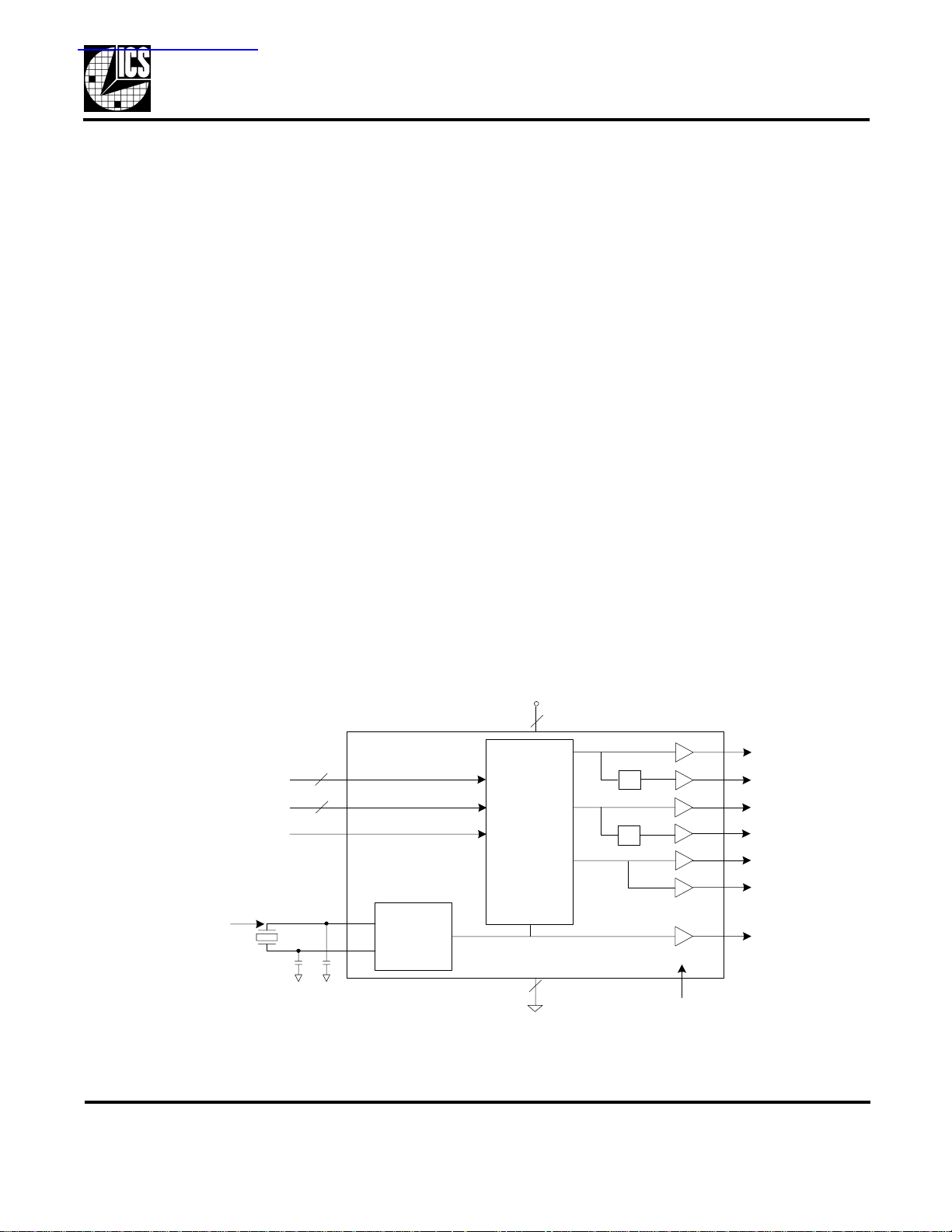
Block Diagram
25 or 12.5 MHz
cyrstal or clock
ACS1:0
BCS1:0
CCS
X1/ICLK
X2
VDD
2
CLKA1
2
2
Clock
Buffer/
Crystal
Oscillator
Clock
Synthesis
and Control
Circuitry
2
GND
/2
/2
OE (all outputs)
CLKA2
CLKB1
CLKB2
CLKC1
CLKC2
REFOUT
MDS 650-27 D 1 Revision 070505
Integrated Circuit Systems, Inc. ● 525 Race Street, San Jose, CA 95126 ● tel (408) 297-1201 ● www.icst.com
Page 2

Pin Assignment
ICS650-27
Networking Clock Source
1ASC0
X2 BCS0
VDD CLKA1
ASC1
GND
CLKC1
CLKC2
CLKB2 DC
CLKB1
2
3X1/ICLK
4
5
7
8
9
10
20-pin (150 mil) SSOP
Pin Descriptions
Pin
Number
1 ACS0 Input A clock select 0. Selects outputs on CLKA1 and CLKA2 per table on page 3.
2 X2 Input Crystal connection. Connect to a fundamental crystal or leave unconnected for a clock
Pin
Name
20 BCS1
19
18 REFOUT
17
16
156
14
13
12
11
Pin
Typ e
VDD
OE
GND
CLKA2
CCS
Pin Description
input.
3 X1/ICLK Input Crystal connection. Connect to a fundamental crystal or clock input.
4 VDD Power Connect to +3.3 V or 5 V. Must be the same as pin 16.
5 ACS1 Input A clock select 1. Selects outputs on CLKA1 and CLKA2 per table on page 3. Internal
pull-up.
6 GND Power Connect to ground.
7 CLKC1 Output Output Clock C1. Depends on setting of CCS per table on page 3.
8 CLKC2 Output Output Clock C2. Depends on setting of CCS per table on page 3. Same as CLKC1.
9 CLKB2 Output Output Clock B2. Depends on setting of BCS1, 0 per table on page 3.
10 CLKB1 Output Output Clock B1. Depends on setting of BCS1, 0 per table on page 3.
11 CCS Input Clock C select pin. Selects outputs on CLKC1 and CLKC2 per table on page 3.
12 DC - Don’t connect. Do not connect anything to this pin.
13 CLKA2 Output Output Clock A2. Depends on setting of ACS1, 0 per table on page 3.
14 GND Power Connect to ground.
15 OE Input Output enable. Tri-states all outputs when low. Internal pull-up.
16 VDD Power Connect to +3.3 V or 5 V. Must be the same as pin 4.
17 CLKA1 Output Output Clock A1. Depends on setting of ACS1, 0 per table on page 3.
18 REFOUT Output Buffered reference clock output. Same frequency as crystal or clock input.
19 BCS0 Input B clock select 0. Selects outputs on CLKB1 and CLKB2 per table on page 3.
20 BCS1 Input B clock select 1. Selects outputs on CLKB1 and CLKB2 per table on page 3. Internal
pull-up.
MDS 650-27 D 2 Revision 070505
Integrated Circuit Systems, Inc. ● 525 Race Street, San Jose, CA 95126 ● tel (408) 297-1201 ● www.icst.com
Page 3
Networking Clock Source
For a 25 MHz fundamental crystal or clock input, the following four tables apply:
ICS650-27
A Clocks Select Table (outputs in MHz)
ASC1 ASC0 CLKA1 CLKA2
00100off (low)
0 M Test Test
0175off (low)
1 0 33.3333 16.6667
1 M Test Test
1 1 66.6667 33.3333
C Clocks Select Table (outputs in MHz)
CCS CLKC1 CLKC2
0 125 125
M Test Test
17575
B Clocks Select Table (outputs in MHz)
BSC1 BSC0 CLKB1 CLKB2
0 0 Te s t Te st
0 M 66.6667 33.3333
0110050
1 0 83.3333 41.6667
1 M Te st Te s t
1 1 133.3333 66.6667
Reference Output Clock Frequency (in MHz)
REFOUT
25
For a 12.5 MHz fundamental crystal or clock input, the following four tables apply:
A Clocks Select Table (outputs in MHz)
B Clocks Select Table (outputs in MHz)
ASC1 ASC0 CLKA1 CLKA2
0050off (low)
0 M Test Test
0 1 37.5 off (low)
1 0 16.6667 8.3333
1 M Test Test
1 1 33.3333 16.6667
C Clocks Select Table (outputs in MHz)
CCS CLKC1 CLKC2
062.562.5
M Test Test
137.537.5
0 = connect directly to GND
M = leave unconnected (automatically self biases to VDD/2)
1 = connect directly to VDD
BSC1 BSC0 CLKB1 CLKB2
0 0 Te s t Te st
0 M 33.3333 16.6667
0 1 50 25
1 0 41.6667 20.8333
1 M Te st Te s t
1 1 66.6667 33.3333
Reference Output Clock Frequency (in MHz)
REFOUT
12.5
MDS 650-27 D 3 Revision 070505
Integrated Circuit Systems, Inc. ● 525 Race Street, San Jose, CA 95126 ● tel (408) 297-1201 ● www.icst.com
Page 4
ICS650-27
Networking Clock Source
External Components
The ICS650-27 requires a minimum number of external
components for proper operation.
Decoupling Capacitor
Decoupling capacitors of 0.01µF must be connected
between each VDD and GND (pins 4 and 6, pins 16
and 14), as close to the device as possible. For
optimum device performance, the decoupling capacitor
should be mounted on the component side of the PCB.
Avoid the use of vias in the decoupling circuit.
Series Termination Resistor
When the PCB trace between the clock outputs and the
loads are over 1 inch, series termination should be
used. To series terminate a 50Ω trace (a commonly
used trace impedance), place a 33Ω resistor in series
with the clock line as close to the clock output pin as
possible. The nominal impedance of the clock output is
20Ω.
Absolute Maximum Ratings
Crystal Information
The crystal used should be a fundamental mode (do
not use third overtone), parallel resonant. Crystal
capacitors should be connected from pins X1 to ground
and X2 to ground to optimize the initial accuracy. The
value of these capacitors is given by the following
equation:
Crystal caps (pF) = (C
In the equation, C
for a crystal with a 16pF load capacitance, two 20 pF
[(16-6) x 2] capacitors should be used.
is the crystal load capacitance. So,
L
- 6) x 2
L
Stresses above the ratings listed below can cause permanent damage to the ICS650-27. These ratings,
which are standard values for ICS commercially rated parts, are stress ratings only. Functional operation of
the device at these or any other conditions above those indicated in the operational sections of the
specifications is not implied. Exposure to absolute maximum rating conditions for extended periods can
affect product reliability. Electrical parameters are guaranteed only over the recommended operating
temperature range.
Item Rating
Supply Voltage, VDD 7 V
All Inputs and Outputs -0.5 V to VDD+0.5 V
Ambient Operating Temperature -40 to +85°C
Storage Temperature -65 to +150°C
Junction Temperature 175°C
Soldering Temperature 260°C
Recommended Operation Conditions
Parameter Min. Typ. Max. Units
Ambient Operating Temperature -40 +85 °C
Power Supply Voltage (measured in respect to GND) +3.0 +3.3 +3.6 V
MDS 650-27 D 4 Revision 070505
Integrated Circuit Systems, Inc. ● 525 Race Street, San Jose, CA 95126 ● tel (408) 297-1201 ● www.icst.com
Page 5
DC Electrical Characteristics
Unless stated otherwise, VDD = 3.3 V ±10%, Ambient Temperature -40 to +85°C
Parameter Symbol Conditions Min. Typ. Max. Units
Operating Voltage VDD 3.0 3.3 3.6 V
Input High Voltage V
Input Low Voltage V
Input High Voltage V
Input Low Voltage V
Input High Voltage V
Input Low Voltage V
Output High Voltage V
Output Low Voltage V
Output High Voltage, CMOS level V
Operating Supply Current I
Short Circuit Current I
Internal pull-up resistor R
Nominal output impedance Z
Networking Clock Source
X1 pin only, CLK input VDD/2+1 VDD/2 V
IH
X1 pin only, CLK input VDD/2 VDD/2-1 V
IL
all tri-level type inputs VDD-0.5 V
IH
all tri-level type inputs 0.5 V
IL
all other inputs 2 V
IH
all other inputs 0.8 V
IL
OHIOH
OL
OHIOH
DD
OS
PU
OUT
= -25 mA 2.4 V
IOL = 25mA 0.8 V
= -8 mA VDD-0.4 V
No Load 50 mA
Each output ±50 mA
BCS1, OE pins 510 kΩ
ACSI pin 120 kΩ
20 Ω
ICS650-27
AC Electrical Characteristics
Unless stated otherwise, VDD = 3.3 V±10%, Ambient Temperature -40 to +85°C
Parameter Symbol Conditions Min. Typ. Max. Units
Input Frequency 10 12.5 or 2527 MHz
Output Rise Time t
Output Fall Time t
Output Clock Duty Cycle At VDD/2, Note 1 40 50 60 %
Frequency Error All clocks 0 ppm
Absolute Jitter, short term Variation from mean,
Note 1: Measured with 15 pF load
Thermal Characteristics
Parameter Symbol Conditions Min. Typ. Max. Units
Thermal Resistance Junction to Ambient θ
Thermal Resistance Junction to Case θ
OR
OF
0.8 to 2.0 V, Note 1 1.5 ns
2.0 to 0.8 V, Note 1 1.5 ns
±150 ps
Note 1
Still air 135 °C/W
JA
θ
θ
1 m/s air flow 93 °C/W
JA
3 m/s air flow 78 °C/W
JA
JC
60 °C/W
MDS 650-27 D 5 Revision 070505
Integrated Circuit Systems, Inc. ● 525 Race Street, San Jose, CA 95126 ● tel (408) 297-1201 ● www.icst.com
Page 6
Networking Clock Source
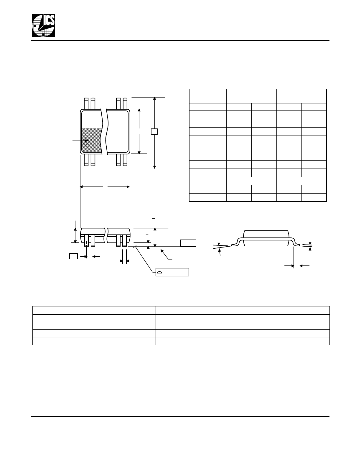
Package Outline and Package Dimensions (20-pin SSOP, 150 Mil. Body)
Package dimensions are kept current with JEDEC Publication No. 95
ICS650-27
INDEX
AREA
A2
20
Symbol Min Max Min Max
Millimeters Inches
A 1.351.75.053.069
A1 0.10 0.25 .0040 .010
E1
E
A2 -- 1.50 -- .059
b 0.20 0.30 0.008 0.012
C 0.180.25.007.010
D 8.558.75.337.344
E 5.806.20.228.244
1 2
E1 3.80 4.00 .150 .157
e 0.635 Basic 0.025 Basic
D
L 0.401.27.016.050
α 0° 8° 0° 8°
A
A1
- C -
e
b
SEATING
.10 (.004)
PLANE
C
L
c
Ordering Information
Part / Order Number Marking Shipping Packaging Package Temperature
ICS650R-27I ICS650R-27I Tubes 20-pin SSOP -40 to +85° C
ICS650R-27IT ICS650R-27I Tape and Reel 20-pin SSOP -40 to +85° C
ICS650R-27ILF 650R-27ILF Tubes 20-pin SSOP -40 to +85° C
ICS650R-27ILFT 650R-27ILF Tape and Reel 20-pin SSOP -40 to +85° C
Parts that are ordered with a "LF" suffix to the part number are the Pb-Free configuration and are RoHS compliant.
While the information presented herein has been checked for both accuracy and reliability, Integrated Circuit Systems (ICS)
assumes no responsibility for either its use or for the infringement of any patents or other rights of third parties, which would result
from its use. No other circuits, patents, or licenses are implied. This product is intended for use in normal commercial
applications. Any other applications such as those requiring extended temperature range, high reliability, or other extraordinary
environmental requirements are not recommended without additional processing by ICS. ICS reserves the right to change any
circuitry or specifications without notice. ICS does not authorize or warrant any ICS product for use in life support devices or
critical medical instruments.
MDS 650-27 D 6 Revision 070505
Integrated Circuit Systems, Inc. ● 525 Race Street, San Jose, CA 95126 ● tel (408) 297-1201 ● www.icst.com
 Loading...