

Page 1
Integrated Device Technology, Inc.
Document Type: Data Sheet
ICS1893CF
Document Stage: Rev. F Release
3.3-V 10Base-T/100Base-TX Integrated PHYceiver™
General
The ICS1893CF is a low-power, physical-layer device (PHY)
that supports the ISO/IEC 10Base-T and 100Base-TX
Carrier-Sense Multiple Access/Collision Detection
(CSMA/CD) Ethernet standards, ISO/IEC 8802-3.
The ICS1893CF is intended for MII, Node applications that
require the Auto-MDIX feature that automatically corrects
crossover errors in plant wiring.
The ICS1893CF incorporates Digital-Signal Processing (DSP)
control in its Physical-Medium Dependent (PMD) sub layer. As
a result, it can transmit and receive data on unshielded
twisted-pair (UTP) category 5 cables with attenuation in
excess of 24 dB at 100MHz. With this ICS-patented
technology, the ICS1893CF can virtually eliminate errors from
killer packets.
The ICS1893CF provides a Serial-Management Interface for
exchanging command and status information with a
Station-Management (STA) entity. The ICS1893CF
Media-Dependent Interface (MDI) can be configured to
provide either half- or full-duplex operation at data rates of 10
Mb/s or 100Mb/s.
The ICS1893CF is available in a 300-mil 48-lead SSOP
package. The ICS1893CF shares the same proven
performance circuitry with the ICS1893BF and is a pin-for-pin
replacement of the 1893BF.
Applications: NIC cards, PC motherboards, switches,
routers, DSL and cable modems, game machines, printers,
network connected appliances, and industrial equipment.
Features
• Supports category 5 cables with attenuation in excess of
24dB at 100 MHz.
• Single-chip, fully integrated PHY provides PCS, PMA, PMD,
and AUTONEG sub layers functions of IEEE standard.
• 10Base-T and 100Base-TX IEEE 8802.3 compliant
• Single 3.3V power supply
• Highly configurable, supports:
– Media Independent Interface (MII)
– Auto-Negotiation with Parallel detection
– Node applications, managed or unmanaged
– 10M or 100M full and half-duplex modes
– Loopback mode for Diagnostic Functions
– Auto-MDI/MDIX crossover correction
• Low-power CMOS (typically 400 mW)
• Power-Down mode typically 21mW
• Clock and crystal supported
• Fully integrated, DSP-based PMD includes:
– Adaptive equalization and baseline-wander correction
– Transmit wave shaping and stream cipher scrambler
– MLT-3 encoder and NRZ/NRZI encoder
• Small footprint 48-pin 300 mil. SSOP package
• Also available in small footprint 56-pin 8x8 MLF2 package
• Available in Industrial Temp and Lead Free
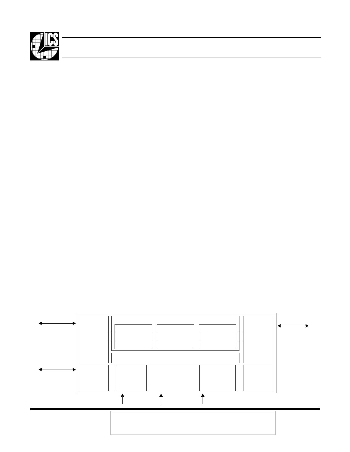
ICS1893CF Block Diagram
100Base-T
PCS
10/100 MII
MAC
Interface
MII
Management
Interface
Interface
MUX
MII
Extended
Register
Set
ICS1893CF, Rev. F, 03/01/07 Mar. 2007
• Framer
• CRS/COL
Detection
• Parallel to Serial
•4B/5B
Low-Jitter
Clock
Synthesizer
Clock Power LEDs and PHY
IDT reserves the right to make changes in the device data identified in
PMA
• Clock Recovery
• Link Monitor
• Signal Detection
• Error Detection
10Base-T
this publication without further notice. IDT advises its customers to
obtain the latest version of all device data to verify that any information
being relied upon by the customer is current and accurate.
TP_PMD
•MLT-3
• Stream Cipher
• Adaptive Equalizer
• Baseline Wander
Correction
Configuration
and Status
Address
Integrated
Switch
Auto-
Negotiation
Twi ste d-
Pair
Interface to
Magnetics
Modules and
RJ45
Connector
Page 2

Revision History
• Initial preliminary release of this document, Rev A, dated July 10, 2006.
• Rev B – remove all references to ICS1893CK; removed package drawing and ordering info.
• Rev C – added CK package and ordering information back to datasheet; removed TOC.
• Rev E – changed resistor values in table 9.3 and on Figure 9-1, “ICS1893CF 10TCSR and 100TCSR”.
Revision HistoryICS1893CF Data Sheet - Release
ICS1893CF, Rev. F, 03/01/07 Mar. 2007
Copyright © 2007, Integrated Device Technology, Inc.
All rights reserved.
2
Page 3

ICS1893CF Data Sheet Rev. F - Release
Chapter 1 Abbreviations and Acronyms
Chapter 1 Abbreviations and Acronyms
Table 1-1 lists and interprets the abbreviations and acronyms used throughout this data sheet.
Table 1-1. Abbreviations and Acronyms
Abbreviation /
Acronym
4B/5B 4-Bit / 5-Bit Encoding/Decoding
ANSI American National Standards Institute
CMOS complimentary metal-oxide semiconductor
CSMA/CD Carrier Sense Multiple Access with Collision Detection
CW Command Override Write
DSP digital signal processing
ESD End-of-Stream Delimiter
FDDI Fiber Distributed Data Interface
FLL frequency-locked loop
FLP Fast Link Pulse
IDL A ‘dead’ time on the link following a 10Base-T packet, not to be confused with idle
IEC International Electrotechnical Commission
IEEE Institute of Electrical and Electronic Engineers
ISO International Standards Organization
LH Latching High
LL Latching Low
LMX Latching Maximum
MAC Media Access Control
Interpretation
Max. maximum
Mbps Megabits per second
MDI Media Dependent Interface
MDIX Media Independent Interface Crossed
MF Management Frame
MII Media Independent Interface
Min. minimum
MLT-3 Multi-Level Transition Encoding (3 Levels)
N/A Not Applicable
NLP Normal Link Pulse
No. Number
NRZ Not Return to Zero
NRZI Not Return to Zero, Invert on one
ICS1893CF, Rev. F, 03/01/07 Mar. 2007
Copyright © 2007, Integrated Device Technology, Inc.
All rights reserved.
3
Page 4

Table 1-1. Abbreviations and Acronyms (Continued)
Chapter 1 Abbreviations and AcronymsICS1893CF Data Sheet - Release
Abbreviation /
Acronym
OSI Open Systems Interconnection
OUI Organizationally Unique Identifier
PCS Physical Coding sublayer
PHY physical-layer device
The ICS1893CF is a physical-layer device, also referred to as a ‘PHY’ or ‘PHYceiver’.
(The ICS1890 is also a physical-layer device.)
PLL phase-locked loop
PMA Physical Medium Attachment
PMD Physical Medium Dependent
ppm parts per million
RO read only
R/W read/write
R/W0 read/write zero
SC self-clearing
SF Special Functions
SFD Start-of-Frame Delimiter
Interpretation
SI Stream Interface, Serial Interface, or Symbol Interface.
With reference to the MII/SI pin, the acronym ‘SI’ has multiple meanings.
• Generically, SI means 'Stream Interface', and is documented as such in this data
sheet.
• However, when the MAC Interface is configured for:
– 10M operations, SI is an acronym for 'Serial Interface'.
– 100M operations, SI is an acronym for 'Symbol Interface'.
SQE Signal Quality Error
SSD Start-of-Stream Delimiter
SSOP Small Shrink Outline Package
STA Station Management Entity
STP shielded twisted pair
TAF Technology Ability Field
TP-PMD Twisted-Pair Physical Layer Medium Dependent
Typ. typical
UTP unshielded twisted pair
ICS1893CF, Rev. F, 03/01/07 Mar. 2007
Copyright © 2007, Integrated Device Technology, Inc.
All rights reserved.
4
Page 5

ICS1893CF Data Sheet Rev. F - Release
Chapter 2 Conventions and Nomenclature
Chapter 2 Conventions and Nomenclature
Table 2-1 lists and explains the conventions and nomenclature used throughout this data sheet.
Table 2-1. Conventions and Nomenclature
Item Convention / Nomenclature
Bits
Code groups Within this table, see the item ‘Symbols’
Colon (:) Within this table, see these items:
Numbers
Pin (or signal) names
• A bit in a register is identified using the format ‘register.bit’. For example, bit
0.15 is bit 15 of register 0.
• When a colon is used with bits, it indicates the range of bits. For example,
bits 1.15:11 are bits 15, 14, 13, 12, and 11 of register 1.
• For a range of bits, the order is always from the most-significant bit to the
least-significant bit.
• ‘Bits’
• ‘Pin (or signal) names’
• As a default, all numbers use the decimal system (that is, base 10) unless
followed by a lowercase letter. A string of numbers followed by a lowercase
letter:
– A ‘b’ represents a binary (base 2) number
– An ‘h’ represents a hexadecimal (base 16) number
– An ‘o’ represents an octal (base 8) number
• All numerical references to registers use decimal notation (and not
hexadecimal).
• All pin or signal names are provided in capital letters.
• A pin name that includes a forward slash ‘/’ is a multi-function, configuration
pin. These pins provide the ability to select between two ICS1893CF
functions. The name provided:
– Before the ‘/’ indicates the pin name and function when the signal level
on the pin is logic zero.
– After the ‘/’ indicates the pin name and function when the signal level on
the pin is logic one.
For example, the HW/SW pin selects between Hardware (HW) mode and
Software (SW) mode. When the signal level on the HW/SW pin is logic:
– Zero, the ICS1893CF Hardware mode is selected.
– One, the ICS1893CF Software mode is selected.
• An ‘n’ appended to the end of a pin name or signal name (such as
RESETn) indicates an active-low operation.
• When a colon is used with pin or signal names, it indicates a range. For
example, TXD[3:0] represents pins/signals TXD3, TXD2, TXD1, and TXD0.
• When pin name abbreviations are spelled out, words in parentheses
indicate additional description that is not part of the pin name abbreviation.
Registers
• A bit in a register is identified using the format ‘register.bit’. For example, bit
0.15 is bit 15 of register 0.
• All numerical references to registers use decimal notation (and not
hexadecimal).
• When register name abbreviations are spelled out, words in parentheses
indicate additional description that is not part of the register name
abbreviation.
ICS1893CF, Rev. F, 03/01/07 Mar. 2007
Copyright © 2007, Integrated Device Technology, Inc.
All rights reserved.
5
Page 6

Table 2-1. Conventions and Nomenclature (Continued)
Item Convention / Nomenclature
Signal references • When referring to signals, the terms:
– ‘FALSE’, ‘low’, or ‘zero’ represent signals that are logic zero.
– ‘TRUE’, ‘high’, or ‘one’ represent signals that are logic one.
• Chapter 9, “DC and AC Operating Conditions” defines the electrical
specifications for ‘logic zero’ and ‘logic one’ signals.
Symbols
• In this data sheet, code group names are referred to as ‘symbols’ and they
are shown between '/' (slashes). For example, the symbol /J/ represents
the first half of the Start-of-Stream Delimiter (SSD1).
• Symbol sequences are shown in succession. For example, /I/J/K/
represents an IDLE followed by the SSD.
Chapter 2 Conventions and NomenclatureICS1893CF Data Sheet - Release
Terms:
‘set’,
‘active’,
‘asserted’,
Terms:
‘cleared’,
‘de-asserted’,
‘inactive’
Terms:
‘twisted-pair receiver’
Terms:
‘twisted-pair transmitter’
The terms ‘set’, ‘active’, and ‘asserted’ are synonymous.
They do not necessarily infer logic one.
(For example, an active-low signal can be set to logic zero.)
The terms ‘cleared’, ‘inactive’, and ‘de-asserted’ are synonymous.
They do not necessarily infer logic zero.
In reference to the ICS1893CF, the term ‘Twisted-Pair Receiver’ refers to the
set of Twisted-Pair Receive output pins (TP_RXP and TP_RXN).
In reference to the ICS1893CF, the term ‘Twisted-Pair Transmitter’ refers to
the set of Twisted-Pair Transmit output pins (TP_TXP and TP_TXN).
ICS1893CF, Rev. F, 03/01/07 Mar. 2007
Copyright © 2007, Integrated Device Technology, Inc.
All rights reserved.
6
Page 7

ICS1893CF Data Sheet Rev. F - Release
Chapter 3 Overview of the ICS1893CF
The ICS1893CF is a stream processor. During data transmission, it accepts sequential nibbles from its
MAC (Media Access Control) converts them into a serial bit stream, encodes them, and transmits them
over the medium through an external isolation transformer. When receiving data, the ICS1893CF converts
and decodes a serial bit stream (acquired from an isolation transformer that interfaces with the medium)
into sequential nibbles. It subsequently presents these nibbles to its MAC Interface.
The ICS1893CF implements the OSI model’s physical layer, consisting of the following, as defined by the
ISO/IEC 8802-3 standard:
• Physical Coding sublayer (PCS)
• Physical Medium Attachment sublayer (PMA)
• Physical Medium Dependent sublayer (PMD)
• Auto-Negotiation sublayer
The ICS1893CF is transparent to the next layer of the OSI model, the link layer. The link layer has two
sublayers: the Logical Link Control sublayer and the MAC sublayer. The ICS1893CF can interface directly
to the MAC.
The ICS1893CF transmits framed packets acquired from its MAC Interface and receives encapsulated
packets from another PHY, which it translates and presents to its MAC Interface.
Chapter 3 Overview of the ICS1893CF
Note: As per the ISO/IEC standard, the ICS1893CF does not affect, nor is it affected by, the underlying
structure of the MAC frame it is conveying.
ICS1893CF, Rev. F, 03/01/07 Mar. 2007
Copyright © 2007, Integrated Device Technology, Inc.
All rights reserved.
7
Page 8

3.1 100Base-TX Operation
During 100Base-TX data transmission, the ICS1893CF accepts packets from a MAC and inserts
Start-of-Stream Delimiters (SSDs) and End-of-Stream Delimiters (ESDs) into the data stream. The
ICS1893CF encapsulates each MAC frame, including the preamble, with an SSD and an ESD. As per the
ISO/IEC Standard, the ICS1893CF replaces the first octet of each MAC preamble with an SSD and
appends an ESD to the end of each MAC frame.
When receiving data from the medium, the ICS1893CF removes each SSD and replaces it with the
pre-defined preamble pattern before presenting the nibbles to its MAC Interface. When the ICS1893CF
encounters an ESD in the received data stream, signifying the end of the frame, it ends the presentation of
nibbles to its MAC Interface. Therefore, the local MAC receives an unaltered copy of the transmitted frame
sent by the remote MAC.
During periods when MAC frames are being neither transmitted nor received, the ICS1893CF signals and
detects the IDLE condition on the Link Segment. In the 100Base-TX mode, the ICS1893CF transmit
channel sends a continuous stream of scrambled ones to signify the IDLE condition. Similarly, the
ICS1893CF receive channel continually monitors its data stream and looks for a pattern of scrambled ones.
The results of this signaling and monitoring provide the ICS1893CF with the means to establish the
integrity of the Link Segment between itself and its remote link partner and inform its Station Management
Entity (STA) of the link status.
For 100M data transmission, the ICS1893CF MAC Interface is configured to provide a 100M Media
Independent Interface (MII).
Chapter 3 Overview of the ICS1893CFICS1893CF Data Sheet - Release
3.2 10Base-T Operation
During 10Base-T data transmission, the ICS1893CF inserts only the IDL delimiter into the data stream. The
ICS1893CF appends the IDL delimiter to the end of each MAC frame. However, since the 10Base-T
preamble already has a Start-of-Frame delimiter (SFD), it is not required that the ICS1893CF insert an
SSD-like delimiter.
When receiving data from the medium (such as a twisted-pair cable), the ICS1893CF uses the preamble to
synchronize its receive clock. When the ICS1893CF receive clock establishes lock, it presents the
preamble nibbles to its MAC Interface. The 10M MAC Interface uses the standard MII Interface.
In 10M operations, during periods when MAC frames are being neither transmitted nor received, the
ICS1893CF signals and detects Normal Link Pulses. This action allows the integrity of the Link Segment
with the remote link partner to be established and then reported to the ICS1893CF’s STA.
ICS1893CF, Rev. F, 03/01/07 Mar. 2007
Copyright © 2007, Integrated Device Technology, Inc.
All rights reserved.
8
Page 9

ICS1893CF Data Sheet Rev. F - Release
Chapter 4 Operating Modes Overview
The ICS1893CF operating modes are typically controlled from software.
The ICS1893CF register bits are accessible through a standard MII (Media Independent Interface) Serial
Management Port.
The ICS1893CF is configured to support the MAC Interface as a 10M MII or a 100M MII. The protocol on
the Medium Dependent Interface (MDI) can be configured to support either 10M or 100M operations in
either half-duplex or full-duplex modes.
The ICS1893CF is fully compliant with the ISO/IEC 8802-3 standard, as it pertains to both 10Base-T and
100Base-TX operations. The feature-rich ICS1893CF allows easy migration from 10-Mbps to 100-Mbps
operations as well as from systems that require support of both 10M and 100M links.
This chapter is an overview of the following ICS1893CF modes of operation:
• Section 4.1, “Reset Operations”
• Section 4.2, “Power-Down Operations”
• Section 4.3, “Automatic Power-Saving Operations”
• Section 4.4, “Auto-Negotiation Operations”
• Section 4.5, “100Base-TX Operations”
• Section 4.6, “10Base-T Operations”
• Section 4.7, “Half-Duplex and Full-Duplex Operations”
• Section 4.8, “Auto-MDI/MDIX Crossover”
Chapter 4 Operating Modes Overview
ICS1893CF, Rev. F, 03/01/07 Mar. 2007
Copyright © 2007, Integrated Device Technology, Inc.
All rights reserved.
9
Page 10

4.1 Reset Operations
This section first discusses reset operations in general and then specific ways in which the ICS1893CF can
be configured for various reset options.
4.1.1 General Reset Operations
The following reset operations apply to all the specific ways in which the ICS1893CF can be reset, which
are discussed in Section 4.1.2, “Specific Reset Operations”.
4.1.1.1 Entering Reset
When the ICS1893CF enters a reset condition (either through hardware, power-on reset, or software), it
does the following:
1. Isolates the MAC Interface input pins
2. Drives all MAC Interface output pins low
3. Tri-states the signals on its Twisted-Pair Transmit pins (TP_TXP and TP_TXN)
4. Initializes all its internal modules and state machines to their default states
5. Enters the power-down state
6. Initializes all internal latching low (LL), latching high (LH), and latching maximum (LMX) Management
Register bits to their default values
Chapter 4 Operating Modes OverviewICS1893CF Data Sheet - Release
4.1.1.2 Exiting Reset
When the ICS1893CF exits a reset condition, it does the following:
1. Exits the power-down state
2. Latches the Serial Management Port Address of the ICS1893CF into the Extended Control Register,
bits 16.10:6. [See Section 7.11.3, “PHY Address (bits 16.10:6)”.]
3. Enables all its internal modules and state machines
4. Sets all Management Register bits to their default values
5. Enables the Twisted-Pair Transmit pins (TP_TXP and TP_TXN)
6. Resynchronizes both its Transmit and Receive Phase-Locked Loops, which provide its transmit clock
(TXCLK) and receive clock (RXCLK)
7. Releases all MAC Interface pins, which takes a maximum of 640 ns after the reset condition is removed
4.1.1.3 Hot Insertion
As with the ICS189X products, the ICS1893CF reset design supports ‘hot insertion’ of its MII. (That is, the
ICS1893CF can connect its MAC Interface to a MAC while power is already applied to the MAC.)
ICS1893CF, Rev. F, 03/01/07 Mar. 2007
Copyright © 2007, Integrated Device Technology, Inc.
All rights reserved.
10
Page 11

ICS1893CF Data Sheet Rev. F - Release
4.1.2 Specific Reset Operations
This section discusses the following specific ways that the ICS1893CF can be reset:
• Hardware reset (using the RESETn pin)
• Power-on reset (applying power to the ICS1893CF)
• Software reset (using Control Register bit 0.15)
Note: At the completion of a reset (either hardware, power-on, or software), the ICS1893CF sets all
registers to their default values.
4.1.2.1 Hardware Reset
Entering Hardware Reset
Holding the active-low RESETn pin low for a minimum of five REF_IN clock cycles initiates a hardware
reset (that is, the ICS1893CF enters the reset state). During reset, the ICS1893CF executes the steps
listed in Section 4.1.1.1, “Entering Reset”.
Exiting Hardware Reset
After the signal on the RESETn pin transitions from a low to a high state, the ICS1893CF completes in 640
ns (that is, in 16 REF_IN clocks) steps 1 through 5, listed in Section 4.1.1.2, “Exiting Reset”. After the first
five steps are completed, the Serial Management Port is ready for normal operations, but this action does
not signify the end of the reset cycle. The reset cycle completes when the transmit clock (TXCLK) and
receive clock (RXCLK) are available, which is typically 53 ms after the RESETn pin goes high. [For details
on this transition, see Section 9.5.16, “Reset: Hardware Reset and Power-Down”.]
Chapter 4 Operating Modes Overview
Note:
1. The MAC Interface is not available for use until the TXCLK and RXCLK are valid.
2. The Control Register bit 0.15 does not represent the status of a hardware reset. It is a self-clearing bit
that is used to initiate a software reset.
4.1.2.2 Power-On Reset
Entering Power-On Reset
When power is applied to the ICS1893CF, it waits until the potential between VDD and VSS achieves a
minimum voltage before entering reset and executing the steps listed in Section 4.1.1.1, “Entering Reset”.
After entering reset from a power-on condition, the ICS1893CF remains in reset for approximately 20 µs.
(For details on this transition, see Section 9.5.15, “Reset: Power-On Reset”.)
Exiting Power-On Reset
The ICS1893CF automatically exits reset and performs the same steps as for a hardware reset. (See
Section 4.1.1.2, “Exiting Reset”.)
Note: The only difference between a hardware reset and a power-on reset is that during a power-on
reset, the ICS1893CF isolates its RESETn input pin. All other functionality is the same. As with a
hardware reset, Control Register bit 0.15 does not represent the status of a power-on reset.
ICS1893CF, Rev. F, 03/01/07 Mar. 2007
Copyright © 2007, Integrated Device Technology, Inc.
All rights reserved.
11
Page 12

4.1.2.3 Software Reset
Entering Software Reset
Initiation of a software reset occurs when a management entity writes a logic one to Control Register bit
0.15. When this write occurs, the ICS1893CF enters the reset state for two REF_IN clock cycles.
Note: Entering a software reset is nearly identical to entering a hardware reset or a power-on reset,
except that during a software-initiated reset, the ICS1893CF does not enter the power-down state.
Exiting Software Reset
At the completion of a reset (either hardware, power-on, or software), the ICS1893CF sets all registers to
their default values. This action automatically clears (that is, sets equal to logic zero) Control Register bit
0.15, the software reset bit. Therefore, for a software reset (only), bit 0.15 is a self-clearing bit that indicates
the completion of the reset process.
Note:
1. The RESETn pin is active low but Control Register bit 0.15 is active high.
2. Exiting a software reset is nearly identical to exiting a hardware reset or a power-on reset, except that
upon exiting a software-initiated reset, the ICS1893CF does not re-latch its Serial Management Port
Address into the Extended Control Register. [For information on the Serial Management Port Address,
see Section 7.11.3, “PHY Address (bits 16.10:6)”.]
3. The Control Register bit 0.15 does not represent the status of a hardware reset. It is a self-clearing bit
that is used to initiate a software reset. During a hardware or power-on reset, Control Register bit 0.15
does not get set to logic one. As a result, this bit 0.15 cannot be used to indicate the completion of the
reset process for hardware or power-on resets.
Chapter 4 Operating Modes OverviewICS1893CF Data Sheet - Release
4.2 Power-Down Operations
The ICS1893CF enters the power-down state whenever either (1) the RESETn pin is low or (2) Control
Register bit 0.11 (the Power-Down bit) is logic one. In the power-down state, the ICS1893CF disables all
internal functions and drives all MAC Interface output pins to logic zero except for those that support the MII
Serial Management Port. In addition, the ICS1893CF tri-states its Twisted-Pair Transmit pins (TP_TXP and
TP_TXN) to achieve an additional reduction in power.
There is one significant difference between entering the power-down state by setting Control Register bit
0.11 as opposed to entering the power-down state during a reset. When the ICS1893CF enters the
power-down state:
• By setting Control Register bit 0.11, the ICS1893CF maintains the value of all Management Register bits
except for the latching low (LL), latching high (LH), and latching maximum (LMX) status bits. Instead,
these LL, LH, and LMX Management Register bits are re-initialized to their default values.
• During a reset, the ICS1893CF sets all of its Management Register bits to their default values. It does not
maintain the state of any Management Register bit.
For more information on power-down operations, see the following:
• Section 7.14, “Register 19: Extended Control Register 2”
• Section 9.4, “DC Operating Characteristics”, which has tables that specify the ICS1893CF power
consumption while in the power-down state
ICS1893CF, Rev. F, 03/01/07 Mar. 2007
Copyright © 2007, Integrated Device Technology, Inc.
All rights reserved.
12
Page 13

ICS1893CF Data Sheet Rev. F - Release
4.3 Automatic Power-Saving Operations
The ICS1893CF has power-saving features that automatically minimize its total power consumption while it
is operating. Table 4-1 lists the ICS1893CF automatic power-saving features for the various modes.
Table 4-1. Automatic Power-Saving Features, 10Base-T and 100Base-TX Modes
Chapter 4 Operating Modes Overview
PowerSaving
Feature
Disable Internal Modules
STA Control
of Automatic
PowerSaving
Features
In 10Base-T mode, the ICS1893CF
disables all its internal 100Base-TX
modules.
When an STA sets the state of the
ICS1893CF Extended Control Register 2,
bit 19.0 to logic:
• Zero, the 100Base-TX modules always
remain enabled, even during 10Base-T
operations.
10Base-T Mode 100Base-TX Mode
• One, the ICS1893CF automatically
disables 100Base-TX modules while the
ICS1893CF is operating in 10Base-T
mode.
4.4 Auto-Negotiation Operations
The ICS1893CF has an Auto-Negotiation sublayer and provides a Control Register bit (bit 0.12) to
determine whether its Auto-Negotiation sublayer is enabled or disabled.
When enabled, the ICS1893CF Auto-Negotiation sublayer exchanges technology capability data with its
remote link partner and automatically selects the highest-performance operating mode it has in common
with its remote link partner. For example, if the ICS1893CF supports 100Base-TX and 10Base-T modes –
but its link partner supports 100Base-TX and 100Base-T4 modes – the two devices automatically select
100Base-TX as the highest-performance common operating mode. For details regarding initialization and
control of the auto-negotiation process, see Section 6.2, “Functional Block: Auto-Negotiation”.
Mode for ICS1893CF
In 100Base-TX mode, the ICS1893CF
disables all its internal 10Base-T modules.
When an STA sets the state of the
ICS1893CF Extended Control Register 2,
bit 19.1 to logic:
• Zero, the 10Base-T modules always
remain enabled, even during
100Base-TX operations.
• One, the ICS1893CF automatically
disables 10Base-T modules while the
ICS1893CF is operating in 100Base-TX
mode.
ICS1893CF, Rev. F, 03/01/07 Mar. 2007
Copyright © 2007, Integrated Device Technology, Inc.
All rights reserved.
13
Page 14

4.5 100Base-TX Operations
The ICS1893CF 100Base-TX mode provides 100Base-TX physical layer (PHY) services as defined in the
ISO/IEC 8802-3 standard. In the 100Base-TX mode, the ICS1893CF is a 100M translator between a MAC
and the physical transmission medium. As such, the ICS1893CF has two interfaces, both of which are fully
configurable: one to the MAC and one to the Link Segment. In 100Base-TX mode, the ICS1893CF
provides the following functions:
• Data conversion from both parallel-to-serial and serial-to-parallel formats
• Data encoding/decoding (4B/5B, NRZ/NRZI, and MLT-3)
• Data scrambling/descrambling
• Data transmission/reception over a twisted-pair medium
To accurately transmit and receive data, the ICS1893CF employs DSP-based wave shaping, adaptive
equalization, and baseline wander correction. In addition, in 100Base-TX mode, the ICS1893CF provides
a variety of control and status means to assist with Link Segment management. For more information on
100Base-TX, see Section 6.4, “Functional Block: 100Base-TX TP-PMD Operations”.
4.6 10Base-T Operations
The ICS1893CF 10Base-T mode provides 10Base-T physical layer (PHY) services as defined in the
ISO/IEC 8802-3 standard. In the 10Base-T mode, the ICS1893CF is a 10M translator between a MAC and
the physical transmission medium. In 10Base-T mode, the ICS1893CF provides the following functions:
• Data conversion from both parallel-to-serial and serial-to-parallel formats
• Manchester data encoding/decoding
• Data transmission/reception over a twisted-pair medium
Chapter 4 Operating Modes OverviewICS1893CF Data Sheet - Release
4.7 Half-Duplex and Full-Duplex Operations
The ICS1893CF supports half-duplex and full-duplex operations for both 10Base-T and 100Base-TX
applications. Full-duplex operation allows simultaneous transmission and reception of data, which
effectively doubles the Link Segment throughput to either 20 Mbps (for 10Base-T operations) or 200 Mbps
(for 100Base-TX operations).
As per the ISO/IEC standard, full-duplex operations differ slightly from half-duplex operations. These
differences are necessary, as during full-duplex operations a PHY actively uses both its transmit and
receive data paths simultaneously.
• In 10Base-T full-duplex operations, the ICS1893CF disables its loopback function (that is, it does not
automatically loop back data from its transmitter to its receiver) and disables its SQE Test function.
• In both 10Base-T and 100Base-TX full-duplex operations, the ICS1893CF asserts its CRS signal only in
response to receive activity while its COL signal always remains inactive.
For more information on half-duplex and full-duplex operations, see the following sections:
• Section 7.2, “Register 0: Control Register”
• Section 7.2.8, “Duplex Mode (bit 0.8)”
• Section 7.3, “Register 1: Status Register”
• Section 7.6, “Register 4: Auto-Negotiation Register”
ICS1893CF, Rev. F, 03/01/07 Mar. 2007
Copyright © 2007, Integrated Device Technology, Inc.
All rights reserved.
14
Page 15

ICS1893CF Data Sheet Rev. F - Release
4.8 Auto-MDI/MDIX Crossover (New)
The ICS1893CF includes the auto-MDI/MDIX crossover feature. In a typical CAT 5 Ethernet installation the
transmit twisted pair signal pins of the RJ45 connector are crossed over in the CAT 5 wiring to the partners
receive twisted pair signal pins and receive twisted pair to the partners transmit twisted pair. This is usually
accomplished in the wiring plant. Hubs generally wire the RJ45 connector crossed to accomplish the
crossover. Two types of CAT 5 cables (straight and crossed) are available to achieve the correct
connection. The Auto-MDI/MDIX feature automatically corrects for miss-wired installations by automatically
swapping transmit and receive signal pairs at the PHY when no link results. Auto-MDI/MDIX is automatic,
but may be disabled for test purposes using the AMDIX_EN pin or by writing MDIO register 19 Bits 9:8 in
the MDIO register. The Auto-MDI/MDIX function is independent of Auto-Negotiation and preceeds
Auto-Negotiation when enabled.
Chapter 4 Operating Modes Overview
ICS1893CF, Rev. F, 03/01/07 Mar. 2007
Copyright © 2007, Integrated Device Technology, Inc.
All rights reserved.
15
Page 16

Chapter 5 Interface Overviews
The ICS1893CF MAC Interface is fully configurable, thereby allowing it to accommodate many different
applications.
This chapter includes overviews of the following MAC-to-PHY interfaces:
• Section 5.1, “MII Data Interface”
• Section 5.2, “Serial Management Interface”
• Section 5.3, “Twisted-Pair Interface”
• Section 5.4, “Clock Reference Interface”
• Section 5.5, “Status Interface”
Chapter 5 Interface OverviewsICS1893CF Data Sheet - Release
ICS1893CF, Rev. F, 03/01/07 Mar. 2007
Copyright © 2007, Integrated Device Technology, Inc.
All rights reserved.
16
Page 17

ICS1893CF Data Sheet Rev. F - Release
5.1 MII Data Interface
The ICS1893CF’s MAC Interface is the Media Independent Interface (MII) operating at either 10 Mbps or
100 Mbps. The ICS1893CF MAC Interface is configured for the MII Data Interface mode, data is transferred
between the PHY and the MAC as framed, 4-bit parallel nibbles. In addition, the interface also provides
status and control signals to synchronize the transfers.
The ICS1893CF provides a full complement of the ISO/IEC-specified MII signals. Its MII has both a
transmit and a receive data path to synchronously exchange 4 bits of data (that is, nibbles).
• The ICS1893CF’s MII transmit data path includes the following:
– A data nibble, TXD[3:0]
– A transmit data clock to synchronize transfers, TXCLK
– A transmit enable signal, TXEN
– The TXER pin is not available on the ICS1893CF
• The ICS1893CF’s MII receive data path includes the following:
– A separate data nibble, RXD[3:0]
– A receive data clock to synchronize transfers, RXCLK
– A receive data valid signal, RXDV
Both the MII transmit clock and the MII receive clock are provided to the MAC/Reconciliation sublayer by
the ICS1893CF (that is, the ICS1893CF sources the TXCLK and RXCLK signals to the MAC).
Clause 22 also defines as part of the MII a Carrier Sense signal (CRS) and a Collision Detect signal (COL).
The ICS1893CF is fully compliant with these definitions and sources both of these signals to the MAC.
When operating in:
• Half-duplex mode, the ICS1893CF asserts the Carrier Sense signal when data is being either
transmitted or received. While operating in half-duplex mode, the ICS1893CF also asserts its Collision
Detect signal to indicate that data is being received while a transmission is in progress.
• Full-duplex mode, the ICS1893CF asserts the Carrier Sense signal only when receiving data and forces
the Collision Detect signal to remain inactive.
As mentioned in Section 4.1.1.3, “Hot Insertion”, the ICS1893CF design allows hot insertion of its MII. That
is, it is possible to connect its MII to a MAC when power is already applied to the MAC. To support this
functionality, the ICS1893CF isolates its MII signals and tri-states the signals on all Twisted-Pair Transmit
pins (TP_TXP and TP_TXN) during a power-on reset. Upon completion of the reset process, the
ICS1893CF enables its MII and enables its Twisted-Pair Transmit signals.
Chapter 5 Interface Overviews
ICS1893CF, Rev. F, 03/01/07 Mar. 2007
Copyright © 2007, Integrated Device Technology, Inc.
All rights reserved.
17
Page 18

5.2 Serial Management Interface
The ICS1893CF provides an ISO/IEC compliant, two-wire Serial Management Interface as part of its MAC
Interface. This Serial Management Interface is used to exchange control, status, and configuration
information between a Station Management entity (STA) and the physical layer device (PHY), that is, the
ICS1893CF.
The ISO/IEC standard also specifies a frame structure and protocol for this interface as well as a set of
Management Registers that provide the STA with access to a PHY such as the ICS1893CF. A Serial
Management Interface is comprised of two signals: a bi-directional data pin (MDIO) along with an
associated input pin for a clock (MDC). The clock is used to synchronize all data transfers between the
ICS1893CF and the STA.
In addition to the ISO/IEC defined registers, the ICS1893CF provides several extended status and control
registers to provide more refined control of the MII and MDI interfaces. For example, the QuickPoll Detailed
Status Register provides the ability to acquire the most-important status functions with a single MDIO read.
Note: In the ICS1893CF, the MDIO and MDC pins remain active for all the MAC Interface modes (that is,
10M MII, 100M MII, 100M Symbol, and 10M Serial).
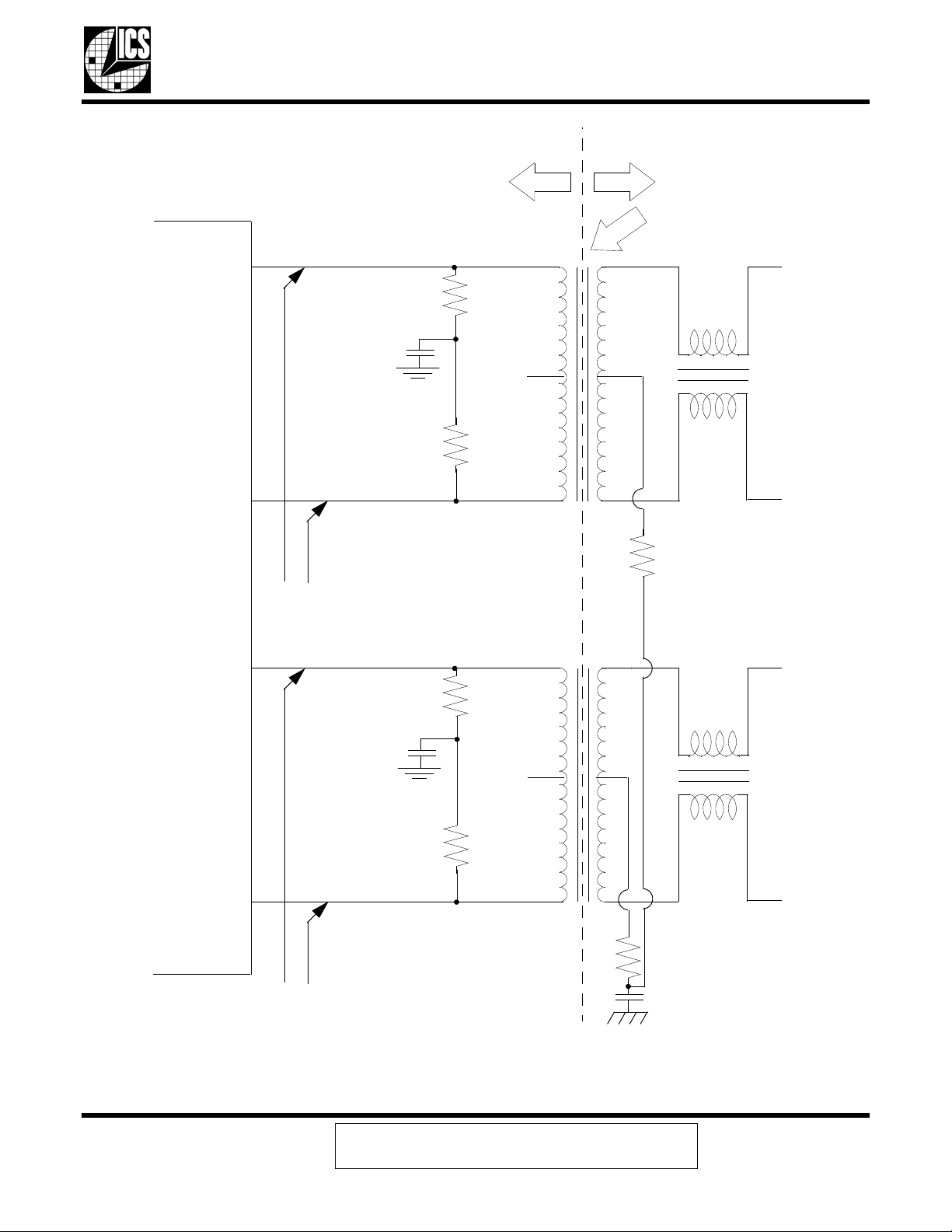
5.3 Twisted-Pair Interface
For the twisted-pair interface, the ICS1893CF uses 1:1 ratio transformers for both transmit and receive.
Better operation results from using a split ground plane through the transformer. In this case:
• The RJ-45 transformer windings must be on the chassis ground plane along with the Bob Smith
termination.
• The ICS1893CF system ground plane must include the ICS1893CF-side transformer windings along
with the 49.9Ω resistors and the 100 nF capacitor.
• The transformer provides the isolation with one set of windings on one ground plane and another set of
windings on the second ground plane.
Chapter 5 Interface OverviewsICS1893CF Data Sheet - Release
5.3.1 Twisted-Pair Transmitter
The twisted-pair transmitter driver uses an H-bridge configuration. IDT transformer requirements:
• Turns Ratio 1:1
• Chokes may be used on chip or cable side or both sides
• No power connections to the transformer. Transformer power is supplied by the ICS1893CF
• MIDCOM 7090-37 or equivalent symetrical magnetics are used
Figure 5-1 shows the design for the ICS1893CF twisted-pair interface.
• Two 49.9Ω 1% resistors are in series with a 100 nF capacitor to ground between them. These
components form a network that connects across both pairs of twisted pairs A and B.
• Both twisted pairs A and B have an assigned plus and minus.
Note:
1. Keep all TX traces as short as possible.
2. When longer board twisted pair traces are used, 50Ω-characteristic board trace impedance is
desirable.
ICS1893CF, Rev. F, 03/01/07 Mar. 2007
Copyright © 2007, Integrated Device Technology, Inc.
All rights reserved.
18
Page 19
ICS1893CF Data Sheet Rev. F - Release
Figure 5-1. ICS1893CF Twisted Pair *
System Ground Plane Chassis Ground Plane
TP_AP 12
49.9Ω 1%
Chapter 5 Interface Overviews
Separate Ground Plane
1:1
ICS1893CF
TP_AN 13
Ideally, for these traces Zo = 50Ω.
TP_BP 16
100 nF
49.9Ω 1%
49.9Ω 1%
100 nF
Center
Tap
NC
Center
Tap
NC
To RJ-45
75Ω
To RJ-45
49.9Ω 1%
TP_BN 15
75Ω
Ideally, for these traces Zo = 50Ω.
0.1 µF
Chassis GND
* For backward compatibility, refer to the the “1893C Alternate Schematic” application note.
ICS1893CF, Rev. F, 03/01/07 Mar. 2007
Copyright © 2007, Integrated Device Technology, Inc.
All rights reserved.
19
Page 20
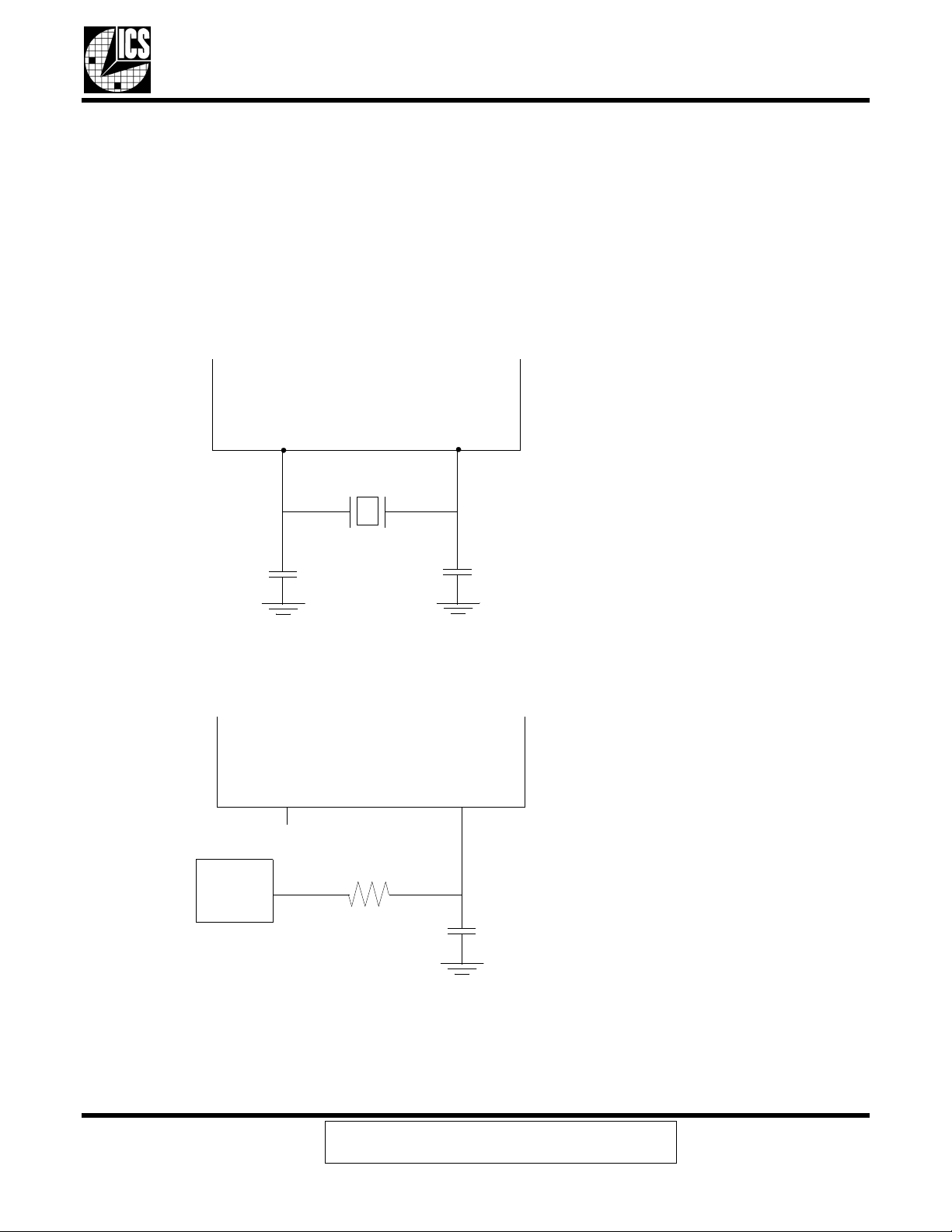
5.4 Clock Reference Interface
The REF_IN pin provides the ICS1893CF Clock Reference Interface. The ICS1893CF requires a single
clock reference with a frequency of 25 MHz ±50 parts per million. This accuracy is necessary to meet the
interface requirements of the ISO/IEEE 8802-3 standard, specifically clauses 22.2.2.1 and 24.2.3.4. The
ICS1893CF supports two clock source configurations: a CMOS oscillator or a CMOS driver. The input to
REF_IN is CMOS (10% to 90% VDD), not TTL. Alternately, a 25MHz crystal may be used. The Oscillator
specifications are shown in Table 5.2.
Figure 5-2. Crystal or Oscillator Operation
Crystal
ICS1893CF
Chapter 5 Interface OverviewsICS1893CF Data Sheet - Release
Oscillator
33 pF
REF_OUT
46
REF_OUT
46
NC
REF_IN
47
25.000MHz
33 pF
ICS1893CF
REF_IN
47
CMOS
33 Ohm
25.000
MHz
10 pF
ICS1893CF, Rev. F, 03/01/07 Mar. 2007
Copyright © 2007, Integrated Device Technology, Inc.
All rights reserved.
20
Page 21
ICS1893CF Data Sheet Rev. F - Release
Chapter 5 Interface Overviews
If a crystal is used as the clocking source, connect it to both the Ref_in (pin 47) and Ref_out (pin 46) pins
of the ICS1893CF. A pair of bypass capacitors on either side of the crystal are connected to ground. The
crystal is used in the parallel resonance or anti-resonance mode. The value of the load caps serve to adjust
the final frequency of the crystal oscillation. Typical applications would use 33pF load caps. The exact
value will be affected by the board routing capacitance on Ref_in and Ref_out pins. Smaller load capacitors
raise the frequency of oscillation. Once the exact value of load capacitance is established it will be the
same for all boards using the same specification crystal. The best way to measure the crystal frequency is
to measure the frequency of TXCLK (pin 37) using a frequency counter with a 1 second gate time. Using
the buffered output TXCLK prevents the crystal frequency from being affected by the measurement. The
crystal specification is shown in Table 5.1.
Table 5-1. 25MHz Crystal Specification
Specifications Symbol Minimum Typical Maximum Unit
Fundamental Frequency
F0 24.99875 25.00000 25.00125 MHz
(tolerance is sum of freq.,
temp., stability and aging.)
Freq. Tolerance
∆F/f ± 50 ppm
Input Capacitance Cin 3 pF
Table 5-2. 25MHz Oscillator Specification
Specifications Symbol Minimum Typical Maximum Unit
Output Frequency F0 24.99875 25.00000 25.00125 MHz
Freq. Stability (including aging)
Duty cycle CMOS level
∆F/f ± 50 ppm
Tw/T 35 65 %
one-half VDD
VIH 2.79 Volts
VIL 0.33 Volts
Period Jitter Tjitter 500 pS
Input Capacitance CIN 3 pF
ICS1893CF, Rev. F, 03/01/07 Mar. 2007
Copyright © 2007, Integrated Device Technology, Inc.
All rights reserved.
21
Page 22
5.5 Status Interface
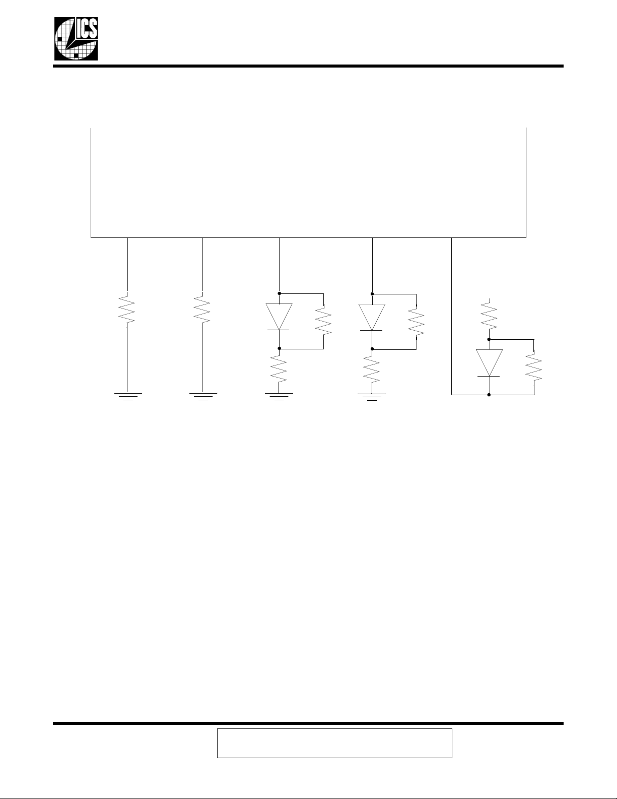
The ICS1893CF provides five multi-function configuration pins that report the results of continual link
monitoring by providing signals that are intended for driving LEDs. (For the pin numbers, see Table 8.6.)
Table 5-3. Pins for Monitoring the Data Link
Pin LED Driven by the Pin’s Output Signal
P0AC AC (Link Activity) LED
P1CL CL (Collisions) LED
P2LI LI (Link Integrity) LED
P3TD TD (Transmit Data) LED
P4RD RD (Receive Data) LED
Note:
1. During either a power-on reset or a hardware reset, each multi-function configuration pin is an input
that is sampled when the ICS1893CF exits the reset state. After sampling is complete, these pins are
output pins that can drive status LEDs.
2. A software reset does not affect the state of a multi-function configuration pin. During a software reset,
all multi-function configuration pins are outputs.
3. Each multi-function configuration pin must be pulled either up or down with a resistor to establish the
address of the ICS1893CF. LEDs may be placed in series with these resistors to provide a designated
status indicator as described in Table 5-3. Use 1KΩ resistors.
Chapter 5 Interface OverviewsICS1893CF Data Sheet - Release
Caution: All pins listed in Table 5-3 must not float.
4. As outputs, the asserted state of a multi-function configuration pin is the inverse of the sense sampled
during reset. This inversion provides a signal that can illuminate an LED during an asserted state. For
example, if a multi-function configuration pin is pulled down to ground through an LED and a
current-limiting resistor, then the sampled sense of the input is low. To illuminate this LED for the
asserted state, the output is driven high.
5. Adding 10KΩ resistors across the LEDs ensures the PHY address is fully defined during slow VDD
power-ramp conditions.
6. PHY address 00 tri-states the MII interface. (Do not select PHY address 00 unless you want the MII
tri-stated.)
ICS1893CF, Rev. F, 03/01/07 Mar. 2007
Copyright © 2007, Integrated Device Technology, Inc.
All rights reserved.
22
Page 23
ICS1893CF Data Sheet Rev. F - Release
Figure 5-3 shows typical biasing and LED connections for the ICS1893CF.
Figure 5-3. ICS1893CF LED - PHY Interface
ICS1893CF
P4RD P3TD P2LI P1CL P0AC
86 4 3 1
Chapter 5 Interface Overviews
10KΩ
REC
TRANS
10KΩ
LED
LINK ACTIVITY
10KΩ
LED
1KΩ
COL
10KΩ
1KΩ
LED
This circuit decodes to PHY address = 1.
Notes:
1. All LED pins must be set during reset.
2. Caution: PHY address 00 tri-states the MII interface. Don’t use PHY address 00.
3. For more reliable address capture during power-on reset, add a 10KΩ resistor across
the LED.
VDD
1KΩ
10KΩ
ICS1893CF, Rev. F, 03/01/07 Mar. 2007
Copyright © 2007, Integrated Device Technology, Inc.
All rights reserved.
23
Page 24

Chapter 6 Functional Blocks
This chapter discusses the following ICS1893CF functional blocks.
• Section 6.1, “Functional Block: Media Independent Interface”
• Section 6.2, “Functional Block: Auto-Negotiation”
• Section 6.3, “Functional Block: 100Base-X PCS and PMA Sublayers”
• Section 6.4, “Functional Block: 100Base-TX TP-PMD Operations”
• Section 6.5, “Functional Block: 10Base-T Operations”
• Section 6.6, “Functional Block: Management Interface”
Chapter 6 Functional BlocksICS1893CF Data Sheet - Release
ICS1893CF, Rev. F, 03/01/07 Mar. 2007
Copyright © 2007, Integrated Device Technology, Inc.
All rights reserved.
24
Page 25

ICS1893CF Data Sheet Rev. F - Release
6.1 Functional Block: Media Independent Interface
All ICS1893CF MII interface signals are fully compliant with the ISO/IEC 8802-3 standard. In addition, the
ICS1893CF MIIs can support two data transfer rates: 25 MHz (for 100Base-TX operations) and 2.5 MHz
(for 10Base-T operations).
The Media Independent Interface (MII) consists of two primary components:
1. An interface between a MAC (Media Access Control sublayer) and the PHY (that is, the ICS1893CF).
This MAC-PHY part of the MII consists of three subcomponents:
a. A synchronous Transmit interface that includes the following signals:
(1) A data nibble, TXD[3:0]
(2) A delimiter, TXEN
(3) A clock, TXCLK
b. A synchronous Receive interface that includes the followings signals:
(1) A data nibble, RXD[3:0]
(2) An error indicator, RXER
(3) A delimiter, RXDV
(4) A clock, RXCLK
c. A Media Status or Control interface that consists of a Carrier Sense signal (CRS) and a Collision
Detection signal (COL).
2. An interface between the PHY (the ICS1893CF) and an STA (Station Management entity). The
STA-PHY part of the MII is a two-wire, Serial Management Interface that consists of the following:
a. A clock (MDC)
b. A synchronous, bi-directional data signal (MDIO) that provides an STA with access to the
ICS1893CF Management Register set
Chapter 6 Functional Blocks
The ICS1893CF Management Register set (discussed in Chapter 7, “Management Register Set”) consists
of the following:
• Basic Management registers.
As defined in the ISO/IEC 8802-3 standard, these registers include the following:
– Control Register (register 0), which handles basic device configuration
– Status Register (register 1), which reports basic device capabilities and status
• Extended Management registers.
As defined in the ISO/IEC 8802-3 standard, the ICS1893CF supports Extended registers that provide
access to the Organizationally Unique Identifier and all auto-negotiation functionality.
• ICS (Vendor-Specific) Management registers.
The ICS1893CF provides vendor-specific registers for enhanced PHY operations. Among these is the
QuickPoll Detailed Status Register that provides a comprehensive and consolidated set of real-time PHY
information. Reading the QuickPoll register enables the MAC to obtain comprehensive status data with a
single register access.
ICS1893CF, Rev. F, 03/01/07 Mar. 2007
Copyright © 2007, Integrated Device Technology, Inc.
All rights reserved.
25
Page 26

6.2 Functional Block: Auto-Negotiation
The auto-negotiation logic of the ICS1893CF has the following main functions:
• To determine the capabilities of the remote link partner, (that is, the device at the other end of the link
segment’s medium or cable)
• To advertise the capabilities of the ICS1893CF to the remote link partner
• To establish a protocol with the remote link partner using the highest-performance operating mode that
they have in common
The design of the ICS1893CF Auto-Negotiation sublayer supports both legacy 10Base-T connections as
well as new connections that have multiple technology options for the link. For example, when the
ICS1893CF has the auto-negotiation process enabled and it is operating with a 10Base-T remote link
partner, the ICS1893CF monitors the link and automatically selects the 10Base-T operating mode – even
though the remote link partner does not support auto-negotiation. This process, called parallel detection, is
automatic and transparent to the remote link partner and allows the ICS1893CF to function seamlessly with
existing legacy network structures without any management intervention.
(For an overview of the auto-negotiation process, see Section 4.4, “Auto-Negotiation Operations”.)
6.2.1 Auto-Negotiation General Process
The Auto-Negotiation sublayer uses a physical signaling technique that is transparent at the packet level
and all higher protocol levels. This technique builds on the link pulse mechanism employed in 10Base-T
operations and is fully compliant with clause 28 of the ISO/IEC 8802-3 standard.
During the auto-negotiation process, both the ICS1893CF and its remote link partner use Fast Link Pulses
(FLPs) to simultaneously ‘advertise’ (that is, exchange) information on their respective technology
capabilities as follows:
1. For the auto-negotiation process to take place, both the ICS1893CF and its remote link partner must
first both support and be enabled for Auto-Negotiation.
2. The ICS1893CF obtains the data for its FLP bursts from the Auto-Negotiation Advertisement Register
(Register 4).
3. Both the ICS1893CF and the remote link partner substitute Fast Link Pulse (FLP) bursts in place of the
Normal Link Pulses (NLPs). In each FLP burst, the ICS1893CF transmits information on its technology
capability through its Link Control Word, which includes link configuration and status data.
4. Similarly, the ICS1893CF places the Auto-Negotiation data received from its remote link partner's FLP
bursts into the Auto-Negotiation Link Partner Ability Register (Register 5).
5. After the ICS1893CF and its remote link partner exchange technology capability information, the
ICS1893CF Auto-Negotiation sublayer contrasts the data in Registers 4 and 5 and automatically
selects for the operating mode the highest-priority technology that both Register 4 and 5 have in
common. (That is, both the ICS1893CF and its remote link partner use a predetermined priority list for
selecting the operating mode, thereby ensuring that both sides of the link make the same selection.) As
follows from Annex 28B of the ISO/IEC 8802-3 standard, the pre-determined technology priorities are
listed from 1 (highest priority) to 5 (lowest priority):
(1) 100Base-TX full duplex
(2) 100Base-T4. (The ICS1893CF does not support this technology.)
(3) 100Base-TX (half duplex)
(4) 10Base-T full duplex
(5) 10Base-T (half duplex)
Chapter 6 Functional BlocksICS1893CF Data Sheet - Release
ICS1893CF, Rev. F, 03/01/07 Mar. 2007
Copyright © 2007, Integrated Device Technology, Inc.
All rights reserved.
26
Page 27

ICS1893CF Data Sheet Rev. F - Release
6. To indicate that the auto-negotiation process is complete, the ICS1893CF sets bits 1.5 and 17.4 high to
logic one. After successful completion of the auto-negotiation process, the ICS1893CF
Auto-Negotiation sublayer performs the following steps:
a. It sets to logic one the Status Register’s Auto-Negotiation Complete bit (bit 1.5, which is also
available in the QuickPoll register as bit 17.4).
b. It enables the negotiated link technology (such as the 100Base Transmit modules and 100Base
Receive modules).
c. It disables the unused technologies to reduce the overall power consumption.
6.2.2 Auto-Negotiation: Parallel Detection
The ICS1893CF supports parallel detection. It is therefore compatible with networks that do not support the
auto-negotiation process. When enabled, the Auto-Negotiation sublayer can detect legacy 10Base-T link
partners as well as 100Base-TX link partners that do not have an auto-negotiation capability.
The Auto-Negotiation sublayer performs this parallel detection function when it does not get a response to
its FLP bursts. In these situations, the Auto-Negotiation sublayer performs the following steps:
1. It sets the LP_AutoNeg_Able bit (bit 6.0) to logic zero, thereby identifying the remote link partner as not
being capable of executing the auto-negotiation process.
2. It sets the bit in the Auto-Negotiation Link Partner Abilities Register that corresponds to the 'parallel
detected' technology [for example, half-duplex, 10Base-T (bit 5.5) or half-duplex, 100Base-TX (bit
5.7)].
3. It sets the Status Register’s Auto-Negotiation Complete bit (bit 1.5) to logic one, indicating completion
of the auto-negotiation process.
4. It enables the detected link technology and disables the unused technologies.
Chapter 6 Functional Blocks
A remote link partner that does not support the auto-negotiation process does not respond to the
transmitted FLP bursts. The ICS1893CF detects this situation and responds according to the data it
receives. The ICS1893CF can receive one of five potential responses to the FLP bursts it is transmitting:
FLP bursts, 10Base-T link pulses (that is, Normal Link Pulses), scrambled 100Base IDLEs, nothing, or a
combination of signal types.
A 10Base-T link partner transmits only Normal Link Pulses when idle. When the ICS1893CF receives
Normal Link Pulses, it concludes that the remote link partner is a device that can use only 10Base-T
technology. A 100Base-TX node without an Auto-Negotiation sublayer transmits 100M scrambled IDLE
symbols in response to the FLP bursts. Upon receipt of the scrambled IDLEs, the ICS1893CF concludes
that its remote link partner is a 100Base-TX node that does not support the auto-negotiation process. For
both 10Base-T and 100Base-TX nodes without an Auto-Negotiation sublayer, the ICS1893CF clears bit 6.0
to logic zero, indicating that the link partner cannot perform the auto-negotiation process.
If the remote link partner responds to the FLP bursts with FLP bursts, then the link partner is a 100Base-TX
node that can support the auto-negotiation process. In this case, the ICS1893CF sets to logic one the
Auto-Negotiation Expansion Register’s Link Partner Auto-Negotiation Ability bit (bit 6.0).
If the Auto-Negotiation sublayer does not receive any signal when monitoring the receive channel, then the
QuickPoll Detailed Status Register’s Signal Detect bit (bit 17.3) is set to logic one, indicating that no signal
is present.
Another possibility is that the ICS1893CF senses that it is receiving multiple technology indications. In this
situation, the ICS1893CF cannot determine which technology to enable. It informs the STA of this problem
by setting to logic one the Auto-Negotiation Expansion Register’s Parallel Detection Fault bit (bit 6.4).
ICS1893CF, Rev. F, 03/01/07 Mar. 2007
Copyright © 2007, Integrated Device Technology, Inc.
All rights reserved.
27
Page 28

6.2.3 Auto-Negotiation: Remote Fault Signaling
If the remote link partner detects a fault, the ICS1893CF reports the remotely detected fault to the STA by
setting to logic one the Remote Fault Detected bit(s), 1.4, 5.13, 17.1, and 19.13. In general, the reception
of a remote fault means that the remote link partner has a problem with the integrity of its receive channel.
Similarly, if the ICS1893CF detects a link fault, it transmits a remote fault-detected condition to its remote
link partner. In this situation, the ICS1893CF sets to logic one the Auto-Negotiation Link Partner Ability
Register’s Remote Fault Indication bit (bit 4.13).
For details, see Section 7.14.3, “Remote Fault (bit 19.13)” and Section 7.3.9, “Remote Fault (bit 1.4)”.
6.2.4 Auto-Negotiation: Reset and Restart
If enabled, execution of the ICS1893CF auto-negotiation process occurs at power-up and upon
management request. There are two primary ways to begin the Auto-Negotiation state machine:
• ICS1893CF reset
• Auto-Negotiation Restart
6.2.4.1 Auto-Negotiation Reset
During a reset, the ICS1893CF initializes its Auto-Negotiation sublayer modules to their default states.
(That is, the Auto-Negotiation Arbitration State Machine and the Auto-Negotiation Progress Monitor reset to
their idle states.) In addition, the Auto-Negotiation Progress Monitor status bits are all set to logic zero. This
action occurs for any type of reset (hardware reset, software reset, or power-on reset).
Chapter 6 Functional BlocksICS1893CF Data Sheet - Release
6.2.4.2 Auto-Negotiation Restart
As with a reset, during an Auto-Negotiation restart, the ICS1893CF initializes the Auto-Negotiation
Arbitration State Machine and the Auto-Negotiation Progress Monitor modules to their default states.
However, during an Auto-Negotiation Restart, the Auto-Negotiation Progress Monitor status bits maintain
their current state. Only three events can alter the state of the Auto-Negotiation Progress Monitor status
bits after a Restart: (1) an STA read operation, (2) a reset, or (3) the Auto-Negotiation Arbitration State
Machine progressing to a higher state or value.
The Auto-Negotiation Progress Monitor Status bits change only if they are progressing to a state with a
value greater than their current state (that is, a state with a higher logical value than that of their current
state). For a detailed explanation of these bits and their operation, see Section 6.2.5, “Auto-Negotiation:
Progress Monitor”.
After the Auto-Negotiation Arbitration State Machine reaches its final state (which is Auto-Negotiation
Complete), only an STA read of the QuickPoll Detailed Status Register or an ICS1893CF reset can alter
these status bits.
Any of the following situations initiates a restart of the ICS1893CF Auto-Negotiation sublayer:
• A link failure
• In software mode:
– Writing a logic one to the Control Register’s Restart Auto-Negotiation bit (bit 0.9), which is a self-
clearing bit.
– Toggling the Control Register’s Auto-Negotiation Enable bit (bit 0.12) from a logic one to a logic zero,
and back to a logic one.
ICS1893CF, Rev. F, 03/01/07 Mar. 2007
Copyright © 2007, Integrated Device Technology, Inc.
All rights reserved.
28
Page 29

ICS1893CF Data Sheet Rev. F - Release
6.2.5 Auto-Negotiation: Progress Monitor
Under typical circumstances, the Auto-Negotiation sublayer can establish a connection with the
ICS1893CF’s remote link partner. However, some situations can prevent the auto-negotiation process from
properly achieving this goal. For these situations, the ICS1893CF has an Auto-Negotiation Progress
Monitor to provide detailed status information to its Station Management (STA) entity. With this status
information, the STA can diagnose the failure mechanism and – in some situations – establish the link by
correcting the problem.
When enabled, the auto-negotiation process typically requires less than 500 ms to execute, independent of
the link partner's ability to perform the auto-negotiation process. Typically, an STA polls both the
Auto-Negotiation Complete bit (bit 1.5) and the Link Status bit (bit 1.2) to determine when a link is
successfully established, either through auto-negotiation or parallel detection. The STA can then poll the
Auto-Negotiation Link Partner Ability Register and determine the highest-performance operating mode in
common with the capabilities it is advertising.
6.3 Functional Block: 100Base-X PCS and PMA Sublayers
The ICS1893CF is fully compliant with clause 24 of the ISO/IEC specification, which defines the
100Base-X Physical Coding sublayer (PCS) and Physical Medium Attachment (PMA) sublayers.
6.3.1 PCS Sublayer
The ICS1893CF 100Base-X PCS sublayer provides two interfaces: one to a MAC and the other to the
ICS1893CF PMA sublayer. An ICS1893’s PCS sublayer performs the transmit, receive, and control
functions and consists of the following:
• PCS Transmit sublayer, which provides the following:
– Parallel-to-serial conversion
– 4B/5B encoding
– Collision detection
• PCS Receive sublayer, which provides the following:
– Serial-to-parallel conversion
– 4B/5B encoding
– Carrier detection
– Code group framing
• PCS control functions, which provide:
– Assertion of the CRS (carrier sense) signal
– Assertion of the COL (collision detection) signal
Chapter 6 Functional Blocks
6.3.2 PMA Sublayer
The ICS1893CF 100Base-X PMA Sublayer consists of two interfaces: one to the Physical Coding sublayer
and the other to the Physical Medium Dependent sublayer. Functionally, the PMA sublayer is responsible
for the following:
• Link Monitoring
• Carrier Detection
• NRZI encoding/decoding
• Transmit Clock Synthesis
• Receive Clock Recovery
ICS1893CF, Rev. F, 03/01/07 Mar. 2007
Copyright © 2007, Integrated Device Technology, Inc.
All rights reserved.
29
Page 30

6.3.3 PCS/PMA Transmit Modules
Both the PCS and PMA sublayers have Transmit modules.
6.3.3.1 PCS Transmit Module
The ICS1893CF PCS Transmit module accepts nibbles from the MAC Interface and converts the nibbles
into 5-bit ‘code groups’ (referred to here as ‘symbols’). In addition, the PCS Transmit module performs a
parallel-to-serial conversion on the symbols, and subsequently passes the resulting serial bit stream to the
PMA sublayer.
The first 16 nibbles of each MAC Frame represent the Frame Preamble. The PCS replaces the first two
nibbles of the Frame Preamble with the Start-of-Stream Delimiter (SSD), that is, the symbols /J/K/. After
receipt of the last Frame nibble, detected when TX_EN = FALSE, the PCS appends to the end of the Frame
an End-of-Stream Delimiter (ESD), that is, the symbols /T/R/. (The ICS1893CF PCS does not alter any
other data included within the Frame.)
The PCS Transmit module also performs collision detection. In compliance with the ISO/IEC specification,
when the transmission and reception of data occur simultaneously and the ICS1893CF is in:
• Half-duplex mode, the ICS1893CF asserts the collision detection signal (COL).
• Full-duplex mode, COL is always FALSE.
6.3.3.2 PMA Transmit Module
The ICS1893CF PMA Transmit module accepts a serial bit stream from its PCS and converts the data into
NRZI format. Subsequently, the PMA passes the NRZI bit stream to the Twisted-Pair Physical Medium
Dependent (TP-PMD) sublayer.
The ICS1893CF PMA Transmit module uses a digital PLL to synthesize a transmit clock from the Clock
Reference Interface.
Chapter 6 Functional BlocksICS1893CF Data Sheet - Release
6.3.4 PCS/PMA Receive Modules
Both the PCS and PMA sublayers have Receive modules.
6.3.4.1 PCS Receive Module
The ICS1893CF PCS Receive module accepts both a serial bit stream and a clock signal from the PMA
sublayer. The PCS Receive module converts the bit stream from a serial format to a parallel format and
then processes the data to detect the presence of a carrier.
When a link is in the idle state, the PCS Receive module receives IDLE symbols. (All bits are logic one.)
Upon receiving two non-contiguous zeros in the bit stream, the PCS Receive module examines the
ensuing bits and attempts to locate the Start-of-Stream Delimiter (SSD), that is, the /J/K/ symbols.
Upon verification of a valid SSD, the PCS Receive module substitutes the first two standard nibbles of a
Frame Preamble for the detected SSD. In addition, the PCS Receive module uses the SSD to begin
framing the ensuing data into 5-bit code symbols. The final PCS Receive module performs 4B/5B decoding
on the symbols and then synchronously passes the resulting nibbles to the MAC Interface.
The Receive state machine continues to accept PMA data, convert it from serial to parallel format, frame it,
decode it, and pass it to the MAC Interface. During this time, the Receive state machine alternates between
Receive and Data States. It continues this process until detecting one of the following:
• An End-of-Stream Delimiter (ESD, that is, the /T/R/ symbols)
• An error
• A premature end (IDLEs)
ICS1893CF, Rev. F, 03/01/07 Mar. 2007
Copyright © 2007, Integrated Device Technology, Inc.
All rights reserved.
30
Page 31

ICS1893CF Data Sheet Rev. F - Release
Upon receipt of an ESD, the Receive state machine returns to the IDLE state without passing the ESD to
the MAC Interface. Detection of an error forces the Receive state machine to assert the receive error signal
(RX_ER) and wait for the next symbol. If the ICS1893CF Receive state machine detects a premature end,
it forces the assertion of the RX_ER signal, sets the Premature End bit (bit 17.5) to logic one, and
transitions to the IDLE State.
6.3.4.2 PMA Receive Modules
The ICS1893CF has a PMA Receive module that provides the following functions:
• NRZI Decoding
The Receive module performs the NRZI decoding on the serial bit stream received from the Twisted-Pair
Physical Medium Dependent (TP-PMD) sublayer. It converts the bit stream to a unipolar, positive, binary
format that the PMA subsequently passes to the PCS.
• Receive Clock Recovery
The Receive Clock Recovery function consists of a phase-locked loop (PLL) that operates on the serial
data stream received from the PMD sublayer. This PLL automatically synchronizes itself to the clock
encoded in the serial data stream and then provides both a recovered clock and data stream to the PCS.
• Link Monitoring
– The ICS1893CF’s PMA Link Monitoring function observes the Receive Clock PLL. If the Receive
Clock PLL cannot acquire ‘lock’ on the serial data stream, it asserts an error signal. The status of this
error signal can be read in the QuickPoll Detailed Status Register’s PLL Lock Error bit (bit 17.9). This
bit is a latching high (LH) bit. (For more information on latching high and latching low bits, see Section
7.1.4.1, “Latching High Bits” and Section 7.1.4.2, “Latching Low Bits”.)
– In addition, the ICS1893CF’s PMA Link Monitor function continually audits the state of the connection
with the remote link partner. It asserts a receive channel error if a receive signal is not detected or if
a PLL Lock Error occurs. These errors, in turn, generate a link fault and force the link monitor
function to clear both the Status Register’s Link Status bit (bit 1.2) and the QuickPoll Detailed Status
Register’s Link Status bit (bit 17.0).
Chapter 6 Functional Blocks
6.3.5 PCS Control Signal Generation
For the PCS sublayer, there are two control signals: a Carrier Sense signal (CRS) and a Collision Detect
signal (COL).
The CRS control signals is generated as follows:
1. When a logic zero is detected in an idle bit stream, the Receive Functions examines the ensuing bits.
2. When the Receive Functions find the first two non-contiguous zero bits, the Receive state machine
moves into the Carrier Detect state.
3. As a result, the Boolean Receiving variable is set to TRUE.
4. Consequently, the Carrier Sense state machine moves into the Carrier Sense ‘on’ state, which asserts
the CRS signal.
5. If the PCS Functions:
a. Cannot confirm either the /I/J/ (IDLE, J) symbols or the /J/K/ symbols, the receive error signal
(RX_ER) is asserted, and the Receive state machine returns to the IDLE state. In IDLE, the
Boolean Receiving variable is set to FALSE, thereby causing the Carrier Sense state machine to
set the CRS signal to FALSE.
b. Can confirm the /I/J/K/ symbols, then the Receive state machine transitions to the ‘Receive’ state.
The COL control signal is generated by the transmit modules. For details, see Section 6.3.3.1, “PCS
Transmit Module”.
ICS1893CF, Rev. F, 03/01/07 Mar. 2007
Copyright © 2007, Integrated Device Technology, Inc.
All rights reserved.
31
Page 32

6.3.6 4B/5B Encoding/Decoding
The 4B/5B encoding methodology maps each 4-bit nibble to a 5-bit symbol (also called a “code group”).
There are 32 five-bit symbols, which include the following:
• Of the 32 five-bit symbols, 16 five-bit symbols are required to represent the 4-bit nibbles.
• The remaining 16 five-bit symbols are available for control functions. The IEEE Standard defines 6
symbols for control, and the remaining 10 symbols of this grouping are invalid. The 6 control symbols
include the following:
– /H/, which represents a Halt, also used to signify a Transmit Error
– /I/, which represents an IDLE
– /J/, which represents the first symbol of the Start-of-Stream Delimiter (SSD)
– /K/, which represents the second symbol of the Start-of-Stream Delimiter (SSD)
– /T/, which represents the first symbol of the End-of-Stream Delimiter (ESD)
– /R/, which represents the second symbol of the End-of-Stream Delimiter (ESD)
If the ICS1893CF PCS receives:
– One of the 10 undefined symbols, it sets its QuickPoll Detailed Status Register’s Invalid Symbol bit
(bit 17.7) to logic one.
– A Halt symbol, it sets the Halt Symbol Detected bit in its QuickPoll Detailed Status Register (bit 17.6)
to logic one.
Note: An STA can force the ICS1893CF to transmit symbols that are typically classified as invalid, by
both (1) setting the Extended Control Register’s Transmit Invalid Codes bit (bit 16.2) to logic one
and (2) asserting the associated TXER signal. For more information, see Section 7.11.7, “Invalid
Error Code Test (bit 16.2)”.
Chapter 6 Functional BlocksICS1893CF Data Sheet - Release
6.4 Functional Block: 100Base-TX TP-PMD Operations
The ICS1893CF supports both 10Base-T and 100Base-TX operations. For 100Base-TX operations, the
TP-PMD module performs stream-cipher scrambling/descrambling and MLT-3 encoding/decoding (3-level,
multi-level transition) in compliance with the ANSI Standard X3.263: 199X FDDI TP-PMD as defined in the
specification for 100Base-TX Twisted-Pair Physical Media Dependent (TP-PMD) Sublayer. The
ICS1893CF’s TP-PMD also performs DC restoration (that is, baseline wander correction) and adaptive
equalization on the received signals.
Note:
1. For an overview of 100Base-TX operations, see Section 4.5, “100Base-TX Operations”.
2. For more information on the Twisted-Pair Interface, see Section 5.3, “Twisted-Pair Interface”.
6.4.1 100Base-TX Operation: Stream Cipher Scrambler/Descrambler
When the ICS1893CF is operating in 100Base-TX mode, it employs a stream cipher
scrambler/descrambler that complies with the ANSI Standard X3.263: 199X FDDI TP-PMD. The purpose of
the stream cipher scrambler is to spread the transmission spectrum to minimize electromagnetic
compatibility problems. The stream cipher descrambler restores the received serial bit stream to its
unscrambled form.
The ICS1893CF “seeds” (that is, initializes) the Transmit Stream Cipher Shift register by using the
ICS1893CF PHY address from Table 7-16, which minimizes crosstalk and noise in repeater applications.
The MAC Interface bypasses the stream cipher scrambler/descrambler when in the 100M Symbol Interface
mode.
ICS1893CF, Rev. F, 03/01/07 Mar. 2007
Copyright © 2007, Integrated Device Technology, Inc.
All rights reserved.
32
Page 33

ICS1893CF Data Sheet Rev. F - Release
6.4.2 100Base-TX Operation: MLT-3 Encoder/Decoder
When operating in the 100Base-TX mode, the ICS1893CF TP-PMD sublayer employs an MLT-3 encoder
and decoder. During data transmission, the TP-PMD encoder converts the NRZI bit stream received from
the PMA sublayer to a 3-level Multi-Level Transition code. The three levels are -1, 0, and +1. The results of
MLT-3 encoding provide a reduction in the transmitted energy over the critical frequency range from 20
MHz to 100 MHz. The TP-PMD MLT-3 decoder converts the received three-level signal back to an NRZI bit
stream.
6.4.3 100Base-TX Operation: DC Restoration
The ICS1893CF’s 100Base-TX operations uses a stream-cipher scrambler to minimize peak amplitudes in
the frequency spectrum. However, the nature of the stream cipher and MLT-3 encoding is such that long
sequences of consecutive zeros or ones can exist. These unbalanced data patterns produce an
undesirable DC component in the data stream known as ‘baseline wander’.
Baseline wander adversely affects the noise immunity of the receiver, because the ‘baseline’ signal moves
or ‘wanders’ from its nominal DC value. The ICS1893CF uses a unique technique to restore the DC
component ‘lost’ by the medium. As a result, the design is very robust, immune to noise and independent
of the data stream.
6.4.4 100Base-TX Operation: Adaptive Equalizer
The ICS1893CF has a TP-PMD sublayer that uses adaptive equalization circuitry to compensate for signal
amplitude and phase distortion incurred from the transmission medium. At a data rate of 100 Mbps, the
transmission medium (that is, the cable) introduces significant signal distortion because of high-frequency
attenuation and phase shift. The high-frequency loss occurs primarily because of the cable skin effect that
causes the conductor resistance to rise as the square of the frequency rises.
Chapter 6 Functional Blocks
The ICS1893CF has an adaptive equalizer that accurately compensates for these losses in shielded
twisted-pair (STP) and unshielded twisted-pair (UTP) cables. The DSP-based adaptive equalizer uses a
technique that compensates for a wide range of cable lengths. The optimizing parameter for the
equalization process is the overall bit error rate of the ICS1893CF. This technique closes the loop on the
entire data reception process and provides a very high overall reliability.
6.4.5 100Base-TX Operation: Twisted-Pair Transmitter
The ICS1893CF uses the same Twisted-Pair Transmit pins (TP_TXP and TP_TXN) for both 10Base-T and
100Base-TX operations. Each twisted-pair transmitter module is a current-driven, differential driver that can
supply either of the following:
• A two-level 10Base-T (that is, Manchester-encoded) signal
• A three-level 100Base-TX (that is, MLT-3 encoded) signal
The ICS1893CF interfaces with the medium through an isolation transformer (sometimes referred to as a
magnetic module). The ICS1893CF’s transmitter uses wave-shaping techniques to control the output
signal rise and fall times (thereby eliminating the need for external filters) and interfaces directly to the
isolation transformer.
Note:
1. In reference to the ICS1893CF, the term ‘Twisted-Pair Transmitter’ refers to the set of Twisted-Pair
Transmit output pins (TP_TXP and TP_TXN).
2. For information on the 10Base-T Twisted-Pair Transmitter, see Section 6.5.11, “10Base-T Operation:
Twisted-Pair Transmitter”.
ICS1893CF, Rev. F, 03/01/07 Mar. 2007
Copyright © 2007, Integrated Device Technology, Inc.
All rights reserved.
33
Page 34

6.4.6 100Base-TX Operation: Twisted-Pair Receiver
The ICS1893CF uses the same Twisted-Pair Receive pins (TP_RXP and TP_RXN) for both 10Base-T and
100Base-TX operations. The internal twisted-pair receiver modules interface with the medium through an
isolation transformer. The 100Base-TX receiver module accepts and processes a differential three-level
100Base-TX (that is, MLT-3 encoded) signal from the isolation transformer. (In contrast, the 10Base-T
receiver module accepts and processes a differential two-level, Manchester- encoded, 10Base-T signal
from the isolation transformer).
Note:
1. In reference to the ICS1893CF, the term ‘Twisted-Pair Receiver’ refers to the set of Twisted-Pair
Receive output pins (TP_RXP and TP_RXN).
2. For information on the 10Base-T Twisted-Pair Receiver, see Section 6.5.12, “10Base-T Operation:
Twisted-Pair Receiver”.
6.4.7 100Base-TX Operation: Isolation Transformer
The ICS1893CF interfaces with a medium through isolation transformers. The PHY requires two isolation
transformers: one for its Twisted-Pair Transmitter and the other for its Twisted-Pair Receiver. These
isolation transformers provide both physical isolation as well as the means for coupling a signal between
the ICS1893CF and the medium for both 10Base-T and 100Base-TX operations.
Note: For information on isolation transformers (also referred to as magnetic modules), see Section 5.3,
“Twisted-Pair Interface”.
Chapter 6 Functional BlocksICS1893CF Data Sheet - Release
6.5 Functional Block: 10Base-T Operations
When configured for 10Base-T mode, the ICS1893CF MAC Interface is configured to provide 10M MII
(Media Independent Interface). The Twisted-Pair Interface is automatically configured to provide a
two-level, Manchester-encoded signal at the voltage levels specified in the ISO/IEC standard. (For more
information on the Twisted-Pair Interface, see Section 5.3, “Twisted-Pair Interface”.)
The 10Base-T and 100Base-TX operations differ as follows. 10Base-T operations are fundamentally
simpler than 100Base-TX operations. The data rate is slower, requiring less encoding than 100Base-TX
operations. In addition, the bandwidth requirements (and therefore the line attenuation issues) are not as
severe as with 100-MHz operations. Consequently, when an ICS1893CF is set for 10Base-T operations, it
requires fewer internal circuits in contrast to 100Base-TX operations. (For an overview of 10Base-T
operations, see Section 4.6, “10Base-T Operations”.).
6.5.1 10Base-T Operation: Manchester Encoder/Decoder
During data transmission the ICS1893CF acquires data from its MAC Interface in 4-bit nibbles. The
ICS1893CF converts this data into a Manchester-encoded signal for presentation to its MDI, as required by
the ISO/IEC specification.
In a Manchester-encoded signal, all logic:
• Ones are:
– Positive during the first half of the bit period
– Negative during the second half of the bit period
• Zeros are:
– Negative during the first half of the bit period
– Positive during the second half of the bit period
ICS1893CF, Rev. F, 03/01/07 Mar. 2007
Copyright © 2007, Integrated Device Technology, Inc.
All rights reserved.
34
Page 35

ICS1893CF Data Sheet Rev. F - Release
During 10Base-T data reception, a Manchester Decoder translates the serial bit stream obtained from the
Twisted-Pair Receiver (MDI) into an NRZ bit stream. The Manchester Decoder then passes the data to the
MAC Interface in parallel format.
Manchester-encoded signals have the following advantages:
• Every bit period has an encoded clock.
• The split-phase nature of the signal always provides a zero DC level regardless of the data (that is, there
is no baseline wander phenomenon).
The primary disadvantage in using Manchester-encoded signals is that it doubles the data rate, making it
operationally prohibitive for 100-MHz operations.
6.5.2 10Base-T Operation: Clock Synthesis
The ICS1893CF synthesizes the clocks required for synchronizing data transmission. In 10Base-T mode,
the MAC Interface provides a 10M MII (Media Independent Interface):
• 10M MII interface, the ICS1893CF synthesizes a 2.5-MHz clock for nibble-wide transactions
6.5.3 10Base-T Operation: Clock Recovery
The ICS1893CF recovers its receive clock from the Manchester-encoded data stream obtained from its
Twisted-Pair Receiver using a phase-locked loop (PLL). The ICS1893CF then uses this recovered clock for
synchronizing data transmission between itself and the MAC. Receive-clock PLL acquisitions begin with
reception of the MAC Frame Preamble and continue as long as the ICS1893CF is receiving data.
Chapter 6 Functional Blocks
6.5.4 10Base-T Operation: Idle
An ICS1893CF transmits Normal Link Pulses on its MDI in the absence of data. During this time the link is
Idle, and the ICS1893CF periodically transmits link pulses at a rate of one link pulse every 16 ms in
compliance with the ISO/IEC 8802-3 standard. In 10Base-T mode, the ICS1893CF continues transmitting link
pulses even while receiving data. This situation does not generate a Collision Detect signal (COL) because
link pulses indicate an idle state for a link.
6.5.5 10Base-T Operation: Link Monitor
When an ICS1893CF is in 10Base-T mode, its Link Monitor Function observes the data received by the
10Base-T Twisted-Pair Receiver to determine the link status. The results of this continual monitoring are
stored in the Link Status bit. The Station Management entity (STA) can access the Link Status bit in either
the Status Register (bit 1.2) or the QuickPoll Detailed Status Register (bit 17.0).
When the Link Status bit is:
• Zero, either a valid link is not established or the link is momentarily dropped since either the last read of
the Link Status bit or the last reset of the ICS1893CF.
• One, a valid link is established.
The ICS1893CF Link Status bit is a latching low (LL) bit. (For more information on latching high and latching
low bits, see Section 7.1.4.1, “Latching High Bits” and Section 7.1.4.2, “Latching Low Bits”.)
The criteria used by the Link Monitor Function to declare a link either valid or invalid depends upon these
factors: the present state of the link, whether its Smart Squelch function is enabled, and the incoming data.
ICS1893CF, Rev. F, 03/01/07 Mar. 2007
Copyright © 2007, Integrated Device Technology, Inc.
All rights reserved.
35
Page 36

Chapter 6 Functional BlocksICS1893CF Data Sheet - Release
When the 10Base-T link is:
• Invalid, and the Smart Squelch function is:
– Disabled (bit 18.0 is logic one), the Link Monitor Function must detect at least one of the following
events before transitioning its link from the invalid state to the valid state:
• More than seven, ISO/IEC-defined, Normal Link Pulses (NLPs)
• Any valid data
– Enabled (bit 18.0 is logic zero), the Link Monitor Function must detect at least one of the following
events before transitioning its link from the invalid state to the valid state:
• More than seven, ISO/IEC-defined, Normal Link Pulses (NLPs)
• Any valid data followed by a valid IDL
• Valid, and the Smart Squelch function is:
– Disabled (bit 18.0 is logic one), the Link Monitor Function continues to report its link as valid as long
as it continues to detect any of the following:
• ISO/IEC-defined, Normal Link Pulses (NLPs)
• Any valid data
– Enabled (bit 18.0 is logic zero), the Link Monitor Function continues to report its link as valid as long
as it continues to detect any of the following:
• ISO/IEC-defined, Normal Link Pulses (NLPs)
• Any valid data followed by a valid IDL
• Valid, the Link Monitor Function declares the link as invalid if it receives neither data nor NLPs (that is,
the link shows either no activity or inconsistent activity) for more than 81 to 83 ms. In this case the Link
Monitor Function sets the Link Status bit to logic zero.
Note:
1. An ICS1893CF receives ‘valid data’ when its Twisted-Pair Receiver phase-locked loop can acquire lock
and extract the receive clock from the incoming data stream for a minimum of three consecutive bit
times.
2. When a link is invalid and the Link Monitor Function detects the presence of data, the ICS1893CF does
not transition the link to the valid state until after the reception of the present packet is complete.
3. Enabling or disabling the Smart Squelch Function affects the Link Monitor function.
4. A transition from the invalid state to the valid state does not automatically update the latching-low Link
Status bit.
6.5.6 10Base-T Operation: Smart Squelch
The Smart Squelch Function imposes more stringent requirements on the Link Monitor Function regarding
the definition of a valid link, thereby providing a level of insurance that spurious noise is not mistaken for a
valid link during cable installation.
An STA can control the execution of the ICS1893CF Smart Squelch Function using bit 18.0 (the Smart
Squelch Inhibit bit in the 10Base-T Operations Register). When bit 18.0 is logic:
• Zero (the default), an ICS1893CF enables its Smart Squelch Function. In this case, the Link Monitor
must confirm the presence of both data and a valid IDL at the end of the packet before declaring a link
valid.
• One, an ICS1893CF disables or inhibits its Smart Squelch Function. In this case, the Link Monitor does
not have to confirm the presence of an IDL to declare a link valid (that is, the reception of any data is
sufficient).
In 10Base-T mode, an ICS1893CF appends an IDL to the end of each packet during data transmission.
The receiving PHY (the remote link partner) sees this IDL and removes it from the data stream.
ICS1893CF, Rev. F, 03/01/07 Mar. 2007
Copyright © 2007, Integrated Device Technology, Inc.
All rights reserved.
36
Page 37

ICS1893CF Data Sheet Rev. F - Release
6.5.7 10Base-T Operation: Carrier Detection
The ICS1893CF has a 10Base-T Carrier Detection Function that establishes the state of its Carrier Sense
signal (CRS), based upon the state of its Transmit and Receive state machines. These functions indicate
whether the ICS1893CF is (1) transmitting data, (2) receiving data, or (3) in a collision state (that is, the
ICS1893CF is both transmitting and receiving data on its twisted-pair medium, as defined in the ISO/IEC
8802-3 standard). When the ICS1893CF is configured for:
• Half-duplex operations, the ICS1893CF asserts its CRS signal when either transmitting or receiving
data.
• Full-duplex operations, the ICS1893CF asserts its CRS signal only when it is receiving data.
6.5.8 10Base-T Operation: Collision Detection
The ICS1893CF has a 10Base-T Collision Detection Function that establishes the state of its Collision
Detection signal (COL) based upon both (1) the state of its Receiver state machine and (2) the state of its
Transmit state machine. When the ICS1893CF is operating in:
• Half-duplex mode, the ICS1893CF asserts its COL signal to indicate it is receiving data while
transmission of data is also in progress.
• Full-duplex mode, the ICS1893CF always sets its COL signal to FALSE.
6.5.9 10Base-T Operation: Jabber
The ICS1893CF has an ISO/IEC compliant Jabber Detection Function that, when enabled, monitors the
data stream sent to its Twisted-Pair Transmitter to ensure that it does not exceed the 10Base-T Jabber
activation time limit (that is, the maximum transmission time). For more information, see Section 9.5.18,
“10Base-T: Jabber Timing”.
When the Jabber Detection Function detects that its transmission time exceeds the maximum Jabber
activation time limit and Jabber Detection is enabled, the ICS1893CF asserts its Collision Detect (COL)
signal. During this ISO/IEC specified ‘jabber de-activation time’, the ICS1893CF transmit data stream is
interrupted and prevented from reaching its Twisted-Pair Transmitter. During this time, when interrupting
the data stream and asserting its COL signal, the ICS1893CF transmits Normal Link Pulses and sets its
QuickPoll Detailed Status Register’s Jabber Detected bit (bit 17.2) to logic one. This bit is a latching high
(LH) bit. (For more information on latching high and latching low bits, see Section 7.1.4.1, “Latching High
Bits” and Section 7.1.4.2, “Latching Low Bits”.)
Chapter 6 Functional Blocks
The ICS1893CF provides an STA with the ability to disable the Jabber Detection Function using the Jabber
Inhibit bit (bit 18.5 in the 10Base-T Operations Register). Setting bit 18.5 to logic:
• Zero (the default) enables the Jabber Detection Function.
• One disables the Jabber Detection Function.
6.5.10 10Base-T Operation: SQE Test
The ICS1893CF has an ISO/IEC compliant Signal Quality Error (SQE) Test Function used exclusively for
10Base-T operations. When enabled, the ICS1893CF performs the SQE Test at the completion of each
transmitted packet (that is, whenever its TX_EN signal transitions from asserted to de-asserted). When the
ICS1893CF executes its SQE Test, it asserts the COL signal to its MAC Interface for a pre-determined time
duration (ISO/IEC specified). [For more information, see Section 9.5.17, “10Base-T: Heartbeat Timing
(SQE)”.]
ICS1893CF, Rev. F, 03/01/07 Mar. 2007
Copyright © 2007, Integrated Device Technology, Inc.
All rights reserved.
37
Page 38

An ICS1893CF SQE Test Function is:
• Enabled only when all the following conditions are true:
– The ICS1893CF is in node mode.
– The ICS1893CF is in half-duplex mode.
– The ICS1893CF has a valid link.
– The 10Base-T Operations Register’s SQE Test Inhibit bit (bit 18.2) is logic zero (the default).
– The ICS1893CF TX_EN signal has transitioned from asserted (high) to de-asserted (low).
• Disabled whenever any of the following are true:
– The ICS1893CF is in full-duplex mode.
– The ICS1893CF detects a link failure.
– The ICS1893CF SQE Test Inhibit bit (bit 18.2) in the 10Base-T Operations Register is logic one. [This
bit provides the Station Management entity (STA) with the ability to disable the SQE Test function.]
Note:
1. In 10Base-T mode, a bit time has a typical duration of 100 ns.
2. The SQE Test also has the name 10Base-T Heartbeat. For details on the SQE waveforms, see Section
9.5.17, “10Base-T: Heartbeat Timing (SQE)”.
6.5.11 10Base-T Operation: Twisted-Pair Transmitter
The 10Base-T Twisted-Pair Transmitter is functionally similar to the 100Base-TX Twisted-Pair Transmitter.
The primary differences are in the data rate and signaling, as specified in the ISO/IEC specifications. For
more information, see Section 6.4.5, “100Base-TX Operation: Twisted-Pair Transmitter”.
Chapter 6 Functional BlocksICS1893CF Data Sheet - Release
6.5.12 10Base-T Operation: Twisted-Pair Receiver
The 10Base-T Twisted-Pair Receiver is functionally similar the 100Base-TX Twisted-Pair Receiver. The
primary differences are in the data rate and signaling, as specified in the ISO/IEC specifications. For more
information, see Section 6.4.6, “100Base-TX Operation: Twisted-Pair Receiver”.
6.5.13 10Base-T Operation: Auto Polarity Correction
The ICS1893CF can sense and then automatically correct a signal polarity that is reversed on its
Twisted-Pair Receiver inputs. A signal polarity reversal occurs when the input signals on an ICS1893CF’s
TP_RXP and TP_RXN pins are crossed or swapped (a problem that can occur during network installation
or wiring).
The ICS1893CF accomplishes reversed signal polarity detection and correction by examining the signal
polarity of the Normal Link Pulses (NLPs). In 10Base-T mode, an ICS1893CF transmits and receives NLPs
when its link is in the Idle state. In 100Base-TX mode, an ICS1893CF transmits and receives NLPs during
Auto-Negotiation. An STA can control this feature using the 10Base-T Operations Register bit 18.3, the
Auto Polarity-Inhibit bit. When this bit is logic:
• Zero, the ICS1893CF automatically senses and corrects a reversed or inverted signal polarity on its
Twisted-Pair Receive pins (TP_RXP and TP_RXN).
• One, the ICS1893CF disables this feature.
ICS1893CF, Rev. F, 03/01/07 Mar. 2007
Copyright © 2007, Integrated Device Technology, Inc.
All rights reserved.
38
Page 39

ICS1893CF Data Sheet Rev. F - Release
When an ICS1893CF detects a reversed signal polarity on its Twisted-Pair Receiver pins and the Auto
Polarity-Inhibit bit is also logic zero (enabled), the ICS1893CF (1) automatically corrects the data stream
and (2) sets its Polarity Reversed bit (bit 18.14) to logic one, to indicate to the STA that this situation exists.
Bit 18.14 is a latching high (LH) bit. (For more information on latching high and latching low bits, see
Section 7.1.4.1, “Latching High Bits” and Section 7.1.4.2, “Latching Low Bits”.)
Note: The ICS1893CF will not complete the Auto-MDIX function for an inverted polarity cable. This
is a rare event with modern manufactured cables. Full Auto-Negotiation and Auto Polarity
Correction will complete when the Auto-MDIX function is disabled. Software control for the
Auto-MDIX function is available in MDIO Register 19 Bits 9:8.
6.5.14 10Base-T Operation: Isolation Transformer
The 10Base-T Isolation Transformer operates the same as the 100Base-TX Isolation Transformer. In fact,
in a typical ICS1893CF application they are the same unit. For more information, see Section 6.4.7,
“100Base-TX Operation: Isolation Transformer”.
6.6 Functional Block: Management Interface
As part of the MAC Interface, the ICS1893CF provides a two-wire serial management interface which
complies with the ISO/IEC 8802-3 standard MII Serial Management Interface. This interface is used to
exchange control, status, and configuration information between a Station Management entity (STA) and
the physical layer device (PHY). The PHY and STA exchange this data through a pre-defined set of
management registers. The ISO/IEC standard specifies the following components of this serial
management interface:
Chapter 6 Functional Blocks
• A set of registers (Section 6.6.1, “Management Register Set Summary”)
• The frame structure (Section 6.6.2, “Management Frame Structure”)
• The protocol
In compliance with the ISO/IEC specification, the ICS1893CF implementation of the serial management
interface provides a bi-directional data pin (MDIO) along with a clock (MDC) for synchronizing the
exchange of data. These pins remain active in all ICS1893CF MAC Interface modes (that is, the 10/100
MII, 100M Symbol, and 10M Serial interface modes).
6.6.1 Management Register Set Summary
The ICS1893CF implements a Management Register set that adheres to the ISO/IEC standard. This
register set (discussed in detail in Chapter 7, “Management Register Set”) includes the mandatory ‘Basic’
Control and Status registers and the ISO/IEC ‘Extended’ registers as well as some ICS-specific registers.
6.6.2 Management Frame Structure
The Serial Management Interface is a synchronous, bi-directional, two-wire, serial interface for the
exchange of configuration, control, and status data between a PHY, such as an ICS1893CF, and an STA.
All data transferred on an MDIO signal is synchronized by its MDC signal. The PHY and STA exchange
data through a pre-defined register set.
The ICS1893CF complies with the ISO/IEC defined Management Frame Structure and protocol. This
structure supports both read and write operations. Table 6-1 summarizes the Management Frame
Structure.
ICS1893CF, Rev. F, 03/01/07 Mar. 2007
Copyright © 2007, Integrated Device Technology, Inc.
All rights reserved.
39
Page 40

Note: The Management Frame Structure starts from and returns to an IDLE condition. However, the IDLE
periods are not part of the Management Frame Structure.
Table 6-1. Management Frame Structure Summary
Frame Field Data Comment
Acronym Frame Function
PRE Preamble (Bit 1.6) 11..11 32 ones
SFD Start of Frame 01 2 bits
OP Operation Code 10/01 (read/write) 2 bits
PHYAD PHY Address (Bits 16.10:6) AAAAA 5 bits
REGAD Register Address RRRRR 5 bits
TA Turnaround Z0/10 (read/write) 2 bits
DATA Data DDD..DD 16 bits
6.6.2.1 Management Frame Preamble
The ICS1893CF continually monitors its serial management interface for either valid data or a Management
Frame (MF) Preamble, based upon the setting of the MF Preamble Suppression bit, 1.6. When the MF
Preamble Suppression is disabled, an ICS1893CF waits for a MF Preamble which indicates the start of an
STA transaction. A Management Frame Preamble is a pattern of 32 contiguous logic one bits on the MDIO
pin, along with 32 corresponding clock cycles on the MDC pin.
Chapter 6 Functional BlocksICS1893CF Data Sheet - Release
The ICS1893CF supports the Management Frame (MF) Preamble Suppression capability on its
Management Interface, thereby providing a method to shorten the Management Frame and provide an STA
with faster access to the Management Registers.
The ability to process Management Frames that do not have a preamble is provided by the Management
Frame Preamble Suppression bit, (bit 1.6 in the ICS1893CF’s Status Register). This is an ISO/IEC defined
status bit that is intended to provide an indication of whether or not a PHY supports the MF Preamble
Suppression feature. In order to maintain backward compatibility with the ICS1890, which did not support
MF Preamble Suppression, the ICS1893CF MF Preamble Suppression bit is a Command Override Write
bit which defaults to a logic zero. An STA can enable MF Preamble Suppression by writing a logic one to bit
1.6 subsequent to a write of logic one to the Command Override bit, 16.15. For an explanation of the
Command Override Write bits, see Section 7.1.2, “Management Register Bit Access”.
6.6.2.2 Management Frame Start
A valid Management Frame includes a start-of-frame delimiter, SFD, immediately following the preamble.
The SFD bit pattern is 01b and is synchronous with two clock cycles on the MDC pin.
6.6.2.3 Management Frame Operation Code
A valid Management Frame includes an operation code (OP) immediately following the start-of-frame
delimiter. There are two valid operation codes: one for reading from a management register, 10b, and one
for writing to a management register, 01b. The ICS1893CF does not respond to the codes 00b and 11b,
which the ISO/IEC specification defines as invalid.
6.6.2.4 Management Frame PHY Address
The two-wire, Serial Management Interface is specified to allow busing (that is, the sharing of the two wires
among multiple PHYs). The Management Frame includes a 5-bit PHY Address field, PHYAD, allowing for
32 unique addresses. An STA uniquely identifies each of the PHYs that share a single serial management
interface by using this 5-bit PHY Address field, PHYAD.
ICS1893CF, Rev. F, 03/01/07 Mar. 2007
Copyright © 2007, Integrated Device Technology, Inc.
All rights reserved.
40
Page 41

ICS1893CF Data Sheet Rev. F - Release
Upon receiving a valid STA transaction, during a power-on or hardware reset an ICS1893CF compares the
PHYAD field included within the management frame with the value of its PHYAD bits stored in register 16.
(For information on the PHYAD bits, see Table 7-16.) An ICS1893CF responds to all transactions that
match its stored address bits.
6.6.2.5 Management Frame Register Address
A Management Frame includes a 5-bit register address field, REGAD. This field identifies which of the 32
Management Registers are involved in a transaction between an STA and a PHY.
6.6.2.6 Management Frame Operational Code
A management frame includes a 2-bit operational code field, OP. If the operation code is a:
• Read, the REGAD field identifies the register used as the source of data returned to the STA by the
ICS1893CF.
• Write, the REGAD identifies the destination register that is to receive the data sent by the STA to the
ICS1893CF.
6.6.2.7 Management Frame Turnaround
A valid management frame includes a turn-around field (TA), which is a 2-bit time space between the
REGAD field and the Data field. This time allows an ICS1893CF and an STA to avoid contentions during
read transactions. During an operation that is a:
• Read, an ICS1893CF remains in the high-impedance state during the first bit time and subsequently
drives its MDIO pin to logic zero for the second bit time.
• Write, an ICS1893CF waits while the STA transmits a logic one, followed by a logic zero on its MDIO pin.
Chapter 6 Functional Blocks
6.6.2.8 Management Frame Data
A valid management frame includes a 16-bit Data field for exchanging the register contents between the
ICS1893CF and the STA. All Management Registers are 16 bits wide, matching the width of the Data field.
During a transaction that is a:
• Read, (OP is 10b) the ICS1893CF obtains the contents of the register identified in the REGAD field and
returns this Data to the STA synchronously with its MDC signal.
• Write, (OP is 01b) the ICS1893CF stores the value of the Data field in the register identified in the
REGAD field.
If the STA attempts to:
• Read from a non-existent ICS1893CF register, the ICS1893CF returns logic one for all bits in the Data
field, FFFFh.
• Write to a non-existent ICS1893CF register, the ICS1893CF isolates the Data field of the management
frame from every reaching the registers.
Note: The first Data bit transmitted and received is the most-significant bit of a Management Register, bit
X.15.
6.6.2.9 Serial Management Interface Idle State
The MDIO signal is in an idle state during the time between STA transactions. When the Serial
Management Interface is in the idle state, the ICS1893CF disables (that is, tri-states) its MDIO pin, which
enters a high-impedance state. The ISO/IEC 8802-3 standard requires that an MDIO signal be idle for at
least one bit time between management transactions. However, the ICS1893CF does not have this
limitation and can support a continual bit stream on its MDIO signals.
ICS1893CF, Rev. F, 03/01/07 Mar. 2007
Copyright © 2007, Integrated Device Technology, Inc.
All rights reserved.
41
Page 42

Chapter 7 Management Register Set
The tables in this chapter detail the functionality of the bits in the management register set. The tables
include the register locations, the bit positions, the bit definitions, the STA Read/Write Access Types, the
default bit values, and any special bit functions or capabilities (such as self-clearing). Following each table
is a description of each bit. This chapter includes the following sections:
• Section 7.1, “Introduction to Management Register Set”
• Section 7.2, “Register 0: Control Register”
• Section 7.3, “Register 1: Status Register”
• Section 7.4, “Register 2: PHY Identifier Register”
• Section 7.5, “Register 3: PHY Identifier Register”
• Section 7.6, “Register 4: Auto-Negotiation Register”
• Section 7.7, “Register 5: Auto-Negotiation Link Partner Ability Register”
• Section 7.8, “Register 6: Auto-Negotiation Expansion Register”
• Section 7.9, “Register 7: Auto-Negotiation Next Page Transmit Register”
• Section 7.10, “Register 8: Auto-Negotiation Next Page Link Partner Ability Register”
• Section 7.11, “Register 16: Extended Control Register”
• Section 7.12, “Register 17: Quick Poll Detailed Status Register”
• Section 7.13, “Register 18: 10Base-T Operations Register”
• Section 7.14, “Register 19: Extended Control Register 2”
Chapter 7 Management Register SetICS1893CF Data Sheet - Release
ICS1893CF, Rev. F, 03/01/07 Mar. 2007
Copyright © 2007, Integrated Device Technology, Inc.
All rights reserved.
42
Page 43

ICS1893CF Data Sheet Rev. F - Release
7.1 Introduction to Management Register Set
This section explains in general terms the Management Register set discussed in this chapter. (For a
summary of the Management Register set, see Section 6.6.1, “Management Register Set Summary”.)
7.1.1 Management Register Set Outline
This section outlines the ICS1893CF Management Register set. Table 7-1 lists the ISO/IEC-specified
Management Register Set that the ICS1893CF implements.
Table 7-1. ISO/IEC-Specified Management Register Set
Register Address Register Name Basic / Extended
0 Control Basic
1Status Basic
2,3 PHY Identifier Extended
4 Auto-Negotiation Advertisement Extended
5 Auto-Negotiation Link Partner Ability Extended
6 Auto-Negotiation Expansion Extended
7 Auto-Negotiation Next Page Transmit Extended
8 Auto-Negotiation Next Page Link Partner Ability Extended
Chapter 7 Management Register Set
9 through 15 Reserved by IEEE Extended
16 through 31 Vendor-Specific (IDT) Registers Extended
Table 7-2 lists the IDT-specific registers that the ICS1893CF implements. These registers enhance the
performance of the ICS1893CF and provide the Station Management entity (STA) with additional control
and status capabilities.
Table 7-2. IDT-Specific Registers
Register Address Register Name Basic / Extended
16 Extended Control Extended
17 QuickPoll Detailed Status Extended
18 10Base-T Operations Extended
19 Extended Control 2 Extended
20 through 31 Reserved by IDT Extended
ICS1893CF, Rev. F, 03/01/07 Mar. 2007
Copyright © 2007, Integrated Device Technology, Inc.
All rights reserved.
43
Page 44

7.1.2 Management Register Bit Access
The ICS1893CF Management Registers include one or more of the following types of bits:
Table 7-3. Description of Management Register Bit Types
Chapter 7 Management Register SetICS1893CF Data Sheet - Release
Management
Register Bit Types
Read-Only RO An STA can obtain the value of a RO register bit. However, it cannot
Command Override
Write
Bit
Symbol
alter the value of (that is, it cannot write to) an RO register bit. The
ICS1893CF isolates any STA attempt to write a value to an RO bit.
CW An STA can read a value from a CW register bit. However, write
operations are conditional, based on the value of the Command
Register Override bit (bit 16.15). When bit 16.15 is logic:
• Zero (the default), the ICS1893CF isolates STA attempts to write to
the CW bits (that is, CW bits cannot be altered when bit 16.15 is
logic zero).
• One, the ICS1893CF permits an STA to alter the value of the CW
bits in the subsequent register write. (Bit 16.15 is self-clearing and
automatically clears to zero on the subsequent write.)
Read/Write R/W An STA can unconditionally read from or write to a R/W register bit.
Read/Write Zero R/W0 An STA can unconditionally read from a R/W0 register bit, but only a
‘0’ value can be written to this bit.
7.1.3 Management Register Bit Default Values
The tables in this chapter specify for each register bit the default value, if one exists. The ICS1893CF sets
all Management Register bits to their default values after a reset. Table 7-4 lists the valid default values for
ICS1893CF Management Register bits.
Description
Table 7-4. Range of Possible Valid Default Values for ICS1893CF Register Bits
Default Condition Default Value
– Indicates there is no default value for the bit
0 Indicates the bit’s default value is logic zero
1 Indicates the bit’s default value is logic one
State of pin at reset For some bits, the default value depends on the state (that is, the logic value) of a
particular pin at reset (that is, the logic value of a pin is latched at reset). An
example of pins that have a default condition that depends on the state of the pin
at reset are the PHY / LED pins (P0AC, P1CL, P2LI, P3TD, and P4RD) discussed
in the following sections:
• Section 5.5, “Status Interface”
• Section 7.11, “Register 16: Extended Control Register”
• Section 8.2.2, “Multi-Function (Multiplexed) Pins: PHY Address and LED Pins”
Note: The ICS1893CF has a number of reserved bits throughout the Management Registers. Most of
these bits provide enhanced test modes. The Management Register tables provide the default
values for these bits. The STA must not change the value of these bits under any circumstance. If
the STA inadvertently changes the default values of these reserved register bits, normal operation
of the ICS1893CF can be affected.
ICS1893CF, Rev. F, 03/01/07 Mar. 2007
Copyright © 2007, Integrated Device Technology, Inc.
All rights reserved.
44
Page 45

ICS1893CF Data Sheet Rev. F - Release
7.1.4 Management Register Bit Special Functions
This section discusses the types of special functions for the Management Register bits.
7.1.4.1 Latching High Bits
The purpose of a latching high (LH) bit is to record an event. An LH bit records an event by monitoring an
active-high signal and then latching this active-high signal when it triggers (that is, when the event occurs).
A latching high bit, once set to logic one, remains set until either a reset occurs or it is read by an STA.
Immediately following an STA read of an LH bit, the ICS1893CF latches the current state of the signal into
the LH bit. When an STA reads an LH bit:
• Once, the LL bit provides the STA with a history of whether or not the event has ever occurred. That is,
this first read provides the STA with a history of the condition and latches the current state of the signal
into the LL bit for the next read.
• Twice in succession, the LH bit provides the STA with the current state of the monitored signal.
7.1.4.2 Latching Low Bits
As with latching high bits, the purpose of a latching low (LL) bit is also to record an event. An LL bit records
an event by monitoring an active-low signal and then latching this active-low signal when it triggers (that is,
when the event occurs).
A latching low bit, once cleared to logic zero, remains cleared until either a reset occurs or it is read by an
STA. Immediately following an STA read of an LL bit, the ICS1893CF latches the current state of the
active-low signal into the LL bit. When an STA reads an LL bit:
Chapter 7 Management Register Set
• Once, the LL bit provides the STA with a history of whether or not the event has ever occurred. That is,
this first read provides the STA with a history of the condition and latches the current state of the signal
into the LL bit for the next read.
• Twice in succession, the LL bit provides the STA with the current state of the monitored signal.
7.1.4.3 Latching Maximum Bits
For the ICS1893CF, the purpose of latching maximum (LMX) bits is to track the progress of internal state
machines. The LMX bits act in combination with other LMX bits to save the maximum collective value of a
defined group of LMX bits, from the most-significant bit to the least-significant bit.
For example, assume a group of LMX bits is defined as register bits 13 through 11. If these bits first have a
value of 3o (octal) and then the state machine they are monitoring advances to state:
• 2o, then the 2o value does not get latched.
• 4o (or any other value greater than 3o), then in this case, the value of 4o does get latched.
LMX bits retain their value until either a reset occurs or they are read by an STA. Immediately following an
STA read of a defined group of LMX bits, the ICS1893CF latches the current state of the monitored state
machine into the LMX bits. When an STA reads a group of LMX bits:
• Once, the LMX bits provide the STA with a history of the maximum value that the state machine has
achieved and latches the current state of the state machine into the LMX bits for the next read.
• Twice in succession, the LMX bits provide the STA with the current state of the monitored state machine.
7.1.4.4 Self-Clearing Bits
Self-clearing (SC) bits automatically clear themselves to logic zero after a pre-determined amount of time
without any further STA access. The SC bits have a default value of logic zero and are triggers to begin
execution of a function. When the STA writes a logic one to an SC bit, the ICS1893CF begins executing the
function assigned to that bit. After the ICS1893CF completes executing the function, it clears the bit to
indicate that the action is complete.
ICS1893CF, Rev. F, 03/01/07 Mar. 2007
Copyright © 2007, Integrated Device Technology, Inc.
All rights reserved.
45
Page 46

7.2 Register 0: Control Register
Table 7-5 lists the bits for the Control Register, a 16-bit register used to establish the basic operating modes
of the ICS1893CF.
• The Control Register is accessible through the MII Management Interface.
• Its operation is independent of the MAC Interface configuration.
• It is fully compliant with the ISO/IEC Control Register definition.
Note: For an explanation of acronyms used in Table 7-5, see Chapter 1, “Abbreviations and Acronyms”.
Table 7-5. Control Register (Register 0 [0x00]
Chapter 7 Management Register SetICS1893CF Data Sheet - Release
Bit Definition When Bit = 0 When Bit = 1 Ac-
cess
0.15 Reset No effect ICS1893CF enters Reset
mode
0.14 Loopback enable Disable Loopback mode Enable Loopback mode R/W – 0
0.13 Data rate select 10 Mbps operation 100 Mbps operation R/W – 1
0.12 Auto-Negotiation enable Disable Auto-Negotiation Enable Auto-Negotiation R/W – 1
0.11 Low-power mode Normal power mode Low-power mode R/W – 0 0/4†
0.10 Isolate No effect Isolate ICS1893CF from
MII
0.9 Auto-Negotiation restart No effect Restart Auto-Negotiation R/W SC 0
0.8 Duplex mode Half-duplex operation Full-duplex operation R/W – 0
0.7 Collision test No effect Enable collision test R/W – 0 0
0.6 IEEE reserved Always 0 N/A RO – 0‡
0.5 IEEE reserved Always 0 N/A RO – 0‡
0.4 IEEE reserved Always 0 N/A RO – 0‡
0.3 IEEE reserved Always 0 N/A RO – 0‡ 0
0.2 IEEE reserved Always 0 N/A RO – 0‡
0.1 IEEE reserved Always 0 N/A RO – 0‡
0.0 IEEE reserved Always 0 N/A RO – 0‡
R/W SC 0 3
R/W – 0/1†
SF De-
fault
Hex
† Whenever the PHY address of Table 7-16:
• Is equal to 00000 (binary), the Isolate bit 0.10 is logic one.
• Is not equal to 00000, the Isolate bit 0.10 is logic zero.
‡ As per the IEEE Std 802.3u, during any write operation to any bit in this register, the STA must write the default value
to all Reserved bits.
7.2.1 Reset (bit 0.15)
This bit controls the software reset function. Setting this bit to logic one initiates an ICS1893CF software
reset during which all Management Registers are set to their default values and all internal state machines
are set to their idle state. For a detailed description of the software reset process, see Section 4.1.2.3,
“Software Reset”.
During reset, the ICS1893CF leaves bit 0.15 set to logic one and isolates all STA management register
accesses. However, the reset process is not complete until bit 0.15 (a Self-Clearing bit), is set to logic zero,
which indicates the reset process is terminated.
ICS1893CF, Rev. F, 03/01/07 Mar. 2007
Copyright © 2007, Integrated Device Technology, Inc.
All rights reserved.
46
Page 47

ICS1893CF Data Sheet Rev. F - Release
7.2.2 Loopback Enable (bit 0.14)
This bit controls the Loopback mode for the ICS1893CF. Setting this bit to logic:
• Zero disables the Loopback mode.
• One enables the Loopback mode by disabling the Twisted-Pair Transmitter, the Twisted-Pair Receiver,
and the collision detection circuitry. (The STA can override the ICS1893CF from disabling the collision
detection circuitry in Loopback mode by writing logic one to bit 0.7.) When the ICS1893CF is in
Loopback mode, the data presented at the MAC transmit interface is internally looped back to the MAC
receive interface. The delay from the assertion of Transmit Data Enable (TXEN) to the assertion of
Receive Data valid (RXDV) is less than 512 bit times.
7.2.3 Data Rate Select (bit 0.13)
This bit provides a means of controlling the ICS1893CF data rate. Its operation depends on the state of
several other functions, including the HW/SW input pin and the Auto-Negotiation Enable bit (bit 0.12).
When the ICS1893CF is configured for:
• Hardware mode (that is, the HW/SW pin is logic zero), the ICS1893CF isolates this bit 0.13 and uses the
10/100SEL input pin to establish the data rate for the ICS1893CF. In this Hardware mode:
– Bit 0.13 is undefined.
– The ICS1893CF provides a Data Rate Status bit (in the QuickPoll Detailed Status Register, bit
17.15), which always shows the setting of an active link.
• Software mode (that is, the HW/SW pin is logic one), the function of bit 0.13 depends on the
Auto-Negotiation Enable bit 0.12. When the Auto-Negotiation sublayer is:
– Enabled, the ICS1893CF isolates bit 0.13 and relies on the results of the auto-negotiation process to
establish the data rate.
– Disabled, bit 0.13 determines the data rate. In this case, setting bit 0.13 to logic:
• Zero selects 10-Mbps ICS1893CF operations.
• One selects 100-Mbps ICS1893CF operations.
Chapter 7 Management Register Set
7.2.4 Auto-Negotiation Enable (bit 0.12)
This bit provides a means of controlling the ICS1893CF Auto-Negotiation sublayer. Its operation depends
on the HW/SW input pin.
When the ICS1893CF is configured for:
• Hardware mode, (that is, the HW/SW pin is logic zero), the ICS1893CF isolates bit 0.12 and uses the
ANSEL (Auto-Negotiation Select) input pin to determine whether to enable the Auto-Negotiation
sublayer.
Note: In Hardware mode, bit 0.12 is undefined.
• Software mode, (that is, the HW/SW pin is logic one), bit 0.12 determines whether to enable the
Auto-Negotiation sublayer. When bit 0.12 is logic:
– Zero:
• The ICS1893CF disables the Auto-Negotiation sublayer.
• The ICS1893CF bit 0.13 (the Data Rate bit) and bit 0.8 (the Duplex Mode bit) determine the data
rate and the duplex mode.
– One:
• The ICS1893CF enables the Auto-Negotiation sublayer.
• The ICS1893CF isolates bit 0.13 and bit 0.8.
ICS1893CF, Rev. F, 03/01/07 Mar. 2007
Copyright © 2007, Integrated Device Technology, Inc.
All rights reserved.
47
Page 48

7.2.5 Low Power Mode (bit 0.11)
This bit provides one way to control the ICS1893CF low-power mode function. When bit 0.11 is logic:
• Zero, there is no impact to ICS1893CF operations.
• One, the ICS1893CF enters the low-power mode. In this case, the ICS1893CF disables all internal
functions and drives all MAC output pins low except for those that support the MII Serial Management
Port. In addition, the ICS1893CF internally activates the TPTRI function to tri-state the signals on the
Twisted-Pair Transmit pins (TP_TXP and TP_TXN) and achieve additional power savings.
Note: There are two ways the ICS1893CF can enter low-power mode. When entering low-power mode:
• By setting bit 0.11 to logic one, the ICS1893CF maintains the value of all Management Register
bits except the latching high (LH) and latching low (LL) status bits, which are re-initialized to their
default values instead. (For more information on latching high and latching low bits, see Section
7.1.4.1, “Latching High Bits” and Section 7.1.4.2, “Latching Low Bits”.)
• During a reset, the ICS1893CF sets all management register bits to their default values.
7.2.6 Isolate (bit 0.10)
This bit controls the ICS1893CF Isolate function. When bit 0.10 is logic:
• Zero, there is no impact to ICS1893CF operations.
• One, the ICS1893CF electrically isolates its data paths from the MAC Interface. The ICS1893CF places
all MAC output signals (TXCLK, RXCLK, RXDV, RXER, RXD[3:0], COL, and CRS) in a high-impedance
state and it isolates all MAC input signals (TXD[3:0], TXEN, and TXER). In this mode, the Serial
Management Interface continues to operate normally (that is, bit 0.10 does not affect the Management
Interface).
The default value for bit 0.10 depends upon the PHY address of Table 7-16. If the PHY address:
• Is equal to 00000b, then the default value of bit 0.10 is logic one, and the ICS1893CF isolates itself from
the MAC Interface.
• Is not equal to 00000b, then the default value of bit 0.10 is logic zero, and the ICS1893CF does not
isolate its MAC Interface.
Chapter 7 Management Register SetICS1893CF Data Sheet - Release
7.2.7 Restart Auto-Negotiation (bit 0.9)
This bit allows an STA to restart the auto-negotiation process in Software mode (that is, the HW/SW pin is
logic one). When bit 0.12 is logic:
• Zero, the Auto-Negotiation sublayer is disabled, and the ICS1893CF isolates any attempt by the STA to
set bit 0.9 to logic one.
• One (as set by an STA), the ICS1893CF restarts the auto-negotiation process. Once the
auto-negotiation process begins, the ICS1893CF automatically sets this bit to logic zero, thereby
providing the self-clearing feature.
ICS1893CF, Rev. F, 03/01/07 Mar. 2007
Copyright © 2007, Integrated Device Technology, Inc.
All rights reserved.
48
Page 49

ICS1893CF Data Sheet Rev. F - Release
7.2.8 Duplex Mode (bit 0.8)
This bit provides a means of controlling the ICS1893CF Duplex Mode. Its operation depends on several
other functions, including the HW/SW input pin and the Auto-Negotiation Enable bit (bit 0.12). When the
ICS1893CF is configured for:
• Hardware mode (that is, the HW/SW pin is logic zero), the ICS1893CF isolates bit 0.8 and uses the
DPXSEL input pin to establish the Duplex mode for the ICS1893CF. In this Hardware mode:
– Bit 0.8 is undefined.
– The ICS1893CF provides a Duplex Mode Status bit (in the QuickPoll Detailed Status Register, bit
17.14), which always shows the setting of an active link.
• Software mode (that is, the HW/SW pin is logic one), the function of bit 0.8 depends on the
Auto-Negotiation Enable bit, 0.12. When the auto-negotiation process is:
– Enabled, the ICS1893CF isolates bit 0.8 and relies upon the results of the auto-negotiation process
to establish the duplex mode.
– Disabled, bit 0.8 determines the Duplex mode. Setting bit 0.8 to logic:
• Zero selects half-duplex operations.
• One selects full-duplex operations. (When the ICS1893CF is operating in Loopback mode, it
isolates bit 0.8, which has no effect on the operation of the ICS1893CF.)
7.2.9 Collision Test (bit 0.7)
This bit controls the ICS1893CF Collision Test function. When an STA sets bit 0.7 to logic:
Chapter 7 Management Register Set
• Zero, the ICS1893CF disables the collision detection circuitry for the Collision Test function. In this case,
the COL signal does not track the TXEN signal. (The default value for this bit is logic zero, that is,
disabled.)
• One, as per the ISO/IEE 8802-3 standard, clause 22.2.4.1.9, the ICS1893CF enables the collision
detection circuitry for the Collision Test function, even if the ICS1893CF is in Loopback mode (that is, bit
0.14 is set to 1). In this case, the Collision Test function tracks the Collision Detect signal (COL) in
response to the TXEN signal. The ICS1893CF asserts the Collision signal (COL) within 512 bit times of
receiving an asserted TXEN signal, and it de-asserts COL within 4 bit times of the de-assertion of the
TXEN signal.
7.2.10 IEEE Reserved Bits (bits 0.6:0)
The IEEE reserves these bits for future use. When an STA:
• Reads a reserved bit, the ICS1893CF returns a logic zero.
• Writes to a reserved bit, it must use the default value specified in this data sheet.
The ICS1893CF uses some reserved bits to invoke auxiliary functions. To ensure proper operation of the
ICS1893CF, an STA must maintain the default value of these bits. Therefore, ICS recommends that during
any STA write operation, an STA write the default value to all reserved bits, even those bits that are Read
Only.
ICS1893CF, Rev. F, 03/01/07 Mar. 2007
Copyright © 2007, Integrated Device Technology, Inc.
All rights reserved.
49
Page 50

7.3 Register 1: Status Register
Table 7-6 lists the Status Register bits. These 16 bits of data provide an interface between the ICS1893CF
and an STA. There are two types of status bits: some report the capabilities of the port, and some indicate
the state of signals used to monitor internal circuits.
The STA accesses the Status Register using the Serial Management Interface. During a reset, the
ICS1893CF initializes the Status Register bits to pre-defined, default values.
Note: For an explanation of acronyms used in Table 7-5, see Chapter 1, “Abbreviations and Acronyms”.
Table 7-6. Status Register (Register 1 [0x01])
Chapter 7 Management Register SetICS1893CF Data Sheet - Release
Bit Definition When Bit = 0 When Bit = 1 Ac-
cess
1.15 100Base-T4 Always 0. (Not supported.) N/A RO – 0 7
1.14 100Base-TX full duplex Mode not supported Mode supported CW – 1
1.13 100Base-TX half duplex Mode not supported Mode supported CW – 1
1.12 10Base-T full duplex Mode not supported Mode supported CW – 1
1.11 10Base-T half duplex Mode not supported Mode supported CW – 1 8
1.10 IEEE reserved Always 0 N/A CW – 0†
1.9 IEEE reserved Always 0 N/A CW – 0†
1.8 IEEE reserved Always 0 N/A CW – 0†
1.7 IEEE reserved Always 0 N/A CW – 0† 0
1.6 MF Preamble
suppression
1.5 Auto-Negotiation
complete
1.4 Remote fault No remote fault detected Remote fault detected RO LH 0
1.3 Auto-Negotiation ability N/A Always 1: PHY has
1.2 Link status Link is invalid/down Link is valid/established RO LL 0
1.1 Jabber detect No jabber condition Jabber condition
1.0 Extended capability N/A Always 1: PHY has
PHY requires MF
Preambles
Auto-Negotiation is in
process, if enabled
PHY does not require
MF Preambles
Auto-Negotiation is
completed
Auto-Negotiation ability
detected
extended capabilities
SF De-
fault
RO – 0
RO LH 0
RO – 1 9
RO LH 0
RO – 1
Hex
† As per the IEEE Std 802.3u, during any write operation to any bit in this register, the STA must write the default value
to all Reserved bits.
7.3.1 100Base-T4 (bit 1.15)
The STA reads this bit to learn if the ICS1893CF can support 100Base-T4 operations. Bit 1.15 of the
ICS1893CF is permanently set to logic zero, which informs an STA that the ICS1893CF cannot support
100Base-T4 operations.
ICS1893CF, Rev. F, 03/01/07 Mar. 2007
Copyright © 2007, Integrated Device Technology, Inc.
All rights reserved.
50
Page 51

ICS1893CF Data Sheet Rev. F - Release
7.3.2 100Base-TX Full Duplex (bit 1.14)
The STA reads this bit to learn if the ICS1893CF can support 100Base-TX, full-duplex operations. The
ISO/IEC specification requires that the ICS1893CF must set bit 1.14 to logic:
• Zero if it cannot support 100Base-TX, full-duplex operations.
• One if it can support 100Base-TX, full-duplex operations. (For the ICS1893CF, the default value of bit
1.14 is logic one, in that the ICS1893CF supports 100Base-TX, full-duplex operations.)
Bit 1.14 is a Command Override Write bit, which allows an STA to alter the default value of this bit. [See the
description of bit 16.15, the Command Override Write Enable bit, in Section 7.11, “Register 16: Extended
Control Register”.]
7.3.3 100Base-TX Half Duplex (bit 1.13)
The STA reads this bit to learn if the ICS1893CF can support 100Base-TX, half-duplex operations. The
ISO/IEC specification requires that the ICS1893CF must set bit 1.13 to logic:
• Zero if it cannot support 100Base-TX, half-duplex operations.
• One if it can support 100Base-TX, half-duplex operations. (For the ICS1893CF, the default value of bit
1.13 is logic one. Therefore, when an STA reads the Status Register, the STA is informed that the
ICS1893CF supports 100Base-TX, half-duplex operations.)
This bit 1.13 is a Command Override Write bit, which allows an STA to alter the default value of this bit.
[See the description of bit 16.15, the Command Override Write Enable bit, in Section 7.11, “Register 16:
Extended Control Register”.]
Chapter 7 Management Register Set
7.3.4 10Base-T Full Duplex (bit 1.12)
The STA reads this bit to learn if the ICS1893CF can support 10Base-T, full-duplex operations. The
ISO/IEC specification requires that the ICS1893CF must set bit 1.12 to logic:
• Zero if it cannot support 10Base-T, full-duplex operations.
• One if it can support 10Base-T, full-duplex operations. (For the ICS1893CF, the default value of bit 1.12
is logic one. Therefore, when an STA reads the Status Register, the STA is informed that the ICS1893CF
supports 10Base-T, full-duplex operations.)
This bit 1.12 is a Command Override Write bit, which allows an STA to alter the default value of this bit.
[See the description of bit 16.15, the Command Override Write Enable bit, in Section 7.11, “Register 16:
Extended Control Register”.]
7.3.5 10Base-T Half Duplex (bit 1.11)
The STA reads this bit to learn if the ICS1893CF can support 10Base-T, half-duplex operations. The
ISO/IEC specification requires that the ICS1893CF must set bit 1.11 to logic:
• Zero if it cannot support 10Base-T, half-duplex operations.
• One if it can support 10Base-T, half-duplex operations. (For the ICS1893CF, the default value of bit 1.11
is logic one. Therefore, when an STA reads the Status Register, the STA is informed that the ICS1893CF
supports 10Base-T, half-duplex operations.)
Bit 1.11 of the ICS1893CF Status Register is a Command Override Write bit., which allows an STA to alter
the default value of this bit. [See the description of bit 16.15, the Command Override Write Enable bit, in
Section 7.11, “Register 16: Extended Control Register”.]
ICS1893CF, Rev. F, 03/01/07 Mar. 2007
Copyright © 2007, Integrated Device Technology, Inc.
All rights reserved.
51
Page 52

7.3.6 IEEE Reserved Bits (bits 1.10:7)
The IEEE reserves these bits for future use. When an STA:
• Reads a reserved bit, the ICS1893CF returns a logic zero.
• Writes a reserved bit, the STA must use the default value specified in this data sheet.
Both the ISO/IEC standard and the ICS1893CF reserve the use of some Management Register bits. ICS
uses some reserved bits to invoke ICS1893CF test functions. To ensure proper operation of the
ICS1893CF, an STA must maintain the default value of these bits. Therefore, ICS recommends that an STA
write the default value to all reserved bits during all Management Register write operations.
Reserved bits 1.10:7 are Command Override Write (CW) bits. When bit 16.15, the Command Register
Override bit, is logic:
• Zero, the ICS1893CF prevents all STA writes to CW bits.
• One, an STA can modify the value of these bits.
7.3.7 MF Preamble Suppression (bit 1.6)
Status Register bit 1.6 is the Management Frame (MF) Preamble Suppression bit. The ICS1893CF sets bit
1.6 to inform the STA of its ability to receive frames that do not have a preamble. When this bit is logic:
• Zero, the ICS1893CF is indicating it cannot accept frames with a suppressed preamble.
• One, the ICS1893CF is indicating it can accept frames that do not have a preamble.
Although the ICS1893CF supports Management Frame Preamble Suppression, its default value for bit 1.6
is logic zero. This default value ensures that bit 1.6 is backward compatible with the ICS1890, which does
not have this capability. As the means of enabling this feature, the ICS1893CF implements bit 1.6 as a
Command Override Write bit, instead of as a Read-Only bit as in the ICS1890. An STA uses the bit 1.6 to
enable MF Preamble Suppression in the ICS1893CF. [See the description of bit 16.15, the Command
Override Write Enable bit, in Section 7.11, “Register 16: Extended Control Register”.]
Chapter 7 Management Register SetICS1893CF Data Sheet - Release
7.3.8 Auto-Negotiation Complete (bit 1.5)
An STA reads bit 1.5 to determine the state of the ICS1893CF auto-negotiation process. The ICS1893CF
sets the value of this bit using two criteria. When its Auto-Negotiation sublayer is:
• Disabled, the ICS1893CF sets bit 1.5 to logic zero.
• Enabled, the ICS1893CF sets bit 1.5 to a value based on the state of the Auto-Negotiation State
Machine. In this case, it sets bit 1.5 to logic one only upon completion of the auto-negotiation process.
This setting indicates to the STA that a link is arbitrated and the contents of Management Registers 4, 5,
and 6 are valid. For details on the auto-negotiation process, see Section 6.2, “Functional Block:
Auto-Negotiation”.
Bit 1.5 is a latching high (LH) bit. (For more information on latching high and latching low bits, see Section
7.1.4.1, “Latching High Bits” and Section 7.1.4.2, “Latching Low Bits”.)
Note: An Auto-Negotiation Restart does not clear an LH bit. However, performing two consecutive reads
of this register provides the present state of the bit.
ICS1893CF, Rev. F, 03/01/07 Mar. 2007
Copyright © 2007, Integrated Device Technology, Inc.
All rights reserved.
52
Page 53

ICS1893CF Data Sheet Rev. F - Release
7.3.9 Remote Fault (bit 1.4)
An STA reads bit 1.4 to determine if a Remote Fault exists. The ICS1893CF sets bit 1.4 based on the
Remote Fault bit received from its remote link partner. The ICS1893CF receives the Remote Fault bit as
part of the Link Code Word exchanged during the auto-negotiation process. If the ICS1893CF receives a
Link Code Word from its remote link partner and the Remote Fault bit is set to:
• Zero, then the ICS1893CF sets bit 1.4 to logic zero.
• One, then the ICS1893CF sets bit 1.4 to logic one. In this case, the remote link partner is reporting the
detection of a fault, which typically occurs when the remote link partner is having a problem with its
receive channel.
Bit 1.4 is a latching high status bit. (For more information on latching high and latching low bits, see Section
7.1.4.1, “Latching High Bits” and Section 7.1.4.2, “Latching Low Bits”.)
Note: The ICS1893CF has two versions of the Remote Fault bit.
• One version of the Remote Fault bit is a latching high version. An STA can access this version
through either Management Register 1 (bit 1.4) or 17 (bit 17.1). This bit 1.4/17.1 is cleared when
an STA reads either of these registers. (Bit 1.4 is identical to bit 17.1 in that they are the same
internal bit.)
• Another version of the Remote Fault bit is updated whenever the ICS1893CF receives a new
Link Control Word. An STA can access this version through Management Register 5 (bit 5.13),
which like bits 1.4/17.1, also reports the status of the Remote Fault bit received from the remote
link partner. However, bit 5.13 is not a latching high bit.
Chapter 7 Management Register Set
The operation of both bit 1.4/17.1 and bit 5.13 are in compliance with the IEEE Std 802.3u.
7.3.10 Auto-Negotiation Ability (bit 1.3)
The STA reads bit 1.3 to determine if the ICS1893CF can support the auto-negotiation process. If the
ICS1893CF:
• Cannot support the auto-negotiation process, it clears bit 1.3 to logic zero.
• Can support the auto-negotiation process, it sets bit 1.3 to logic one. (For the ICS1893CF, the default
value of bit 1.3 is logic one.)
7.3.11 Link Status (bit 1.2)
The purpose of this bit 1.2 (which is also accessible through the QuickPoll Detailed Status Register, bit
17.0) is to determine if an established link is dropped, even momentarily. To indicate a link that is:
• Valid, the ICS1893CF sets bit 1.2 to logic one.
• Invalid, the ICS1893CF clears bit 1.2 to logic zero.
This bit is a latching low (LL) bit that the Link Monitor function controls. (For more information on latching
high and latching low bits, see Section 7.1.4.1, “Latching High Bits” and Section 7.1.4.2, “Latching Low
Bits”.) The Link Monitor function continually observes the data received by either its 10Base-T or
100Base-TX Twisted-Pair Receivers to determine the link status and stores the results in the Link Status
bit.
The criterion the Link Monitor uses to determine if a link is valid or invalid depends on the following:
• Type of link
• Present link state (valid or invalid)
• Presence of any link errors
• Auto-negotiation process
For more information on the Link Monitor Function (relative to the Link Status bit), see Section 6.5.5,
“10Base-T Operation: Link Monitor”.
ICS1893CF, Rev. F, 03/01/07 Mar. 2007
Copyright © 2007, Integrated Device Technology, Inc.
All rights reserved.
53
Page 54

7.3.12 Jabber Detect (bit 1.1)
The purpose of this bit is to allow an STA to determine if the ICS1893CF detects a Jabber condition as
defined in the ISO/IEC specification.The ICS1893CF Jabber Detection function is controlled by the Jabber
Inhibit bit in the 10Base-T Operations register (bit 18.5). To detect a Jabber condition, first the ICS1893CF
Jabber Detection function must be enabled. When bit 18.5 is logic:
• Zero, the ICS1893CF disables Jabber Detection and sets the Jabber Detect bit to logic zero.
• One, the ICS1893CF enables Jabber Detection and sets the Jabber Detect bit to logic one upon
detection of a Jabber condition. When no Jabber condition is detected, the Jabber Detect bit is not
altered.
Note:
1. The Jabber Detect bit is accessible through both the Status register (as bit 1.1) and the QuickPoll
Detailed Status Register (as bit 17.2). A read of either register clears the Jabber Detect bit.
2. The Jabber Detect bit is a latching high (LH) bit. (For more information on latching high and latching low
bits, see Section 7.1.4.1, “Latching High Bits” and Section 7.1.4.2, “Latching Low Bits”.)
7.3.13 Extended Capability (bit 1.0)
The STA reads bit 1.0 to determine if the ICS1893CF has an extended register set. In the ICS1893CF this
bit is always logic one, indicating that it has extended registers.
Chapter 7 Management Register SetICS1893CF Data Sheet - Release
ICS1893CF, Rev. F, 03/01/07 Mar. 2007
Copyright © 2007, Integrated Device Technology, Inc.
All rights reserved.
54
Page 55

ICS1893CF Data Sheet Rev. F - Release
7.4 Register 2: PHY Identifier Register
Table 7-7 lists the bits for PHY Identifier Register (Register 2), which is one of two PHY Identifier Registers
that are part of a set defined by the ISO/IEC specification. As a set, the PHY Identifier Registers (Registers
2 and 3) include a unique, 32-bit PHY Identifier composed from the following:
• Organizationally Unique Identifier (OUI), discussed in this section
• Manufacturer’s PHY Model Number, discussed in Section 7.5, “Register 3: PHY Identifier Register”
• Manufacturer’s PHY Revision Number, discussed in Section 7.5, “Register 3: PHY Identifier Register”
All of the bits in the two PHY Identifier Registers are Command Override Write bits. An STA can read them
at any time without condition. However, an STA can modify these register bits only when the Command
Register Override bit (bit 16.15) is enabled with a logic one.
Note: For an explanation of acronyms used in Table 7-5, see Chapter 1, “Abbreviations and Acronyms”.
Table 7-7. PHY Identifier Register (Register 2 [0x02])
Chapter 7 Management Register Set
Bit Definition When Bit = 0 When Bit = 1 Access Special
Function
2.15 OUI bit 3 | c N/A N/A CW – 0 0
2.14 OUI bit 4 | d N/A N/A CW – 0
2.13 OUI bit 5 | e N/A N/A CW – 0
2.12 OUI bit 6 | f N/A N/A CW – 0
2.11 OUI bit 7 | g N/A N/A CW – 0 0
2.10 OUI bit 8 | h N/A N/A CW – 0
2.9 OUI bit 9 | I N/A N/A CW – 0
2.8 OUI bit 10 | j N/A N/A CW – 0
2.7 OUI bit 11 | k N/A N/A CW – 0 1
2.6 OUI bit 12 | l N/A N/A CW – 0
2.5 OUI bit 13 | m N/A N/A CW – 0
2.4 OUI bit 14 | n N/A N/A CW – 1
2.3 OUI bit 15 | o N/A N/A CW – 0 5
2.2 OUI bit 16 | p N/A N/A CW – 1
2.1 OUI bit 17 | q N/A N/A CW – 0
2.0 OUI bit 18 | r N/A N/A CW – 1
Default Hex
ICS1893CF, Rev. F, 03/01/07 Mar. 2007
Copyright © 2007, Integrated Device Technology, Inc.
All rights reserved.
55
Page 56

IEEE-Assigned Organizationally Unique Identifier (OUI)
For each manufacturing organization, the IEEE assigns an 3-octet OUI. For Integrated Circuit Systems,
Inc. the IEEE-assigned 3-octet OUI is 00A0BEh. This OUI is retained for backwards compatibility with older
versions of the ICS1893.
The binary representation of an OUI is formed by expressing each octet as a sequence of eight bits, from
least significant to most significant, and from left to right. Table 7-8 provides the ISO/IEC-defined mapping
of the OUI (in IEEE Std. 802-1990 format) to Management Registers 2 and 3.
Table 7-8. IEEE-Assigned Organizationally Unique Identifier
First Octet Second Octet Third Octet
000AEB
abcdefghi jklmnopqrstuvwx
1 2 3 4 5 6 7 8 9 10 11 12 13 14 15 16 17 18 19 20 21 22 23 24
00000000000001010111110 1
0015F1
2.15:12 2.11:8 2.7:4 2.3:0 3.15:12 3.11:10
Chapter 7 Management Register SetICS1893CF Data Sheet - Release
Register 2 Register 3
7.5 Register 3: PHY Identifier Register
Table 7-9 lists the bits for PHY Identifier Register (Register 3), which is one of two PHY Identifier Registers
that are part of a set defined by the ISO/IEC specification. This register stores the following:
• Part of the OUI [see the text in Section 7.4, “Register 2: PHY Identifier Register”]
• Manufacturer’s PHY Model Number
• Manufacturer’s PHY Revision Number
All the bits in the two PHY Identifier Registers are Command Override Write bits. An STA can read them at
any time without condition. However, An STA can modify these register bits only when the Command
Register Override bit (bit 16.15) is enabled with a logic one.
Note: For an explanation of acronyms used in Table 7-5, see Chapter 1, “Abbreviations and Acronyms”.
Table 7-9. PHY Identifier Register (Register 3 [0x03])
Bit Definition When Bit = 0 When Bit = 1 Access Special
3.15 OUI bit 19 | s N/A N/A CW – 1 F
3.14 OUI bit 20 | t N/A N/A CW – 1
3.13 OUI bit 21 | u N/A N/A CW – 1
3.12 OUI bit 22 | v N/A N/A CW – 1
Default Hex
Function
ICS1893CF, Rev. F, 03/01/07 Mar. 2007
Copyright © 2007, Integrated Device Technology, Inc.
All rights reserved.
56
Page 57

ICS1893CF Data Sheet Rev. F - Release
Table 7-9. PHY Identifier Register (Register 3 [0x03])
Chapter 7 Management Register Set
Bit Definition When Bit = 0 When Bit = 1 Access Special
3.11 OUI bit 23 | w N/A N/A CW – 0 4
3.10 OUI bit 24 | x N/A N/A CW – 1
3.9 Manufacturer’s Model Number bit 5 N/A N/A CW – 0
3.8 Manufacturer’s Model Number bit 4 N/A N/A CW – 0
3.7 Manufacturer’s Model Number bit 3 N/A N/A CW – 0 4
3.6 Manufacturer’s Model Number bit 2 N/A N/A CW – 1
3.5 Manufacturer’s Model Number bit 1 N/A N/A CW – 0
3.4 Manufacturer’s Model Number bit 0 N/A N/A CW – 1
3.3 Revision Number bit 3 N/A N/A CW – 0 2
3.2 Revision Number bit 2 N/A N/A CW – 0
3.1 Revision Number bit 1 N/A N/A CW – 0
3.0 Revision Number bit 0 N/A N/A CW – 0
7.5.1 OUI bits 19-24 (bits 3.15:10)
The most-significant 6 bits of register 3 (that is, bits 3.15:10) include OUI bits 19 through 24. OUI bit 19 is
stored in bit 3.15, while OUI bit 24 is stored in bit 3.10.
7.5.2 Manufacturer's Model Number (bits 3.9:4)
Default Hex
Function
The model number for the ICS1893CF is 5 (decimal). It is stored in bit 3.9:4 as 00101b.
7.5.3 Revision Number (bits 3.3:0)
Table 7-10 lists the valid ICS1893CF revision numbers, which are 4-bit binary numbers stored in bits 3.3:0.
Table 7-10. ICS1893CF Revision Number
Decimal Bits 3.3:0 Description
2 0000 IDT 1893C
ICS1893CF, Rev. F, 03/01/07 Mar. 2007
Copyright © 2007, Integrated Device Technology, Inc.
All rights reserved.
57
Page 58

7.6 Register 4: Auto-Negotiation Register
Table 7-11 lists the bits for the Auto-Negotiation Register. An STA uses this register to select the
ICS1893CF capabilities that it wants to advertise to its remote link partner. During the auto-negotiation
process, the ICS1893CF advertises (that is, exchanges) capability data with its remote link partner by using
a pre-defined Link Code Word. The Link Code Word is embedded in the Fast Link Pulses exchanged
between PHYs when the ICS1893CF has its Auto-Negotiation sublayer enabled. The value of the Link
Control Word is established based on the value of the bits in this register.
Note: For an explanation of acronyms used in Table 7-5, see Chapter 1, “Abbreviations and Acronyms”.
Table 7-11. Auto-Negotiation Advertisement Register (register 4 [0x04])
Chapter 7 Management Register SetICS1893CF Data Sheet - Release
Bit Definition When Bit = 0 When Bit = 1 Ac-
cess
4.15 Next Page Next page not supported Next page supported R/W – 0 0
4.14 IEEE reserved Always 0 N/A CW – 0†
4.13 Remote fault Locally, no faults detected Local fault detected R/W – 0
4.12 IEEE reserved Always 0 N/A CW – 0†
4.11 IEEE reserved Always 0 N/A CW – 0† 1
4.10 IEEE reserved Always 0 N/A CW – 0†
4.9 100Base-T4 Always 0. (Not supported.) N/A CW – 0
4.8 100Base-TX, full duplex Do not advertise ability Advertise ability R/W – 1
4.7 100Base-TX, half duplex Do not advertise ability Advertise ability R/W – 1 E
4.6 10Base-T, full duplex Do not advertise ability Advertise ability R/W – 1
4.5 10Base-T half duplex Do not advertise ability Advertise ability R/W – 1
4.4 Selector Field bit S4 IEEE 802.3-specified default N/A CW – 0
4.3 Selector Field bit S3 IEEE 802.3-specified default N/A CW – 0 1
4.2 Selector Field bit S2 IEEE 802.3-specified default N/A CW – 0
4.1 Selector Field bit S1 IEEE 802.3-specified default N/A CW – 0
4.0 Selector Field bit S0 N/A IEEE 802.3-specified
default
CW – 1
SF De-
fault
Hex
† As per the IEEE Std 802.3u, during any write operation to any bit in this register, the STA must write the default value
to all Reserved bits.
7.6.1 Next Page (bit 4.15)
This bit indicates whether the ICS1893CF uses the Next Page Mode functions during the auto-negotiation
process. If bit 4.15 is logic:
• Zero, then the ICS1893CF indicates to its remote link partner that these features are disabled. (Although
the default value of this bit is logic zero, the ICS1893CF does support the Next Page function.)
• One, then the ICS1893CF advertises to its remote link partner that this feature is enabled.
ICS1893CF, Rev. F, 03/01/07 Mar. 2007
Copyright © 2007, Integrated Device Technology, Inc.
All rights reserved.
58
Page 59

ICS1893CF Data Sheet Rev. F - Release
7.6.2 IEEE Reserved Bit (bit 4.14)
The ISO/IEC specification reserves this bit for future use. However, the ISO/IEC Standard also defines bit
4.14 as the Acknowledge bit.
When this reserved bit is read by an STA, the ICS1893CF returns a logic zero. However, whenever an STA
writes to this reserved bit, it must use the default value specified in this data sheet. ICS uses some reserved
bits to invoke auxiliary functions. To ensure proper operation of the ICS1893CF, an STA must maintain the
default value of these bits. Therefore, ICS recommends that an STA always write the default value of any
reserved bits during all management register write operations.
Reserved bit 4.14 is a Command Override Write (CW) bit. Whenever bit 16.15 (the Command Register
Override bit) is logic:
• Zero, the ICS1893CF isolates all STA writes to bit 4.14.
• One, an STA can modify the value of bit 4.14.
7.6.3 Remote Fault (bit 4.13)
When the ICS1893CF Auto-Negotiation sublayer is enabled, the ICS1893CF transmits the Remote Fault bit
4.13 to its remote link partner during the auto-negotiation process. The Remote Fault bit is part of the Link
Code Word that the ICS1893CF exchanges with its remote link partner. The ICS1893CF sets this bit to logic
one whenever it detects a problem with the link, locally. The data in this register is sent to the remote link
partner to inform it of the potential problem. If the ICS1893CF does not detect a link fault, it clears bit 4.13
to logic zero.
Whenever the ICS1893CF:
• Does not detect a link fault, the ICS1893CF clears bit 4.13 to logic zero.
• Detects a problem with the link, during the auto-negotiation process, this bit is set. As a result, the data
on this bit is sent to the remote link partner to inform it of the potential problem.
Chapter 7 Management Register Set
7.6.4 IEEE Reserved Bits (bits 4.12:10)
The IEEE reserves these bits for future use. When an STA:
• Reads a reserved bit, the ICS1893CF returns a logic zero.
• Writes to a reserved bit, it must use the default value specified in this data sheet.
The ICS1893CF uses some reserved bits to invoke auxiliary functions. To ensure proper operation of the
ICS1893CF, an STA must maintain the default value of these bits. Therefore, ICS recommends that during
any STA write operation, an STA write the default value to all reserved bits, even those bits that are Read
Only.
ICS1893CF, Rev. F, 03/01/07 Mar. 2007
Copyright © 2007, Integrated Device Technology, Inc.
All rights reserved.
59
Page 60

7.6.5 Technology Ability Field (bits 4.9:5)
When its Auto-Negotiation sublayer is enabled, the ICS1893CF transmits its link capabilities to its remote
link partner during the auto-negotiation process. The Technology Ability Field (TAF) bits 4.12:5 determine
the specific abilities that the ICS1893CF advertises. The ISO/IEC specification defines the TAF
technologies in Annex 28B.
The ISO/IEC specification reserves bits 4.12:10 for future use. When each of these reserved bits is:
• Read by an STA, the ICS1893CF returns a logic zero
• Written to by an STA, the STA must use the default value specified in this data sheet
ICS uses some reserved bits to invoke auxiliary functions. To ensure proper operation of the ICS1893CF,
an STA must maintain the default value of these bits. Therefore, ICS recommends that an STA always write
the default value of any reserved bits during all management register write operations.
Reserved bits 4.12:10 are Command Override Write (CW) bits. Whenever bit 16.15 (the Command
Register Override bit) is logic:
• Zero, the ICS1893CF isolates all STA writes to CW bits, including bits 4.12:10.
• One, an STA can modify the value of bits 4.12:10
Each of the bits 4.9:5 in the TAF represent a specific technology capability. When one of these bits is logic:
• Zero, it indicates to the remote link partner that the local device cannot support the technology
represented by the bit.
• One, it indicates to the remote link partner that the local device can support the technology.
With the exception of bit 4.9, the default settings of the TAF bits depend on the ICS1893CF operating
mode. Bit 4.9 is always logic zero, indicating that the ICS1893CF cannot support 100Base-T4 operations.
The TAF bits are Command Override Write bits. The default value of these bits depends on the signal level
on the HW/SW pin and whether the Auto-Negotiation sublayer is enabled.
With the Auto-Negotiation Enable bit (bit 0.12) set to logic:
Chapter 7 Management Register SetICS1893CF Data Sheet - Release
• Zero (that is, disabled), the ICS1893CF does not execute the auto-negotiation process. Upon completion
of the initialization sequence, the ICS1893CF proceeds to the Idle state and begins transmitting IDLES.
Two Control Register bits – the Data Rate Select bit (bit 0.13) and the Duplex Select bit (bit 0.8) –
determine the technology mode that the ICS1893CF uses for data transmission and reception. In this
mode, the values of the TAF bits (bits 4.8:5) are undefined.
• One (that is, enabled), the ICS1893CF executes the auto-negotiation process and advertises its
capabilities to the remote link partner. The TAF bits (bits 4.8:5) determine the capabilities that the
ICS1893CF advertises to its remote link partner. For the ICS1893CF, all of these bits 4.8:5 are set to
logic one, indicating the ability of the ICS1893CF to provide these technologies.
Note:
1. The ICS1893CF does not alter the value of the Status Register bits based on the TAF bits in
register 4, as the ISO/IEC definitions for the Status Register bits require these bits to indicate all the
capabilities of the ICS1893CF.
2. The STA can alter the default TAF bit settings, 4.12:5, and subsequently issue an Auto-Negotiation
Restart.
7.6.6 Selector Field (Bits 4.4:0)
When its Auto-Negotiation Sublayer is enabled, the ICS1893CF transmits its link capabilities to its remote
Link Partner during the auto-negotiation process. The Selector Field is transmitted based on the value of
bits 4.4:0. These bits indicate to the remote link partner the type of message being sent during the
auto-negotiation process. The ICS1893CF supports IEEE Std. 802.3, represented by a value of 00001b in
bits 4.4:0. The ISO/IEC 8802-3 standard defines the Selector Field technologies in Annex 28A.
ICS1893CF, Rev. F, 03/01/07 Mar. 2007
Copyright © 2007, Integrated Device Technology, Inc.
All rights reserved.
60
Page 61

ICS1893CF Data Sheet Rev. F - Release
7.7 Register 5: Auto-Negotiation Link Partner Ability Register
Table 7-12 lists the bits for the Auto-Negotiation Link Partner Ability Register. An STA uses this register to
determine the capabilities being advertised by the remote link partner. During the auto-negotiation process,
the ICS1893CF advertises (that is, exchanges) the capability data with its remote link partner using a
pre-defined Link Code Word. The value of the Link Control Word received from its remote link partner
establishes the value of the bits in this register.
Note:
1. For an explanation of acronyms used in Table 7-12, see Chapter 1, “Abbreviations and Acronyms”.
2. The values in this register are valid only when the auto-negotiation process is complete, as indicated by
bit 1.5 or bit 17.4.
Table 7-12. Auto-Negotiation Link Partner Ability Register (register 5 [0x05])
Chapter 7 Management Register Set
Bit Definition When Bit = 0 When Bit = 1 Ac-
5.15 Next Page Next Page disabled Next Page enabled RO – 0 0
5.14 Acknowledge Always 0 N/A RO – 0
5.13 Remote fault No faults detected Remote fault detected RO – 0
5.12 IEEE reserved Always 0 N/A RO – 0†
5.11 IEEE reserved Always 0 N/A RO – 0† 0
5.10 IEEE reserved Always 0 N/A RO – 0†
5.9 100Base-T4 Always 0. (Not supported.) N/A RO – 0
5.8 100Base-TX, full duplex Link partner is not capable Link partner is capable RO – 0
5.7 100Base-TX, half duplex Link partner is not capable Link partner is capable RO – 0 0
5.6 10Base-T, full duplex Link partner is not capable Link partner is capable RO – 0
5.5 10Base-T, half duplex Link partner is not capable Link partner is capable RO – 0
5.4 Selector Field bit S4 IEEE 802.3 defined. Always 0. N/A RO – 0
5.3 Selector Field bit S3 IEEE 802.3 defined. Always 0. N/A CW – 0 0
5.2 Selector Field bit S2 IEEE 802.3 defined. Always 0. N/A CW – 0
5.1 Selector Field bit S1 IEEE 802.3 defined. Always 0. N/A CW – 0
5.0 Selector Field bit S0 N/A IEEE 802.3 defined.
Always 1.
SF De-
cess
CW – 0
Hex
fault
† As per the IEEE Std 802.3u, during any write operation to any bit in this register, the STA must write the default value
to all Reserved bits.
7.7.1 Next Page (bit 5.15)
If bit 5.15 is logic:
• Zero, then the remote link partner is indicating that this is the last page being transmitted.
• One, then the remote link partner is indicating that additional pages follow.
ICS1893CF, Rev. F, 03/01/07 Mar. 2007
Copyright © 2007, Integrated Device Technology, Inc.
All rights reserved.
61
Page 62

7.7.2 Acknowledge (bit 5.14)
The ISO/IEC specification defines bit 5.14 as the Acknowledge bit. When this bit is a:
• Zero, it indicates that the remote link partner has not received the ICS1893CF Link Control Word.
• One, it indicates to the ICS1893CF / STA that the remote link partner has acknowledged reception of the
ICS1893CF Link Control Word.
7.7.3 Remote Fault (bit 5.13)
The ISO/IEC specification defines bit 5.13 as the Remote Fault bit. This bit is set based on the Link Control
Word received from the remote link partner. When this bit is a logic:
• Zero, it indicates that the remote link partner detects a Link Fault.
• One, it indicates to the ICS1893CF / STA that the remote link partner detects a Link Fault.
Note: For more information about this bit, see Section 7.3.9, “Remote Fault (bit 1.4)”.
7.7.4 Technology Ability Field (bits 5.12:5)
The Technology Ability Field (TAF) bits (bits 5.12:5) determine the specific abilities that the remote link
partner is advertising. These bits are set based upon the Link Code Word received from the remote link
partner during the auto-negotiation process. The ISO/IEC specification defines the TAF technologies in
Annex 28B.
The ISO/IEC specification reserves bits 5.12:10 for future use. When each of these reserved bits is:
• Read by an STA, the ICS1893CF returns a logic zero.
• Written to by an STA, the STA must use the default value specified in this data sheet.
IDT uses some reserved bits to invoke auxiliary functions. To ensure proper operation of the ICS1893CF,
an STA must maintain the default value of these bits. Therefore, IDT recommends that an STA always write
the default value of any reserved bits during all management register write operations.
Chapter 7 Management Register SetICS1893CF Data Sheet - Release
7.7.5 Selector Field (bits 5.4:0)
The Selector Field bits indicate the technology or encoding that the remote link partner is using for the
Auto-Negotiation message. The ICS1893CF supports only IEEE Std. 802.3, represented by a value of
00001b in bits 5.4:0. The ISO/IEC standard defines the Selector Field technologies in Annex 28A.
Presently, the IEEE standard defines the following two valid codes:
• 00001b (IEEE Std 802.3)
• 00010b (IEEE Std 802.9)
ICS1893CF, Rev. F, 03/01/07 Mar. 2007
Copyright © 2007, Integrated Device Technology, Inc.
All rights reserved.
62
Page 63

ICS1893CF Data Sheet Rev. F - Release
7.8 Register 6: Auto-Negotiation Expansion Register
Table 7-13 lists the bits for the Auto-Negotiation Expansion Register, which indicates the status of the
Auto-Negotiation process.
Note: For an explanation of acronyms used in Table 7-13, see Chapter 1, “Abbreviations and Acronyms”.
Table 7-13. Auto-Negotiation Expansion Register (register 6 [0x06])
Chapter 7 Management Register Set
Bit Definition When Bit = 0 When Bit = 1 Ac-
6.15 IEEE reserved Always 0 N/A CW – 0† 0
6.14 IEEE reserved Always 0 N/A CW – 0†
6.13 IEEE reserved Always 0 N/A CW – 0†
6.12 IEEE reserved Always 0 N/A CW – 0†
6.11 IEEE reserved Always 0 N/A CW – 0† 0
6.10 IEEE reserved Always 0 N/A CW – 0†
6.9 IEEE reserved Always 0 N/A CW – 0†
6.8 IEEE reserved Always 0 N/A CW – 0†
6.7 IEEE reserved Always 0 N/A CW – 0† 0
6.6 IEEE reserved Always 0 N/A CW – 0†
6.5 IEEE reserved Always 0 N/A CW – 0†
6.4 Parallel detection fault No Fault Multiple technologies
detected
6.3 Link partner Next Page
able
6.2 Next Page able Local device is not Next
6.1 Page received Next Page not received Next Page received RO LH 0
6.0 Link partner
Auto-Negotiation able
Link partner is not Next
Page able
Page able
Link partner is not
Auto-Negotiation able
Link partner is Next Page
able
Local device is Next Page
able
Link partner is
Auto-Negotiation able
SF De-
cess
RO LH 0
RO – 0 4
RO – 1
RO – 0
fault
Hex
† As per the IEEE Std 802.3u, during any write operation to any bit in this register, the STA must write the default value
to all Reserved bits.
7.8.1 IEEE Reserved Bits (bits 6.15:5)
The ISO/IEC specification reserves these bits for future use. When an STA:
• Reads a reserved bit, the ICS1893CF returns a logic zero.
• Writes to a reserved bit, the STA must use the default value specified in this data sheet.
ICS uses some reserved bits to invoke auxiliary functions. To ensure proper operation of the ICS1893CF,
an STA must maintain the default value of these bits. Therefore, IDT recommends that an STA always write
the default value of any reserved bits during all management register write operations.
Reserved bits 5.15:5 are Command Override Write (CW) bits. When the Command Register Override bit
(bit 16.15) is logic:
• Zero, the ICS1893CF isolates all STA writes to CW bits.
• One, an STA can modify the value of these bits
ICS1893CF, Rev. F, 03/01/07 Mar. 2007
Copyright © 2007, Integrated Device Technology, Inc.
All rights reserved.
63
Page 64

7.8.2 Parallel Detection Fault (bit 6.4)
The ICS1893CF sets this bit to a logic one if a parallel detection fault is encountered. A parallel detection
fault occurs when the ICS1893CF cannot disseminate the technology being used by its remote link partner.
Bit 6.4 is a latching high (LH) status bit. (For more information on latching high and latching low bits, see
Section 7.1.4.1, “Latching High Bits” and Section 7.1.4.2, “Latching Low Bits”.)
7.8.3 Link Partner Next Page Able (bit 6.3)
Bit 6.3 is a status bit that reports the capabilities of the remote link partner to support the Next Page
features of the auto-negotiation process. The ICS1893CF sets this bit to a logic one if the remote link
partner sets the Next Page bit in its Link Control Word.
7.8.4 Next Page Able (bit 6.2)
Bit 6.2 is a status bit that reports the capabilities of the ICS1893CF to support the Next Page features of the
auto-negotiation process. The ICS1893CF sets this bit to a logic one to indicate that it can support these
features.
7.8.5 Page Received (bit 6.1)
The ICS1893CF sets its Page Received bit to a logic one whenever a new Link Control Word is received
and stored in its Auto-Negotiation link partner ability register. The Page Received bit is cleared to logic zero
on a read of the Auto-Negotiation Expansion Register.
Bit 6.1 is a latching high (LH) status bit. (For more information on latching high and latching low bits, see
Section 7.1.4.1, “Latching High Bits” and Section 7.1.4.2, “Latching Low Bits”.)
Chapter 7 Management Register SetICS1893CF Data Sheet - Release
7.8.6 Link Partner Auto-Negotiation Able (bit 6.0)
If the ICS1893CF:
• Does not receive Fast Link Pulse bursts from its remote link partner, then this bit remains a logic zero.
• Receives valid FLP bursts from its remote link partner (thereby indicating that it can participate in the
auto-negotiation process), then the ICS1893CF sets this bit to a logic one.
ICS1893CF, Rev. F, 03/01/07 Mar. 2007
Copyright © 2007, Integrated Device Technology, Inc.
All rights reserved.
64
Page 65

ICS1893CF Data Sheet Rev. F - Release
7.9 Register 7: Auto-Negotiation Next Page Transmit Register
Table 7-14 lists the bits for the Auto-Negotiation Next Page Transmit Register, which establishes the
contents of the Next Page Link Control Word that is transmitted during Next Page Operations. This table is
compliant with the ISO/IEC specification.
Note: For an explanation of acronyms used in Table 7-14, see Chapter 1, “Abbreviations and Acronyms”.
Table 7-14. Auto-Negotiation Next Page Transmit Register (register 7 [0x07])
Chapter 7 Management Register Set
Bit Definition When Bit = 0 When Bit = 1 Ac-
7.15 Next Page Last Page Additional Pages follow RW – 0 2
7.14 IEEE reserved Always 0 N/A RO – 0†
7.13 Message Page Unformatted Page Message Page RW – 1
7.12 Acknowledge 2 Cannot comply with
Message
7.11 Toggle Previous Link Code
Word was zero
7.10 Message code field
/Unformatted code field
7.9 Message code field
/Unformatted code field
7.8 Message code field
/Unformatted code field
7.7 Message code field
/Unformatted code field
7.6 Message code field
/Unformatted code field
7.5 Message code field
/Unformatted code field
7.4 Message code field
/Unformatted code field
7.3 Message code field
/Unformatted code field
7.2 Message code field
/Unformatted code field
7.1 Message code field
/Unformatted code field
7.0 Message code field
/Unformatted code field
Bit value depends on
the particular message
Bit value depends on
the particular message
Bit value depends on
the particular message
Bit value depends on
the particular message
Bit value depends on
the particular message
Bit value depends on
the particular message
Bit value depends on
the particular message
Bit value depends on
the particular message
Bit value depends on
the particular message
Bit value depends on
the particular message
Bit value depends on
the particular message
Can comply with
Message
Previous Link Code
Word was one
Bit value depends on
the particular message
Bit value depends on
the particular message
Bit value depends on
the particular message
Bit value depends on
the particular message
Bit value depends on
the particular message
Bit value depends on
the particular message
Bit value depends on
the particular message
Bit value depends on
the particular message
Bit value depends on
the particular message
Bit value depends on
the particular message
Bit value depends on
the particular message
SF De-
cess
RW – 0
RO – 0 0
RW – 0
RW – 0
RW – 0
RW – 0 0
RW – 0
RW – 0
RW – 0
RW – 0 1
RW – 0
RW – 0
RW – 1
fault
Hex
† As per the IEEE Std 802.3u, during any write operation to any bit in this register, the STA must write the default value
to all Reserved bits.
ICS1893CF, Rev. F, 03/01/07 Mar. 2007
Copyright © 2007, Integrated Device Technology, Inc.
All rights reserved.
65
Page 66

7.9.1 Next Page (bit 7.15)
This bit is used by a PHY/STA to enable the transmission of Next Pages following the base Link Control
Word as long as the remote link partner supports the Next Page features of Auto-Negotiation.
This bit is used to establish the state of the Next Page (NP) bit of the Next Page Link Control Word (that is,
the NP bit of the Next Page Link Control Word tracks this bit). During a Next Page exchange, if the NP bit
is logic:
• Zero, it indicates to the remote link partner that this is the last Message or Page.
• One, it indicates to the remote link partner that additional Pages follow this Message.
7.9.2 IEEE Reserved Bit (bit 7.14)
The ISO/IEC specification reserves this bit for future use. When this reserved bit is:
• Read by an STA, the ICS1893CF returns a logic zero.
• Written to by an STA, the STA must use the default value specified in this data sheet.
IDT uses some reserved bits to invoke auxiliary functions. To ensure proper operation of the ICS1893CF,
an STA must maintain the default value of these bits. Therefore, IDT recommends that an STA always write
the default value of any reserved bits during all management register write operations.
7.9.3 Message Page (bit 7.13)
The Message Page (MP) bit (bit 7.13) is used to determine the format or type of Page being transmitted.
The value of this bit establishes the state of the MP bit in the Next Page Link Control Word.
If this bit is set to logic:
Chapter 7 Management Register SetICS1893CF Data Sheet - Release
• Zero, it indicates that the Page is an Unformatted Page.
• One, it indicates to the remote link partner that the Page being transmitted is a Message Page.
7.9.4 Acknowledge 2 (bit 7.12)
This bit is used to indicate the ability of the ICS1893CF to comply with a message.
The value of this bit establishes the state of the Ack2 bit in the Next Page Link Control Word. If this bit is set
to logic:
• Zero, it indicates that the ICS1893CF cannot comply with the message.
• One, it indicates to the remote link partner that the ICS1893CF can comply with the message.
7.9.5 Toggle (bit 7.11)
The Toggle (T) bit (bit 7.11) is used to synchronize the transmission of Next Page messages with the
remote link partner. The value of this bit establishes the state of the Toggle bit in the Next Page Link Control
Word. This bit toggles with each transmitted Link Control Word.
If the previous Next Page Link Control Word Toggle bit has a value of logic:
• Zero, then the Toggle bit is set to logic one.
• One, then the Toggle bit is set to logic zero.
The initial Next Page Link Control Word Toggle bit is set to the inverse of the base Link Control Word bit 11.
7.9.6 Message Code Field / Unformatted Code Field (bits 7.10:0)
Bits 7.10:0 represent either the Message Code field M[10:0] or the Unformatted Code field U[10:0] bits. The
value of these bits establish the state of the M[10:0] / U[10:0] bits in the Next Page Link Control Word.
ICS1893CF, Rev. F, 03/01/07 Mar. 2007
Copyright © 2007, Integrated Device Technology, Inc.
All rights reserved.
66
Page 67

ICS1893CF Data Sheet Rev. F - Release
Chapter 7 Management Register Set
7.10 Register 8: Auto-Negotiation Next Page Link Partner Ability Register
Table 7-15 lists the bits for the Auto-Negotiation Next Page Link Partner Ability Register, which establishes
the contents of the Next Page Link Control Word that is transmitted during Next Page Operations. This
table is compliant with the ISO/IEC specification.
Note: For an explanation of acronyms used in Table 7-15, see Chapter 1, “Abbreviations and Acronyms”.
Table 7-15. Auto-Negotiation Next Page Link Partner Ability Register (register 8 [0x08])
Bit Definition When Bit = 0 When Bit = 1 Ac-
8.15 Next Page Last Page Additional Pages follow RO – 0 0
8.14 IEEE reserved Always 0 N/A RO – 0†
8.13 Message Page Unformatted Page Message Page RO – 0
8.12 Acknowledge 2 Cannot comply with
Message
8.11 Toggle Previous Link Code
Word was zero
8.10 Message code field
/Unformatted code field
8.9 Message code field
/Unformatted code field
8.8 Message code field
/Unformatted code field
8.7 Message code field
/Unformatted code field
8.6 Message code field
/Unformatted code field
8.5 Message code field
/Unformatted code field
8.4 Message code field
/Unformatted code field
8.3 Message code field
/Unformatted code field
8.2 Message code field
/Unformatted code field
8.1 Message code field
/Unformatted code field
8.0 Message code field
/Unformatted code field
Bit value depends on
the particular message
Bit value depends on
the particular message
Bit value depends on
the particular message
Bit value depends on
the particular message
Bit value depends on
the particular message
Bit value depends on
the particular message
Bit value depends on
the particular message
Bit value depends on
the particular message
Bit value depends on
the particular message
Bit value depends on
the particular message
Bit value depends on
the particular message
Can comply with
Message
Previous Link Code
Word was one
Bit value depends on
the particular message
Bit value depends on
the particular message
Bit value depends on
the particular message
Bit value depends on
the particular message
Bit value depends on
the particular message
Bit value depends on
the particular message
Bit value depends on
the particular message
Bit value depends on
the particular message
Bit value depends on
the particular message
Bit value depends on
the particular message
Bit value depends on
the particular message
SF De-
cess
RO – 0
RO – 0 0
RO – 0
RO – 0
RO – 0
RO – 0 0
RO – 0
RO – 0
RO – 0
RO – 0 0
RO – 0
RO – 0
RO – 0
fault
Hex
† As per the IEEE Std 802.3u, during any write operation to any bit in this register, the STA must write the default value
to all Reserved bits.
ICS1893CF, Rev. F, 03/01/07 Mar. 2007
Copyright © 2007, Integrated Device Technology, Inc.
All rights reserved.
67
Page 68

7.10.1 Next Page (bit 8.15)
This bit is used by a PHY/STA to enable the transmission of Next Pages following the base Link Control
Word as long as the remote link partner supports the Next Page features of Auto-Negotiation.
This bit is used to establish the state of the Next Page (NP) bit of the Next Page Link Control Word (that is,
the NP bit of the Next Page Link Control word tracks this bit). During a Next Page exchange, if the NP bit is
logic:
• Zero, it indicates to the remote link partner that this is the last Message or Page.
• One, it indicates to the remote link partner that additional Pages follow this Message.
7.10.2 IEEE Reserved Bit (bit 8.14)
The ISO/IEC specification reserves this bit for future use. When this reserved bit is:
• Read by an STA, the ICS1893CF returns a logic zero.
• Written to by an STA, the STA must use the default value specified in this data sheet.
IDT uses some reserved bits to invoke auxiliary functions. To ensure proper operation of the ICS1893CF,
an STA must maintain the default value of these bits. Therefore, IDT recommends that an STA always write
the default value of any reserved bits during all management register write operations.
7.10.3 Message Page (bit 8.13)
The Message Page (MP) bit (bit 8.13) is used to determine the format or type of Page being transmitted.
The value of this bit establishes the state of the MP bit in the Next Page Link Control Word.
If this bit is set to logic:
Chapter 7 Management Register SetICS1893CF Data Sheet - Release
• Zero, it indicates that the Page is an Unformatted Page.
• One, it indicates to the remote link partner that the Page being transmitted is a Message Page.
7.10.4 Acknowledge 2 (bit 8.12)
This bit is used to indicate the ability of the ICS1893CF to comply with a message.
The value of this bit establishes the state of the Ack2 bit in the Next Page Link Control Word. If this bit is set
to logic:
• Zero, it indicates that the ICS1893CF cannot comply with the message.
• One, it indicates to the remote link partner that the ICS1893CF can comply with the message.
If the previous Next Page Link Control Word Toggle bit has a value of logic:
• Zero, then the Toggle bit is set to logic one.
• One, then the Toggle bit is set to logic zero.
The initial Next Page Link Control Word Toggle bit is set to the inverse of the base Link Control Word bit 11.
7.10.5 Message Code Field / Unformatted Code Field (bits 8.10:0)
Bits 8.10:0 represent either the Message Code field M[10:0] or the Unformatted Code field U[10:0] bits. The
value of these bits establish the state of the M[10:0] / U[10:0] bits in the Next Page Link Control Word.
ICS1893CF, Rev. F, 03/01/07 Mar. 2007
Copyright © 2007, Integrated Device Technology, Inc.
All rights reserved.
68
Page 69

ICS1893CF Data Sheet Rev. F - Release
7.11 Register 16: Extended Control Register
Table 7-16 lists the bits for the Extended Control Register, which the ICS1893CF provides to allow an STA
to customize the operations of the device.
Note:
1. For an explanation of acronyms used in Table 7-16, see Chapter 1, “Abbreviations and Acronyms”.
2. During any write operation to any bit in this register, the STA must write the default value to all
Reserved bits.
Table 7-16. Extended Control Register (register 16 [0x10])
Chapter 7 Management Register Set
Bit Definition When Bit = 0 When Bit = 1 Ac-
cess
16.15 Command Override Write
enable
16.14 ICS reserved Read unspecified Read unspecified RW/0 – 0
16.13 ICS reserved Read unspecified Read unspecified RW/0 – 0
16.12 ICS reserved Read unspecified Read unspecified RW/0 – 0
16.11 ICS reserved Read unspecified Read unspecified RW/0 – 0 –
16.10 PHY Address Bit 4 For a detailed explanation of this bit’s operation,
16.9 PHY Address Bit 3 For a detailed explanation of this bit’s operation,
16.8 PHY Address Bit 2 For a detailed explanation of this bit’s operation,
16.7 PHY Address Bit 1 For a detailed explanation of this bit’s operation,
16.6 PHY Address Bit 0 For a detailed explanation of this bit’s operation,
16.5 Stream Cipher Test Mode Normal operation Test mode RW – 0
16.4 ICS reserved Read unspecified Read unspecified RW/0 – –
16.3 NRZ/NRZI encoding NRZ encoding NRZI encoding RW – 1 8
16.2 Transmit invalid codes Disabled Enabled RW – 0
16.1 ICS reserved Read unspecified Read unspecified RW/0 – 0
16.0 Stream Cipher disable Stream Cipher enabled Stream Cipher disabled RW – 0
Disabled Enabled RW SC 0 –
RO – P4RD†
see Section 5.5, “Status Interface”.
RO – P3TD†
see Section 5.5, “Status Interface”.
RO – P2LI†
see Section 5.5, “Status Interface”.
RO – P1CL† –
see Section 5.5, “Status Interface”.
RO – P0AC†
see Section 5.5, “Status Interface”.
SF De-
fault
Hex
† The default is the state of this pin at reset.
ICS1893CF, Rev. F, 03/01/07 Mar. 2007
Copyright © 2007, Integrated Device Technology, Inc.
All rights reserved.
69
Page 70

7.11.1 Command Override Write Enable (bit 16.15)
The Command Override Write Enable bit provides an STA the ability to alter the Command Override Write
(CW) bits located throughout the MII Register set. A two-step process is required to alter the value of a CW
bit:
1. Step one is to issue a Command Override Write, (that is, set bit 16.15 to logic one). This step enables
the next MDIO write to have the ability to alter any CW bit.
2. Step two is to write to the register that includes the CW bit which requires modification.
Note: The Command Override Write Enable bit is a Self-Clearing bit that is automatically reset to logic
zero after the next MII write, thereby allowing only one subsequent write to alter the CW bits in a
single register. To alter additional CW bits, the Command Override Write Enable bit must once
again be set to logic one.
7.11.2 ICS Reserved (bits 16.14:11)
IDT is reserving these bits for future use. Functionally, these bits are equivalent to IEEE Reserved bits.
When one of these reserved bits is:
• Read by an STA, the ICS1893CF returns a logic zero.
• Written to by an STA, the STA must use the default value specified in this data sheet.
IDT uses some reserved bits to invoke auxiliary functions. To ensure proper operation of the ICS1893CF,
an STA must maintain the default value of these bits. Therefore, IDT recommends that an STA always write
the default value of any reserved bits during all management register write operations.
Chapter 7 Management Register SetICS1893CF Data Sheet - Release
7.11.3 PHY Address (bits 16.10:6)
These five bits hold the Serial Management Port Address of the ICS1893CF. During either a hardware
reset or a power-on reset, the PHY address is read from the LED interface. (For information on the LED
interface, see Section 5.5, “Status Interface” and Section 8.2.2, “Multi-Function (Multiplexed) Pins: PHY
Address and LED Pins”). The PHY address is then latched into this register. (The value of each of the PHY
Address bits is unaffected by a software reset.)
7.11.4 Stream Cipher Scrambler Test Mode (bit 16.5)
The Stream Cipher Scrambler Test Mode bit is used to force the ICS1893CF to lose LOCK, thereby
requiring the Stream Cipher Scrambler to resynchronize.
7.11.5 ICS Reserved (bit 16.4)
See Section 7.11.2, “ICS Reserved (bits 16.14:11)”, the text for which also applies here.
7.11.6 NRZ/NRZI Encoding (bit 16.3)
This bit allows an STA to control whether NRZ (Not Return to Zero) or NRZI (Not Return to Zero, Invert on
One) encoding is applied to the serial transmit data stream in 100Base-TX mode. When this bit is logic:
• Zero, the ICS1893CF encodes the serial transmit data stream using NRZ encoding.
• One, the ICS1893CF encodes the serial transmit data stream using NRZI encoding.
ICS1893CF, Rev. F, 03/01/07 Mar. 2007
Copyright © 2007, Integrated Device Technology, Inc.
All rights reserved.
70
Page 71

ICS1893CF Data Sheet Rev. F - Release
7.11.7 Invalid Error Code Test (bit 16.2)
The Invalid Error Code Test bit allows an STA to force the ICS1893CF to transmit symbols that are typically
classified as invalid. The purpose of this test bit is to permit thorough testing of the 4B/5B encoding and the
serial transmit data stream by allowing generation of bit patterns that are considered invalid by the ISO/IEC
4B/5B definition.
When this bit is logic:
• Zero, the ISO/IEC defined 4B/5B translation takes place.
• One – and the TXER signal is asserted by the MAC – the MII input nibbles are translated according to
Table 7-17.
Table 7-17. Invalid Error Code Translation Table
Chapter 7 Management Register Set
Symbol Meaning MII Input
Nibble
V Invalid Code 0000 00000
V Invalid Code 0001 00001
V Invalid Code 0010 00010
V Invalid Code 0011 00011
H Error 0100 00100
V Invalid Code 0101 00101
V Invalid Code 0110 00110
R ESD 0111 00111
V Invalid Code 1000 00000
T ESD 1001 01101
V Invalid Code 1010 01100
K SSD 1011 10001
V Invalid Code 1100 10000
V (S) Invalid Code 1101 11001
J SSD 1110 11000
I Id le 1111 11111
Translation
7.11.8 ICS Reserved (bit 16.1)
See Section 7.11.2, “ICS Reserved (bits 16.14:11)”, the text for which also applies here.
7.11.9 Stream Cipher Disable (bit 16.0)
The Stream Cipher Disable bit allows an STA to control whether the ICS1893CF employs the Stream
Cipher Scrambler in the transmit and receive data paths. When this bit is set to logic:
• Zero, the Stream Cipher Encoder and Decoder are both enabled for normal operations.
• One, the Stream Cipher Encoder and Decoder are disabled. This action results in an unscrambled data
stream (for example, the ICS1893CF transmits unscrambled IDLES, and so forth.
Note: The Stream Cipher Scrambler can be used only for 100-MHz operations.
ICS1893CF, Rev. F, 03/01/07 Mar. 2007
Copyright © 2007, Integrated Device Technology, Inc.
All rights reserved.
71
Page 72

7.12 Register 17: Quick Poll Detailed Status Register
Table 7-18 lists the bits for the Quick-Poll Detailed Status Register. This register is a 16-bit read-only
register used to provide an STA with detailed status of the ICS1893CF operations. During reset, it is
initialized to pre-defined default values.
Note:
1. For an explanation of acronyms used in Table 7-18, see Chapter 1, “Abbreviations and Acronyms”.
2. Most of this register’s bits are latching high or latching low, which allows the ICS1893CF to capture and
save the occurrence of an event for an STA to read. (For more information on latching high and latching
low bits, see Section 7.1.4.1, “Latching High Bits” and Section 7.1.4.2, “Latching Low Bits”.)
3. Although some of these status bits are redundant with other management registers, the ICS1893CF
provides this group of bits to minimize the number of Serial Management Cycles required to collect the
status data.
Table 7-18. Quick Poll Detailed Status Register (register 17 [0x11])
Chapter 7 Management Register SetICS1893CF Data Sheet - Release
Bit Definition When Bit = 0 When Bit = 1 Ac-
cess
17.15 Data rate 10 Mbps 100 Mbps RO – – –
17.14 Duplex Half duplex Full duplex RO – –
17.13 Auto-Negotiation
Progress Monitor Bit 2
17.12 Auto-Negotiation
Progress Monitor Bit 1
17.11 Auto-Negotiation
Progress Monitor Bit 0
17.10 100Base-TX signal
lost
17.9 100BasePLL Lock
Error
17.8 False Carrier detect Normal Carrier or Idle False Carrier RO LH 0
17.7 Invalid symbol
detected
17.6 Halt Symbol detected No Halt Symbol received Halt Symbol received RO LH 0
17.5 Premature End
detected
17.4 Auto-Negotiation
complete
17.3 100Base-TX signal
detect
17.2 Jabber detect No jabber detected Jabber detected RO LH 0
17.1 Remote fault No remote fault detected Remote fault detected RO LH 0
17.0 Link Status Link is not valid Link is valid RO LL 0
Reference Decode Table Reference Decode Table RO LMX 0
Reference Decode Table Reference Decode Table RO LMX 0
Reference Decode Table Reference Decode Table RO LMX 0 0
Valid signal Signal lost RO LH 0
PLL locked PLL failed to lock RO LH 0
Valid symbols observed Invalid symbol received RO LH 0 0
Normal data stream Stream contained two
IDLE symbols
Auto-Negotiation in
process
Signal present No signal present RO – 0 0
Auto-Negotiation
complete
RO LH 0
RO – 0
SF De-
fault
Hex
ICS1893CF, Rev. F, 03/01/07 Mar. 2007
Copyright © 2007, Integrated Device Technology, Inc.
All rights reserved.
72
Page 73

ICS1893CF Data Sheet Rev. F - Release
7.12.1 Data Rate (bit 17.15)
The Data Rate bit indicates the ‘selected technology’. If the ICS1893CF is in:
• Hardware mode, the value of this bit is determined by the 10/100SEL input pin.
• Software mode, the value of this bit is determined by the Data Rate bit 0.13.
When bit 17.15 is logic:
• Zero, it indicates that 10-MHz operations are selected.
• One, the ICS1893CF is indicating that 100-MHz operations are selected.
Note: This bit does not imply any link status.
7.12.2 Duplex (bit 17.14)
The Duplex bit indicates the ‘selected technology’. If the ICS1893CF is in:
• Hardware mode, the value of this bit is determined by the DPXSEL input pin.
• Software mode, the value of this bit is determined by the Duplex Mode bit 0.8.
When bit 17.14 is logic:
• Zero, it indicates that half-duplex operations are selected.
• One, the ICS1893CF is indicating that full-duplex operations are selected.
Note: This bit does not imply any link status.
Chapter 7 Management Register Set
7.12.3 Auto-Negotiation Progress Monitor (bits 17.13:11)
The Auto-Negotiation Progress Monitor consists of the Auto-Negotiation Complete bit (bit 17.4) and the
three Auto-Negotiation Monitor bits (bits 17.13:11). The Auto-Negotiation Progress Monitor continually
examines the state of the Auto-Negotiation Process State Machine and reports the status of
Auto-Negotiation using the three Auto-Negotiation Monitor bits. Therefore, the value of these three bits
provides the status of the Auto-Negotiation Process.
These three bits are initialized to logic zero in one of the following ways:
• A reset (see Section 4.1, “Reset Operations”)
• Disabling Auto-Negotiation [see Section 7.2.4, “Auto-Negotiation Enable (bit 0.12)”]
• Restarting Auto-Negotiation [see Section 7.2.7, “Restart Auto-Negotiation (bit 0.9)”]
If Auto-Negotiation is enabled, these bits continually latch the highest state that the Auto-Negotiation State
Machine achieves. That is, they are updated only if the binary value of the next state is greater than the
binary value of the present state as outlined in Table 7-19.
ICS1893CF, Rev. F, 03/01/07 Mar. 2007
Copyright © 2007, Integrated Device Technology, Inc.
All rights reserved.
73
Page 74

Chapter 7 Management Register SetICS1893CF Data Sheet - Release
Note: An MDIO read of these bits provides a history of the greatest progress achieved by the
auto-negotiation process. In addition, the MDIO read latches the present state of the
Auto-Negotiation State Machine for a subsequent read.
Table 7-19. Auto-Negotiation State Machine (Progress Monitor)
Auto-Negotiation State Machine Auto-Negotiation Progress Monitor
Auto-
Negotiation
Complete Bit
(Bit 17.4)
Idle 0000
Parallel Detected 0001
Parallel Detection Failure 0010
Ability Matched 0011
Acknowledge Match Failure 0100
Acknowledge Matched 0101
Consistency Match Failure 0110
Consistency Matched 0111
Auto-Negotiation Completed
Successfully
1000
Auto-
Negotiation
Monitor Bit 2
(Bit 17.13)
Auto-
Negotiation
Monitor Bit 1
(Bit 17.12)
Auto-
Negotiation
Monitor Bit 0
(Bit 17.11)
7.12.4 100Base-TX Receive Signal Lost (bit 17.10)
The 100Base-TX Receive Signal Lost bit indicates to an STA whether the ICS1893CF has lost its
100Base-TX Receive Signal. If this bit is set to a logic:
• Zero, it indicates the Receive Signal has remained valid since either the last read or reset of this register.
• One, it indicates the Receive Signal was lost since either the last read or reset of this register.
This bit is a latching high bit. (For more information on latching high and latching low bits, see Section
7.1.4.1, “Latching High Bits” and Section 7.1.4.2, “Latching Low Bits”.)
Note: This bit has no definition in 10Base-T mode.
7.12.5 100Base PLL Lock Error (bit 17.9)
The Phase-Locked Loop (PLL) Lock Error bit indicates to an STA whether the ICS1893CF has ever
experienced a PLL Lock Error. A PLL Lock Error occurs when the PLL fails to lock onto the incoming
100Base data stream. If this bit is set to a logic:
• Zero, it indicates that a PLL Lock Error has not occurred since either the last read or reset of this register.
• One, it indicates that a PLL Lock Error has occurred since either the last read or reset of this register.
This bit is a latching high bit. (For more information on latching high and latching low bits, see Section
7.1.4.1, “Latching High Bits” and Section 7.1.4.2, “Latching Low Bits”.)
Note: This bit has no definition in 10Base-T mode.
ICS1893CF, Rev. F, 03/01/07 Mar. 2007
Copyright © 2007, Integrated Device Technology, Inc.
All rights reserved.
74
Page 75

ICS1893CF Data Sheet Rev. F - Release
7.12.6 False Carrier (bit 17.8)
The False Carrier bit indicates to an STA the detection of a False Carrier by the ICS1893CF in 100Base
mode.
A False Carrier occurs when the ICS1893CF begins evaluating potential data on the incoming 100Base
data stream, only to learn that it was not a valid /J/K/. If this bit is set to a logic:
• Zero, it indicates a False Carrier has not been detected since either the last read or reset of this register.
• One, it indicates a False Carrier was detected since either the last read or reset of this register.
This bit is a latching high bit. (For more information on latching high and latching low bits, see Section
7.1.4.1, “Latching High Bits” and Section 7.1.4.2, “Latching Low Bits”.)
Note: This bit has no definition in 10Base-T mode.
7.12.7 Invalid Symbol (bit 17.7)
The Invalid Symbol bit indicates to an STA the detection of an Invalid Symbol in a 100Base data stream by
the ICS1893CF.
When the ICS1893CF is receiving a packet, it examines each received Symbol to ensure the data is error
free. If an error occurs, the port indicates this condition to the MAC by asserting the RXER signal. In
addition, the ICS1893CF sets its Invalid Symbol bit to logic one. Therefore, if this bit is set to a logic:
• Zero, it indicates an Invalid Symbol has not been detected since either the last read or reset of this
register.
• One, it indicates an Invalid Symbol was detected since either the last read or reset of this register.
This bit is a latching high bit. (For more information on latching high and latching low bits, see Section
7.1.4.1, “Latching High Bits” and Section 7.1.4.2, “Latching Low Bits”.)
Chapter 7 Management Register Set
Note: This bit has no definition in 10Base-T mode.
7.12.8 Halt Symbol (bit 17.6)
The Halt Symbol bit indicates to an STA the detection of a Halt Symbol in a 100Base data stream by the
ICS1893CF.
During reception of a valid packet, the ICS1893CF examines each symbol to ensure that the data being
passed to the MAC Interface is error free. In addition, it looks for special symbols such as the Halt Symbol.
If a Halt Symbol is encountered, the ICS1893CF indicates this condition to the MAC.
If this bit is set to a logic:
• Zero, it indicates a Halt Symbol has not been detected since either the last read or reset of this register.
• One, it indicates a Halt Symbol was detected in the packet since either the last read or reset of this
register.
This bit is a latching high bit. (For more information on latching high and latching low bits, see Section
7.1.4.1, “Latching High Bits” and Section 7.1.4.2, “Latching Low Bits”.)
Note: This bit has no definition in 10Base-T mode.
ICS1893CF, Rev. F, 03/01/07 Mar. 2007
Copyright © 2007, Integrated Device Technology, Inc.
All rights reserved.
75
Page 76

7.12.9 Premature End (bit 17.5)
The Premature End bit indicates to an STA the detection of two consecutive Idles in a 100Base data stream
by the ICS1893CF.
During reception of a valid packet, the ICS1893CF examines each symbol to ensure that the data being
passed to the MAC Interface is error free. If two consecutive Idles are encountered, it indicates this
condition to the MAC by setting this bit.
If this bit is set to a logic:
• Zero, it indicates a Premature End condition has not been detected since either the last read or reset of
this register.
• One, it indicates a Premature End condition was detected in the packet since either the last read or reset
of this register.
This bit is a latching high bit. (For more information on latching high and latching low bits, see Section
7.1.4.1, “Latching High Bits” and Section 7.1.4.2, “Latching Low Bits”.)
Note: This bit has no definition in 10Base-T mode.
7.12.10 Auto-Negotiation Complete (bit 17.4)
The Auto-Negotiation Complete bit is used to indicate to an STA the completion of the Auto-Negotiation
process. When this bit is set to logic:
• Zero, it indicates that the auto-negotiation process is either not complete or is disabled by the Control
Register’s Auto-Negotiation Enable bit (bit 0.12)
• One, it indicates that the ICS1893CF has completed the auto-negotiation process and that the contents
of Management Registers 4, 5, and 6 are valid.
Chapter 7 Management Register SetICS1893CF Data Sheet - Release
7.12.11 100Base-TX Signal Detect (bit 17.3)
The 100Base-TX Signal Detect bit indicates either the presence or absence of a signal on the Twisted-Pair
Receive pins (TP_RXP and TP_RXN) in 100Base-TX mode. This bit is logic:
• Zero when no signal is detected on the Twisted-Pair Receive pins.
• One when a signal is present on the Twisted-Pair Receive pins.
7.12.12 Jabber Detect (bit 17.2)
Bit 17.2 is functionally identical to bit 1.1. The Jabber Detect bit indicates whether a jabber condition has
occurred. This bit is a 10Base-T function.
7.12.13 Remote Fault (bit 17.1)
Bit 17.1 is functionally identical to bit 1.4.
7.12.14 Link Status (bit 17.0)
Bit 17.0 is functionally identical to bit 1.2.
ICS1893CF, Rev. F, 03/01/07 Mar. 2007
Copyright © 2007, Integrated Device Technology, Inc.
All rights reserved.
76
Page 77

ICS1893CF Data Sheet Rev. F - Release
7.13 Register 18: 10Base-T Operations Register
The 10Base-T Operations Register provides an STA with the ability to monitor and control the ICS1893CF
activity while the ICS1893CF is operating in 10Base-T mode.
Note:
1. For an explanation of acronyms used in Table 7-20, see Chapter 1, “Abbreviations and Acronyms”.
2. During any write operation to any bit in this register, the STA must write the default value to all
Reserved bits.
Table 7-20. 10Base-T Operations Register (register 18 [0x12])
Chapter 7 Management Register Set
Bit Definition When Bit = 0 When Bit = 1 Ac-
cess
18.15 Remote Jabber
Detect
18.14 Polarity reversed Normal polarity Polarity reversed RO LH 0
18.13 ICS reserved Read unspecified Read unspecified RW/0 – –
18.12 ICS reserved Read unspecified Read unspecified RW/0 – –
18.11 ICS reserved Read unspecified Read unspecified RW/0 – – –
18.10 ICS reserved Read unspecified Read unspecified RW/0 – –
18.9 ICS reserved Read unspecified Read unspecified RW/0 – –
18.8 ICS reserved Read unspecified Read unspecified RW/0 – –
18.7 ICS reserved Read unspecified Read unspecified RW/0 – – –
18.6 ICS reserved Read unspecified Read unspecified RW/0 – –
18.5 Jabber inhibit Normal Jabber behavior Jabber Check disabled RW – 0
18.4 ICS reserved Read unspecified Read unspecified RW/1 – 1
18.3 Auto polarity inhibit Polarity automatically
18.2 SQE test inhibit Normal SQE test behavior SQE test disabled RW – 0
18.1 Link Loss inhibit Normal Link Loss behavior Link Always = Link Pass RW – 0
18.0 Squelch inhibit Normal squelch behavior No squelch RW – 0
No Remote Jabber
Condition detected
corrected
Remote Jabber Condition
Detected
Polarity not automatically
corrected
RO LH 0 –
RW – 0 0
SF De-
fault
Hex
7.13.1 Remote Jabber Detect (bit 18.15)
The Remote Jabber Detect bit is provided to indicate that an ICS1893CF port has detected a Jabber
Condition on its receive path. This bit is reset to logic zero on a read of the 10Base-T operations register.
When this bit is logic:
• Zero, it indicates a Jabber Condition has not occurred on the port’s receive path since either the last read
of this register or the last reset of the associated port.
• One, it indicates a Jabber Condition has occurred on the port’s receive path since either the last read of
this register or the last reset of the associated port.
This bit is a latching high bit. (For more information on latching high and latching low bits, see Section
7.1.4.1, “Latching High Bits” and Section 7.1.4.2, “Latching Low Bits”.)
Note: This bit is provided for information purposes only (that is, no actions are taken by the port). The
ISO/IEC specification defines the Jabber Condition in terms of a port’s transmit path. To set this bit,
an ICS1893CF port monitors its receive path and applies the ISO/IEC Jabber criteria to its receive
path.
ICS1893CF, Rev. F, 03/01/07 Mar. 2007
Copyright © 2007, Integrated Device Technology, Inc.
All rights reserved.
77
Page 78

7.13.2 Polarity Reversed (bit 18.14)
The Polarity Reversed bit is used to inform an STA whether the ICS1893CF has detected that the signals
on the Twisted-Pair Receive Pins (TP_RXP and TP_RXN) are reversed. When the signal polarity is:
• Correct, the ICS1893CF sets bit 18.14 to a logic zero.
• Reversed, the ICS1893CF sets bit 18.14 to logic one.
Note: The ICS1893CF can detect this situation and perform all its operations normally, independent of
the reversal.
7.13.3 ICS Reserved (bits 18.13:6)
See Section 7.11.2, “ICS Reserved (bits 16.14:11)”, the text for which also applies here.
7.13.4 Jabber Inhibit (bit 18.5)
The Jabber Inhibit bit allows an STA to disable Jabber Detection. When an STA sets this bit to:
• Zero, the ICS1893CF enables 10Base-T Jabber checking.
• One, the ICS1893CF disables its check for a Jabber condition during data transmission.
7.13.5 ICS Reserved (bit 18.4)
See Section 7.11.2, “ICS Reserved (bits 16.14:11)”, the text for which also applies here.
Chapter 7 Management Register SetICS1893CF Data Sheet - Release
7.13.6 Auto Polarity Inhibit (bit 18.3)
The Auto Polarity Inhibit bit allows an STA to prevent the automatic correction of a polarity reversal on the
Twisted-Pair Receive pins (TP_RXP and TP_RXN). If an STA sets this bit to logic:
• Zero (the default), the ICS1893CF automatically corrects a polarity reversal on the Twisted-Pair Receive
pins.
• One, the ICS1893CF either disables or inhibits the automatic correction of reversed Twisted-Pair
Receive pins.
Note: The ICS1893CF will not complete the Auto-MDIX function for an inverted polarity cable. This
is a rare event with modern manufactured cables. Full Auto-Negotiation and Auto Polarity
Correction will complete when the Auto-MDIX function is disabled. Software control for the
Auto-MDIX function is available in MDIO Register 19 Bits 9:8.
7.13.7 SQE Test Inhibit (bit 18.2)
The SQE Test Inhibit bit allows an STA to prevent the generation of the Signal Quality Error pulse. When an
STA sets this bit to logic:
• Zero, the ICS1893CF enables its SQE Test generation.
• One, the ICS1893CF disables its SQE Test generation.
The SQE Test provides the ability to verify that the Collision Logic is active and functional. A 10Base-T SQE
test is performed by pulsing the Collision signal for a short time after each packet transmission completes,
that is, after TXEN goes inactive.
Note:
1. The SQE Test is automatically inhibited in full-duplex and repeater modes, thereby disabling the
functionality of this bit.
2. This bit is a control bit and not a status bit. Therefore, it is not updated to indicate this automatic
inhibiting of the SQE test in full-duplex mode or repeater mode.
ICS1893CF, Rev. F, 03/01/07 Mar. 2007
Copyright © 2007, Integrated Device Technology, Inc.
All rights reserved.
78
Page 79

ICS1893CF Data Sheet Rev. F - Release
7.13.8 Link Loss Inhibit (bit 18.1)
The Link Loss Inhibit bit allows an STA to prevent the ICS1893CF from dropping the link in 10Base-T
mode. When an STA sets this bit to logic:
• Zero, the state machine behaves normally and the link status is based on the signaling detected Twisted-
Pair Receiver inputs.
• One, the ICS1893CF 10Base-T Link Integrity Test state machine is forced into the ‘Link Passed’ state
regardless of the Twisted-Pair Receiver input conditions.
7.13.9 Squelch Inhibit (bit 18.0)
The Squelch Inhibit bit allows an STA to control the ICS1893CF Squelch Detection in 10Base-T mode.
When an STA sets this bit to logic:
• Zero, before the ICS1893CF can establish a valid link, the ICS1893CF must receive valid 10Base-T
data.
• One, before the ICS1893CF can establish a valid link, the ICS1893CF must receive both valid 10Base-T
data followed by an IDL.
Chapter 7 Management Register Set
ICS1893CF, Rev. F, 03/01/07 Mar. 2007
Copyright © 2007, Integrated Device Technology, Inc.
All rights reserved.
79
Page 80

7.14 Register 19: Extended Control Register 2
The Extended Control Register provides more refined control of the internal ICS1893CF operations.
Note:
1. For an explanation of acronyms used in Table 7-20, see Chapter 1, “Abbreviations and Acronyms”.
2. During any write operation to any bit in this register, the STA must write the default value to all
Reserved bits.
Table 7-21. Extended Control Register (register [0x13])
Chapter 7 Management Register SetICS1893CF Data Sheet - Release
Bit Definition When Bit = 0 When Bit = 1 Ac-
cess
19.15 Node Mode Node mode Repeater mode RO – 0 4
19.14 Hardware/Software
Mode
19.13 Remote Fault No faults detected Remote fault
19.12 ICS reserved Read unspecified Read unspecified RW – 0
19.11 ICS reserved Read unspecified Read unspecified RW – 0 2
19.10 ICS reserved Read unspecified Read unspecified RO – 0
19.9 AMDIX_EN See Table 7-22 See Table 7-22 RW – 1
19.8 MDI_MODE See Table 7-22 See Table 7-22 RW – 0
19.7 Twisted Pair Tri-State
Enable, TPTRI
19.6 ICS reserved Read unspecified Read unspecified RW – 0
19.5 ICS reserved Read unspecified Read unspecified RW – 0
19.4 ICS reserved Read unspecified Read unspecified RW – 0
19.3 ICS reserved Read unspecified Read unspecified RW – 0 1
19.2 ICS reserved Read unspecified Read unspecified RW – 0
19.1 ICS reserved Read unspecified Read unspecified RW – 0
19.0 Automatic 100Base-TX
Power Down
Hardware mode Software mode RO – 1
RO – 0
detected
Twisted Pair Signals
are not Tri-Stated or
No effect
Do not automatically
power down
Twisted Pair
Signals are
Tri-Stated
Power down
automatically
RW – 0 0
RW – 1
SF De-
fault
Hex
† The default is the state of this pin at reset.
ICS1893CF, Rev. F, 03/01/07 Mar. 2007
Copyright © 2007, Integrated Device Technology, Inc.
All rights reserved.
80
Page 81

ICS1893CF Data Sheet Rev. F - Release
7.14.1 Node Configuration (bit 19.15)
The Node Configuration bit indicates the NOD/MODE.
• In Node mode:
– The SQE Test default setting is enabled.
– The Carrier Sense signal (CRS) is asserted in response to either transmit or receive activity.
• The ICS1893CF will only operate in the Node Configuration.
7.14.2 Hardware/Software Priority Status (bit 19.14)
The Hardware/Software Priority Status bit indicates the SW mode.
• The (MDIO) register bits control the ICS1893CF configuration.
• The ICS1893CF will only operate in the Software Configuration.
7.14.3 Remote Fault (bit 19.13)
The ISO/IEC specification defines bit 5.13 as the Remote Fault bit, and bit 19.13 is functionally identical to
bit 5.13. The Remote Fault bit is set based on the Link Control Word received from the remote link partner.
When this bit is a logic:
• Zero, it indicates the remote link partner does not detect a Link Fault.
• One, it indicates to an STA that the remote link partner detects a Link Fault.
Chapter 7 Management Register Set
7.14.4 ICS Reserved (bits 19.12:10)
See Section 7.11.2, “ICS Reserved (bits 16.14:11)”, the text for which also applies here.
7.14.5 Auto-MDI/MDIX (bits 19. 9:8) (New)
The ICS1893CF includes the Auto-MDI/MDIX crossover feature. The Auto-MDI/MDIX feature automatically
selects the correct MDI or MDIX configuration to match the cable plant by automatically swapping transmit
and receive signal pairs at the PHY. Auto-MDI/MDIX is defaulted on but may be disabled for test purposes
using either the AMDIX_EN (pin 10) or by writing (bits 19. 9:8). See Table 7-22 for AMDIX_EN (19,9) and
MDI_MODE (19,8) operation.
When AMDIX_EN (bit 19,9) is set to 0, the twisted pair transmit/receive is forced by the MDI_MODE bit
(19,8).
Note: Holding (Pin 10) AMDIX_EN low will also disable the Auto_MDIX function and force pins TP_AP
and TP_AN to be the transmit pair and TP_BP and TP_BN to be the receive pair. AMDIX_EN has
a built in 50K Ohm internal pull-up.
Table 7-22. AMDIX_EN (Pin 10) and Control Bits 19. 9:8
AMDIX_EN
(Pin 10)
x00straight
x01cross
01xstraight
AMDIX_EN
[Reg 19:9]
MDI_MODE
[Reg 19:8]
Tx/Rx MDI
Configuration
ICS1893CF, Rev. F, 03/01/07 Mar. 2007
Copyright © 2007, Integrated Device Technology, Inc.
All rights reserved.
81
Page 82

Table 7-22. AMDIX_EN (Pin 10) and Control Bits 19. 9:8
Chapter 7 Management Register SetICS1893CF Data Sheet - Release
AMDIX_EN
(Pin 10)
1 1 x straight / cross (auto
Default Values:
1 1 0 straight / cross (auto
Definitions:
straight transmit = TP_AP & TP_AN
receive = TP_BP & TP_BN
cross transmit = TP_BP & TP_BN
receive = TP_AP & TP_AN
AMDIX_EN (Pin 10)AMDIX enable pin with 50 kOhm pull-up resistor
AMDIX_EN [19:9] MDIO register 13h bit 9
MDI_MODE [19:8] MDIO register 13h bit 8
AMDIX_EN
[Reg 19:9]
7.14.6 Twisted Pair Tri-State Enable, TPTRI (bit 19.7)
The ICS1893CF provides a Twisted Pair Tri-State Enable bit. This bit forces the TP_TXP and TP_TXN
signals to a high-impedance state. When this bit is set to logic:
• Zero, the Twisted Pair Interface is operational.
• One, the Twisted Pair Interface is tri-stated.
MDI_MODE
[Reg 19:8]
Tx/Rx MDI
Configuration
selected)
selected)
7.14.7 ICS Reserved (bits 19.6:1)
See Section 7.11.2, “ICS Reserved (bits 16.14:11)”, the text for which also applies here.
7.14.8 Automatic 100Base-TX Power-Down (bit 19.0)
The Automatic 100Base-TX Power Down bit provides an STA with the means of enabling the ICS1893CF
to automatically shut down 100Base-TX support functions when 10Base-T operations are being used.
When this bit is set to logic:
• Zero, the 100Base-TX Transceiver does not power down automatically in 100Base-TX mode.
• One, and the ICS1893CF is operating in 10Base-T mode, the 100Base-TX Transceiver automatically
turns off to reduce the overall power consumption of the ICS1893CF.
Note: There are other means of powering down the 100Base-TX Transceiver (for example, when the
entire device is isolated using bit 0:10).
ICS1893CF, Rev. F, 03/01/07 Mar. 2007
Copyright © 2007, Integrated Device Technology, Inc.
All rights reserved.
82
Page 83

ICS1893CF Data Sheet Rev. F - Release
Chapter 8 Pin Diagram, Listings, and Descriptions
Chapter 8 Pin Diagram, Listings, and Descriptions
8.1 ICS1893CF Pin Diagram
48L SSOP
POAC
VSS
P1CL
P2LI
VSS
P3TD
VDD
P4RD
10/100
AMDIX_EN
VSS
TP_AP
TP_AN
VDD
TP_BN
TP_BP
VSS
VDD
10TCSR
100TCSR
VSS
VDD
RESET_N
VDD
1
2
3
4
5
6
7
8
9
10
11
ICS1893CF
12
13
14
15
16
17
18
19
20
21
22
23
24
48
47
46
45
44
43
42
41
40
39
38
37
36
35
34
33
32
31
30
29
28
27
26
25
VDD
REF_IN
REF_OUT
VDD
CRS
COL
TXD3
TXD2
TXD1
TXD0
TXEN
TXCLK
VSS
RXER
RXCLK
VDD
RXDV
RXD0
RXD1
RXD2
RXD3
MDC
MDIO
VSS
ICS1893CF, Rev. F, 03/01/07 Mar. 2007
Copyright © 2007, Integrated Device Technology, Inc.
All rights reserved.
83
Page 84

8.2 ICS1893CF Pin Descriptions
Table 8-1. ICS1893CF MAC Interface Pins
Signal Name Pin No. Signal Description
MDIO 26 Management Data Input/Output
MDC 27 Management Data Clock
RXD3 28 Receive Data 3
RXD2 29 Receive Data 2
RXD1 30 Receive Data 1
RXD0 31 Receive Data 0
RXDV 32 Receive Data Valid
RXCLK 34 Receive Clock
RXER 35 Receive Error
TXCLK 37 Transmit Clock
TXEN 38 Transmit Enable
TXD0 39 Transmit Data 0
TXD1 40 Transmit Data 1
TXD2 41 Transmit Data 2
Chapter 8 Pin Diagram, Listings, and DescriptionsICS1893CF Data Sheet - Release
TXD3 42 Transmit Data 3
COL 43 Collision Detect
CRS 44 Carrier Sense
Table 8-2. ICS 1893CF Multifunction Pins: PHY Address and LED Pins
Signal Name Pin No. Signal Description
P4RD 8 Bit 4 of PHY Address, PHYAD[4], OR Receive LED
P3TD 6 Bit 3 of PHY Address, PHYAD[3], OR Transmit LED
P2LI 4 Bit 2 of PHY Address, PHYAD[2], OR Link Integrity LED
P1CL 3 Bit 1 of PHY Address, PHYAD[1], OR Collision LED
P0AC 1 Bit 0 of PHY Address, PHYAD[0], OR Activity LED
Table 8-3. ICS1893CF Configuration Pins
Signal Name Pin No. Signal Description
10/100 9 Output Indication, High=100baseTX Operation
AMDIX_EN 10 Auto-MDIX Enable (built-in internal 50K Ohm pull-up)
100TCSR 20 100M Transmit Current Set Resistors
10TCSR 19 10M Transmit Current Set Resistor
ICS1893CF, Rev. F, 03/01/07 Mar. 2007
Copyright © 2007, Integrated Device Technology, Inc.
All rights reserved.
84
Page 85

ICS1893CF Data Sheet Rev. F - Release
Table 8-3. ICS1893CF Configuration Pins
Signal Name Pin No. Signal Description
REF_IN 47 Frequency Reference Input: 25 MHz Input Clock or Crystal
REF_OUT 46 Frequency Reference Output for Crystal
RESETn 23 System Reset (active low)
8.2.1 Transformer Interface Pins
Transformer connections on the ICS1893CF signals TP_AP, TP_AN, TP_BP and TP_BN are shown in
Table 8.4. The previous TP_CT pin on the ICS1893AF is not used with the ICS1893CF. The typical Twisted
Pair Transformers connections are shown in Chapter 5. The transformer must be 1:1 ratio and symetrical
for 10/100 MDI/MDIX applications since the transmit twisted pair and receive twisted pair are
interchangeable. ICS1893 PHYs do not have power connections to the transformer. All transformer power
is supplied by the ICS1893. Note the twisted pair are polarity sensitive and must connect to the RJ45 with
the same polarity as shown in the figure.
Table 8-4 lists the pins for the transformer interface group of pins.
Table 8-4. ICS1893CF Transformer Interface Pins
Signal Name Pin No. Signal Description
TP_AP 12 Twisted Pair A Positive
TP_AN 13 Twisted Pair A Negative
Chapter 8 Pin Diagram, Listings, and Descriptions
TP_BP 16 Twisted Pair B Positive
TP_BN 15 Twisted Pair B Negative
8.2.2 Multi-Function (Multiplexed) Pins: PHY Address and LED Pins
Table 8-5 lists the pins for the multi-function group of pins (that is, the multiplexed PHY Address / LED pins).
Note:
1. During either a power-on reset or a hardware reset, each multi-function configuration pin is an input
that is sampled when the ICS1893CF exits the reset state. After sampling is complete, these pins are
output pins that can drive status LEDs.
2. A software reset does not affect the state of a multi-function configuration pin. During a software reset,
all multi-function configuration pins are outputs.
3. Each multi-function configuration pin must be pulled either up or down with a resistor to establish the
address of the ICS1893CF. LEDs placed in series with these resistors provide a designated status
indicator.
Caution: All pins listed in Table 8-5 must not float.
4. As outputs, the asserted state of a multi-function configuration pin is the inverse of the sense sampled
during reset. This inversion provides a signal that can illuminate an LED during an asserted state. For
example, if a multi-function configuration pin is pulled down to ground through an LED and a
current-limiting resistor, then the sampled sense of the input is low. To illuminate an LED for the
asserted state requires the output to be high.
ICS1893CF, Rev. F, 03/01/07 Mar. 2007
Copyright © 2007, Integrated Device Technology, Inc.
All rights reserved.
85
Page 86

Chapter 8 Pin Diagram, Listings, and DescriptionsICS1893CF Data Sheet - Release
Note: Each of these pins monitor the data link by providing signals that directly drive LEDs.
Table 8-5. PHY Address and LED Pins
Pin
Name
P0AC 1 Input or
P1CL 3 Input or
Pin
Number
Pin
Type
Output
Output
Pin Description
PHY (Address Bit) 0 / Activity LED.
For more information on this pin, see Section 5.5, “Status Interface”.
• This multi-function configuration pin is:
– An input pin during either a power-on reset or a hardware reset. In
this case, this pin configures the ICS1893CF PHY address Bit 0.
– An output pin following reset. In this case, this pin provides indication
of Receive “OR” Transmit activity.
As an input pin:
• This pin establishes the address for the ICS1893CF. When the signal
on this pin is logic:
– Low, that address bit is set to logic zero.
– High, that address bit is set to logic one.
As an output pin:
• When the signal on this pin is:
– De-asserted, this state indicates the ICS1893CF does not have
activity.
– Asserted, this state indicates the ICS1893CF has activity.
Caution: This pin must not float. (See the notes at Section 8.2.2,
“Multi-Function (Multiplexed) Pins: PHY Address and LED
Pins”.)
PHY (Address Bit) 1 / Collision LED.
For more information on this pin, see Section 5.5, “Status Interface”.
• This multi-function configuration pin is:
– An input pin during either a power-on reset or a hardware reset. In
this case, this pin configures the ICS1893CF PHY Address Bit 1.
– An output pin following reset. In this case, this pin provides collision
status for the ICS1893CF.
As an input pin:
• This pin establishes the address for the ICS1893CF. When the signal
on this pin is Logic:
– Low, that address bit is set to logic zero.
– High, that address is set to logic one.
As an output pin:
• When the signal on this pin is:
– De-asserted, this state indicates the ICS1893CF does not detect any
collisions.
– Asserted, this state indicates the ICS1893CF detects collisions.
• The ICS1893CF asserts its Collision LED for a period of approximately
70 msec when it detects a collision.
Caution: This pin must not float. (See the notes at Section 8.2.2,
“Multi-Function (Multiplexed) Pins: PHY Address and LED
Pins”.)
ICS1893CF, Rev. F, 03/01/07 Mar. 2007
Copyright © 2007, Integrated Device Technology, Inc.
All rights reserved.
86
Page 87

ICS1893CF Data Sheet Rev. F - Release
Table 8-5. PHY Address and LED Pins
Chapter 8 Pin Diagram, Listings, and Descriptions
Pin
Name
P2LI 4 Input or
P3TD 6 Input or
Pin
Number
Pin
Type
Output
Output
Pin Description
PHY (Address Bit) 2 / Link Integrity LED.
For more information on this pin, see Section 5.5, “Status Interface”.
• This multi-function configuration pin is:
– An input pin during either a power-on reset or a hardware reset. In
this case, this pin configures the address of the ICS1893CF PHY
Address Bit 2.
– An output pin following reset. In this case, this pin provides link status
for the ICS1893CF.
As an input pin:
• This pins establishes the address for the ICS1893CF. When the signal
on this pin is logic:
– Low, that address bit is set to logic zero.
– High, that address bit is set to logic one.
As an output pin:
• When the signal on this pin is:
– De-asserted, this state indicates the ICS1893CF does not have a
link.
– Asserted, this state indicates the ICS1893CF has a valid link.
Caution: This pin must not float. (See the notes at Section 8.2.2,
“Multi-Function (Multiplexed) Pins: PHY Address and LED
Pins”.)
PHY (Address Bit) 3 / Transmit Data LED.
For more information on this pin, see Section 5.5, “Status Interface”.
• These multi-function configuration pins are:
– Input pins during either a power-on reset or a hardware reset. In this
case, these pins configure the address of the ICS1893CF PHY
Address Bit 3.
– Output pins following reset. In this case, this pin provides indication
of Transmit activity.
As an input pin:
• This pin establishes the address for the ICS1893CF. When the signal
on one of these pins is logic:
– Low, that address bit is set to logic zero.
– High, that address bit is set to logic one.
As an output pin:
• When the signal on this pin is:
– De-asserted, this state indicates the ICS1893CF does not have
Transmit activity.
– Asserted, this state indicates the ICS1893CF has Transmit activity.
Caution: This pin must not float. (See the notes at Section 8.2.2,
“Multi-Function (Multiplexed) Pins: PHY Address and LED
Pins”.)
ICS1893CF, Rev. F, 03/01/07 Mar. 2007
Copyright © 2007, Integrated Device Technology, Inc.
All rights reserved.
87
Page 88

Table 8-5. PHY Address and LED Pins
Chapter 8 Pin Diagram, Listings, and DescriptionsICS1893CF Data Sheet - Release
Pin
Name
P4RD 8 Input or
Pin
Number
Pin
Type
Output
Pin Description
PHY (Address Bit) 4 / Receive Data LED.
For more information on this pin, see Section 5.5, “Status Interface”.
• This multi-function configuration pin is:
– An input pin during either a power-on reset or a hardware reset. In
this case, this pin configures the ICS1893CF when it is in either
hardware mode or software mode.
– An output pin following reset. In this case, this pin provides activity
status of the ICS1893.
An an input pin:
• This pin establishes the address for the ICS1893CF. When the signal
on this pin is logic:
– Low, that address bit is set to logic zero.
– High, that address bit is set to logic one.
As an output pin:
• When the signal on this pin is:
– De-asserted, this state indicates the ICS1893CF does not have
Receive activity.
– Asserted, this state indicates the ICS1893CF has Receive activity.
Caution: This pin must not float. (See the notes at Section 8.2.2,
“Multi-Function (Multiplexed) Pins: PHY Address and LED
Pins”.)
ICS1893CF, Rev. F, 03/01/07 Mar. 2007
Copyright © 2007, Integrated Device Technology, Inc.
All rights reserved.
88
Page 89

ICS1893CF Data Sheet Rev. F - Release
8.2.3 Configuration Pins
Table 8-6 lists the configuration pins.
Table 8-6. Configuration Pins
Chapter 8 Pin Diagram, Listings, and Descriptions
Pin
Name
10/100SEL 9 Output 10Base-T / 100Base-TX Select.
Pin
Number
Pin
Type
Pin Description
• This pin acts as an output that indicates the current status of this
pin. In this case, when the signal on this pin is logic:
– Low, this pin indicates 10Base-T operations are selected.
– High, this pin indicates 100Base-TX operations are selected.
10TCSR 19 Output 10M Transmit Current Set Resistor.
• A resistor, connected between this pin and ground, is required to
establish the value of the transmit current used in 10Base-T mode.
• The value and tolerance of this resistor is specified in Section 9.3,
“Recommended Component Values *”.
100TCSR 20 Output 100M Transmit Current Set Resistor.
• A resistor, connected between this pin and ground, is required to
establish the value of the transmit current used in 100Base-TX
mode.
• The value and tolerance of this resistor is specified in Section 9.3,
“Recommended Component Values *”.
REF_IN 47 Input (Frequency) Reference Input.
This pin is connected to a 25-MHz oscillator. For a tolerance, see
Section 9.5.1, “Timing for Clock Reference In (REF_IN) Pin”.
REF_OUT 46 Output (Frequency) Reference Output.
This pin is used with a crystal.
RESETn 23 Input (System) Reset (Active Low).
• When the signal on this active-low pin is logic:
– Low, the ICS1893CF is in hardware reset.
– High, the ICS1893CF is operational.
• For more information on hardware resets, see the following:
– Section 4.1.2.1, “Hardware Reset”
– Section 9.5.16, “Reset: Hardware Reset and Power-Down”
ICS1893CF, Rev. F, 03/01/07 Mar. 2007
Copyright © 2007, Integrated Device Technology, Inc.
All rights reserved.
89
Page 90

Chapter 8 Pin Diagram, Listings, and DescriptionsICS1893CF Data Sheet - Release
8.2.4 MAC Interface Pins
This section lists pin descriptions for each of the following interfaces
• Section 8.2.4.1, “MAC Interface Pins for Media Independent Interface”
8.2.4.1 MAC Interface Pins for Media Independent Interface
Table 8-7 lists the MAC Interface pin descriptions for the MII.
Table 8-7. MAC Interface Pins: Media Independent Interface (MII)
Pin
Name
COL 43 Output Collision (Detect).
Pin
Number
Pin
Type
The ICS1893CF asserts a signal on the COL pin when the ICS1893CF
detects receive activity while transmitting (that is, while the TXEN signal is
asserted by the MAC, that is, when transmitting). When the mode is:
• 10Base-T, the ICS1893CF detects receive activity by monitoring the
un-squelched MDI receive signal.
• 100Base-TX, the ICS1893CF detects receive activity when there are
two non-contiguous zeros in any 10-bit symbol derived from the MDI
receive data stream.
Note:
1. The signal on the COL pin is not synchronous to either RXCLK or
TXCLK.
2. In full-duplex mode, the COL signal is disabled and always remains
low.
3. The COL signal is asserted as part of the signal quality error (SQE)
test. This assertion can be suppressed with the SQE Test Inhibit bit (bit
18.2).
CRS 44 Output Carrier Sense.
When the ICS1893CF mode is:
• Half-duplex, the ICS1893CF asserts a signal on its CRS pin when it
detects either receive or transmit activity.
• Either full-duplex or Repeater mode, the ICS1893CF asserts a signal
on its CRS pin only in response to receive activity.
Note: The signal on the CRS pin is not synchronous to the signal on
either the RXCLK or TXCLK pin.
MDC 27 Input Management Data Clock.
The ICS1893CF uses the signal on the MDC pin to synchronize the
transfer of management information between the ICS1893CF and the
Station Management Entity (STA), using the serial MDIO data line. The
MDC signal is sourced by the STA.
Pin Description
ICS1893CF, Rev. F, 03/01/07 Mar. 2007
Copyright © 2007, Integrated Device Technology, Inc.
All rights reserved.
90
Page 91

ICS1893CF Data Sheet Rev. F - Release
Chapter 8 Pin Diagram, Listings, and Descriptions
Table 8-7. MAC Interface Pins: Media Independent Interface (MII) (Continued)
Pin
Name
MDIO 26 Input/
Pin
Number
Pin
Type
Output
Management Data Input/Output.
The signal on this pin can be tri-stated and can be driven by one of the
following:
• A Station Management Entity (STA), to transfer command and data
information to the registers of the ICS1893CF.
• The ICS1893CF, to transfer status information.
All transfers and sampling are synchronous with the signal on the MDC
pin.
Note: If the ICS1893CF is to be used in an application that uses the
mechanical MII specification, MDIO must have a 1.5 kΩ ±5%
pull-up resistor at the ICS1893CF end and a 2 kΩ ±5% pull-down
resistor at the station management end. (These resistors enable
the station management to determine if the connection is intact.)
RXCLK 34 Output Receive Clock.
The ICS1893CF sources the RXCLK to the MAC interface. The
ICS1893CF uses RXCLK to synchronize the signals on the following pins:
RXD[3:0], RXDV, and RXER. The following table contrasts the behavior
on the RXCLK pin when the mode for the ICS1893CF is either 10Base-T
or 100Base-TX.
The RXCLK frequency is 2.5
MHz.
The ICS1893CF generates its
RXCLK from the MDI data stream
using a digital PLL. When the MDI
data stream terminates, the PLL
continues to operate,
synchronously referenced to the
last packet received.
The ICS1893CF switches
between clock sources during the
period between when its CRS is
asserted and prior to its RXDV
being asserted. While the
ICS1893CF is locking onto the
incoming data stream, a clock
phase change of up to 360
degrees can occur.
The RXCLK aligns once per
packet.
Pin Description
10Base-T 100Base-TX
The RXCLK frequency is 25 MHz.
The ICS1893CF generates its
RXCLK from the MDI data stream
while there is a valid link (that is,
either data or IDLEs). In the
absence of a link, the ICS1893CF
uses the REF_IN clock to
generate the RXCLK.
While the ICS1893CF is bringing
up a link, a clock phase change of
up to 360 degrees can occur.
The RXCLK aligns once, when
the link is being established.
Note: The signal on the RXCLK pin is conditioned by the RXTRI pin.
ICS1893CF, Rev. F, 03/01/07 Mar. 2007
Copyright © 2007, Integrated Device Technology, Inc.
All rights reserved.
91
Page 92

Chapter 8 Pin Diagram, Listings, and DescriptionsICS1893CF Data Sheet - Release
Table 8-7. MAC Interface Pins: Media Independent Interface (MII) (Continued)
Pin
Name
RXD0
RXD1
RXD2
RXD3
RXDV 32 Output Receive Data Valid.
Pin
Number
31
30
29
28
Pin
Type
Output Receive Data 0–3.
• RXD0 is the least-significant bit and RXD3 is the most-significant bit of
the MII receive data nibble.
• While the ICS1893CF asserts RXDV, the ICS1893CF transfers the
receive data signals on the RXD0–RXD3 pins to the MAC Interface
synchronously on the rising edges of RXCLK.
The ICS1893CF asserts RXDV to indicate to the MAC that data is
available on the MII Receive Bus (RXD[3:0]). The ICS1893CF:
• Asserts RXDV after it detects and recovers the Start-of-Stream
delimiter, /J/K/. (For the timing reference, see Chapter 9.5.6,
“100M/MII Media Independent Interface: Synchronous Receive
Timing”.)
• De-asserts RXDV after it detects either the End-of-Stream delimiter
(/T/R/) or a signal error.
Note: RXDV is synchronous with the Receive Data Clock, RXCLK.
RXER 35 Output Receive Error.
When the MAC Interface is in:
• 10M MII mode, RXER is not used.
• 100M MII mode, the ICS1893CF asserts a signal on the RXER pin
when either of the following two conditions are true:
– Errors are detected during the reception of valid frames
– A False Carrier is detected
Note:
1. An ICS1893CF asserts a signal on the RXER pin upon detection of a
False Carrier so that repeater applications can prevent the
propagation of a False Carrier.
2. The RXER signal always transitions synchronously with RXCLK.
3. The signal on RXER pin is conditioned by the RXTRI pin.
TXCLK 37 Output Transmit Clock.
The ICS1893CF generates this clock signal to synchronize the transfer of
data from the MAC Interface to the ICS1893CF. When the mode is:
• 10Base-T, the TXCLK frequency is 2.5 MHz.
• 100Base-TX, the TXCLK frequency is 25 MHz.
Pin Description
ICS1893CF, Rev. F, 03/01/07 Mar. 2007
Copyright © 2007, Integrated Device Technology, Inc.
All rights reserved.
92
Page 93

ICS1893CF Data Sheet Rev. F - Release
Table 8-7. MAC Interface Pins: Media Independent Interface (MII) (Continued)
Chapter 8 Pin Diagram, Listings, and Descriptions
Pin
Name
TXD0
TXD1
TXD2
TXD3
TXEN 38 Input Transmit Enable.
Pin
Number
39
40
41
42
Pin
Type
Input Transmit Data 0–3.
• TXD0 is the least-significant bit and TXD3 is the most-significant bit of
the MII transmit data nibble received from the MAC.
• The ICS1893CF samples its TXEN signal to determine when data is
available for transmission. When TXEN is asserted, the signals on a
the TXD[3:0] pins are sampled synchronously on the rising edges of
the TXCLK signal.
In MII mode:
• The ICS1893CF samples its TXEN signal to determine when data is
available for transmission. When TXEN is asserted, the ICS1893CF
begins sampling the data nibbles on the transmit data lines TXD[3:0]
synchronously with TXCLK. The ICS1893CF then transmits this data
over the media.
• Following the de-assertion of TXEN, the ICS1893CF terminates
transmission of nibbles over the media.
Pin Description
ICS1893CF, Rev. F, 03/01/07 Mar. 2007
Copyright © 2007, Integrated Device Technology, Inc.
All rights reserved.
93
Page 94

8.2.5 Ground and Power Pins
Table 8-8. Ground and Power Pins
Signal Name Pin No. Signal Description
VDD 7 3.3V
VDD 14 3.3V
VDD 18 3.3V
VDD 22 3.3V
VDD 24 3.3V
VDD 33 3.3V
VDD 45 3.3V
VDD 48 3.3V
VSS 2
VSS 5
VSS 11
VSS 17
Chapter 8 Pin Diagram, Listings, and DescriptionsICS1893CF Data Sheet - Release
Power
Ground
VSS 21
VSS 25
VSS 36
ICS1893CF, Rev. F, 03/01/07 Mar. 2007
Copyright © 2007, Integrated Device Technology, Inc.
All rights reserved.
94
Page 95
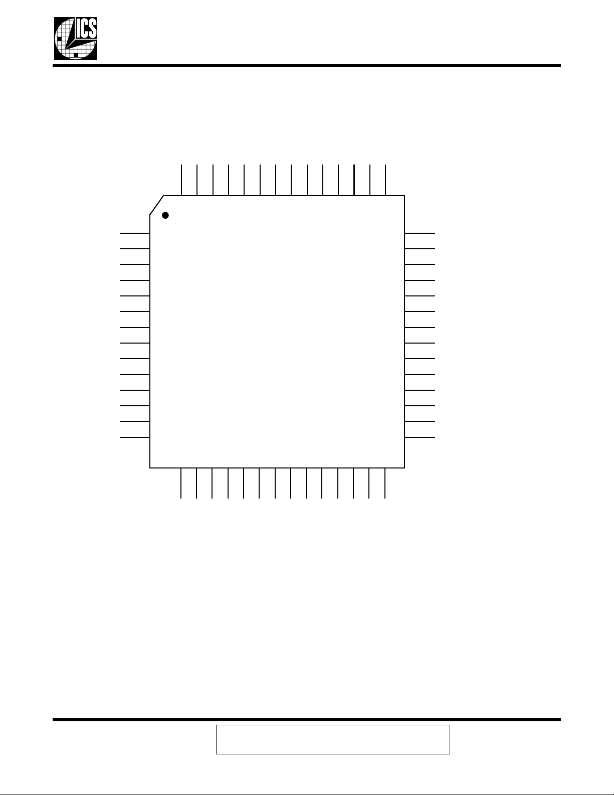
ICS1893CF Data Sheet Rev. F - Release
Chapter 8 Pin Diagram, Listings, and Descriptions
8.3 ICS1893CK Pin Diagram with MDIX Pinout (56L, 8x8 MLF2)
P4RD
VDD
P3TD
VSS
P2LI
P1CL
VSS
P0AC
VDD
REF_IN
REF_OUT
VDD
CRS
COL
56
55
54
53
52
51
50
49
48
47
46
45
44
43
10/100
AMDIX_EN
VSS
TP_AP
TP_AN
VDD
VDD
TP_BN
TP_BP
VSS
VDD
10TCSR
100TCSR
VSS
1
2
3
4
5
6
7
8
9
10
11
12
13
14
16
15
VSS
VDD
ICS1893CK
8x8 56L MLF2
21
20
19
18
17
VSS
VSS
VSS
VSS
RESET_N
26
25
24
23
22
MDIO
VSS
VSS
VDD
VSS
27
MDC
42
41
40
39
38
37
36
35
34
33
32
31
30
29
28
RXD3
TXD3
TXD2
TXD1
TXD0
TXEN
TXCLK
VSS
RXER
RXCLK
VDD
RXDV
RXD0
RXD1
RXD2
ICS1893CF, Rev. F, 03/01/07 Mar. 2007
Copyright © 2007, Integrated Device Technology, Inc.
All rights reserved.
95
Page 96

8.3.1 ICS1893CK Pin Descriptions
The ICS1893CK Pin Signal Descriptions are identical in function to the ICS1893CF except for the Pin
Numbers. See section 8.1 for descriptions.
Table 8-9. ICS1893CK MAC Interface Pins
Signal Name Pin No. Description
MDIO 26 Management Data Input/Output
MDC 27 Management Data Clock
RXD3 28 Receive Data 3
RXD2 29 Receive Data 2
RXD1 30 Receive Data 1
RXD0 31 Receive Data 0
RXDV 32 Receive Data Valid
RXCLK 34 Receive Clock
RXER 35 Receive Error
TXCLK 37 Transmit Clock
TXEN 38 Transmit Enable
Chapter 8 Pin Diagram, Listings, and DescriptionsICS1893CF Data Sheet - Release
TXD0 39 Transmit Data 0
TXD1 40 Transmit Data 1
TXD2 41 Transmit Data 2
TXD3 42 Transmit Data 3
COL 43 Collision Detect
CRS 44 Carrier Sense
Table 8-10. ICS1893CK Multifunction Pins: PHY Address and LED Pins
Signal Name Pin No. Signals Description
P4RD 56 PHYAD[4] / Receive LED
P3TD 54 PHYAD[3] / Transmit LED
P2LI 52 PHYAD[2] / Link LED
P1CL 51 PHYAD[1] / Collision LED
P0AC 49 PHYAD[0] / Activity LED
Table 8-11. ICS1893CK Configuration Pins
Signal Name Pin No. Signals Description
10/100 1 Output Speed indication, High=100baseTX
AMDIX_EN 2 Auto-MDIX Enable (built-in internal 50K Ohm pull-up)
10TCSR 12 10M Transmit Amplitude Current Set Resistor
100TCSR 13 100M Transmit Amplitude Current Set Resistor
ICS1893CF, Rev. F, 03/01/07 Mar. 2007
Copyright © 2007, Integrated Device Technology, Inc.
All rights reserved.
96
Page 97

ICS1893CF Data Sheet Rev. F - Release
Table 8-11. ICS1893CK Configuration Pins
Signal Name Pin No. Signals Description
REF_IN 47 Frequency Ref Input: 25MHz Clock or Crystal
REF_OUT 46 Frequency Ref Output for Crystal
RESETn 17 System Reset (active low)
8.3.2 Transformer Interface Pins
Transformer connections on the ICS1893CK signals TP_AP, TP_AN, TP_BP and TP_BN are shown in
Table 8-12. The previous TP_CT pin used on the ICS1893CF is not used with the ICS1893CK. The typical
Twisted Pair Transformers connections are shown in Chapter 5. The transformer must be 1:1 ratio and
symetrical for 10/100 MDI/MDIX applications since the transmit twisted pair and receive twisted pair are
interchangeable. ICS1893 PHYs do not have power connections to the Transformer. All transformer power
is supplied by the ICS1893CK.
Note the twisted pairs are polarity sensitive and must connect to the RJ45 with the same polarity as shown
in the figure. Pay particular attention to polarity of the the “B” pair being reversed in pad sequence.
Table 8-12. ICS1893CK Transformer Interface Pins
Signal Name Pin No. Signals Description
TP_AP 4 Twisted Pair A Positive
Chapter 8 Pin Diagram, Listings, and Descriptions
TP_AN 5 Twisted Pair A Negative
TP_BP 9 Twisted Pair B Positive
TP_BN 8 Twisted Pair B Negative
ICS1893CF, Rev. F, 03/01/07 Mar. 2007
Copyright © 2007, Integrated Device Technology, Inc.
All rights reserved.
97
Page 98

8.3.3 Ground and Power Pins
Table 8-13. ICS1893CK Ground and Power Pins
Signal Name Pin No. Signals Description
VDD 6 Power 3.3V
VDD 7 Power 3.3V
VDD 11 Power 3.3V
VDD 15 Power 3.3V
VDD 23 Power 3.3V
VDD 33 Power 3.3V
VDD 45 Power 3.3V
VDD 48 Power 3.3V
VDD 55 Power 3.3V
VSS 3 Ground
VSS 10 Ground
VSS 14 Ground
VSS 16 Ground
Chapter 8 Pin Diagram, Listings, and DescriptionsICS1893CF Data Sheet - Release
VSS 18 Ground
VSS 19 Ground
VSS 20 Ground
VSS 21 Ground
VSS 22 Ground
VSS 24 Ground
VSS 25 Ground
VSS 36 Ground
VSS 50 Ground
VSS 53 Ground
ICS1893CF, Rev. F, 03/01/07 Mar. 2007
Copyright © 2007, Integrated Device Technology, Inc.
All rights reserved.
98
Page 99

ICS1893CF Data Sheet Rev. F - Release
Chapter 9 DC and AC Operating Conditions
Chapter 9 DC and AC Operating Conditions
9.1 Absolute Maximum Ratings
Table 9-1 lists absolute maximum ratings. Stresses above these ratings can permanently damage the
ICS1893CF. These ratings, which are standard values for IDT commercially rated parts, are stress ratings
only. Functional operation of the ICS1893CF at these or any other conditions above those indicated in the
operational sections of the specifications is not implied. Exposure to absolute maximum rating conditions
for extended periods can affect product reliability. Electrical parameters are guaranteed only over the range
of the recommended operating temperature.
Table 9-1. Absolute Maximum Ratings for ICS1893CF
Item Rating
VDD (measured to VSS) -0.3 V to 3.6V
Digital Inputs / Outputs -0.3 V to VDD +0.3 V
Storage Temperature -55° C to +150° C
Junction Temperature 125° C
Soldering Temperature 260° C
Power Dissipation See Section 9.4.1, “DC Operating Characteristics for Supply Current”
9.2 Recommended Operating Conditions
Table 9-2. Recommended Operating Conditions for ICS1893CF
Parameter Symbols Min. Max. Units
Ambient Operating Temperature - Commercial T
Ambient Operating Temperature - Industrial T
Power Supply Voltage (measured to VSS) VDD +3.14 +3.47 V
A
A
0+70°C
-40 +85 °C
ICS1893CF, Rev. F, 03/01/07 Mar. 2007
Copyright © 2007, Integrated Device Technology, Inc.
All rights reserved.
99
Page 100

9.3 Recommended Component Values *
e
.
Table 9-3. Recommended Component Values for ICS1893CF
Parameter Minimum Typical Maximum Tolerance Units
Oscillator Frequency – 25 – ± 50 ppm † MHz
10TCSR Resistor Value – 2.43k – 1% Ω
100TCSR Resistor Value – See Figure 9-1 –1%Ω
LED Resistor Value 510 1k 10k – Ω
† There are two IEEE Std. 802.3 requirements that define the tolerance for the frequency of the oscillator.
• Clause 22.2.2.1 requires the MII TX_CLK to have an accuracy of ± 100 ppm.
• Clause 24.2.3.4 is more stringent. It requires the code-bit timer to have an accuracy of 0.005% (that is, ±50 ppm).
Figure 9-1. ICS1893CF 10TCSR and 100TCSR
Typical Board Layouts
10TCSR and 100TCSR Bias Resistors
Chapter 9 DC and AC Operating ConditionsICS1893CF Data Sheet - Release
ICS1893CF
VDD 10TCSR 100TCSR
18 19 20
18.2KΩ 1%
VDD
10TCSR
2.43KΩ 1%
Note:
1. The bias resistor networks set the 10baseT and 100baseTX output amplitude levels.
2. Amplitude is directly related to current sourced out of the 10TCSR and 100TCSR pins.
3. Resistor values shown above are typical. User should check amplitudes and adjust for transformer effects
4. The VDD connection to the 18.2K resistor can connect to any VDD. The 18.2K resistor provides negativ
feedback to compensate for VDD changes. Lowering the 18.2K value will lower the 100baseT amplitude
100TCSR
1.82KΩ 1%
* For backward compatibillity, refer to the “1893C Alternate Schematic” application note.
ICS1893CF, Rev. F, 03/01/07 Mar. 2007
Copyright © 2007, Integrated Device Technology, Inc.
All rights reserved.
100
 Loading...